SOT89 PNP SILICON POWER
(SWITCHING) TRANSISTOR
ISSSUE 1 - DECEMBER 1998
FEATURES
*
2W POWER DISSIPATION
*
6A Peak Pulse Current
*
Excellent H
FE
Characteristics up to 6Amps
*
Extremely Low Saturation Voltage E.g. 16mv Typ.
*
Extremely Low Equivalent On-resistance;
R
CE(sat)
96m
at 2.5A
Partmarking Detail -
718
ABSOLUTE MAXIMUM RATINGS.
PARAMETER
SYMBOL
VALUE
UNIT
Collector-Base Voltage
V
CBO
-20
V
Collector-Emitter Voltage
V
CEO
-20
V
Emitter-Base Voltage
V
EBO
-5
V
Peak Pulse Current **
I
CM
-6
A
Continuous Collector Current
I
C
-2.5
A
Base Current
I
B
-500
mA
Power Dissipation at T
amb
=25∞C
P
tot
1
2
W
W
Operating and Storage Temperature Range
T
j
:T
stg
-55 to +150
∞C
recommended P
tot
calculated using FR4 measuring 15x15x0.6mm
Maximum power dissipation is calculated assuming that the device is mounted on FR4
substrate measuring 40x40x0.6mm and using comparable measurement methods adopted by
other suppliers.
**Measured under pulsed conditions. Pulse width=300
µ
s. Duty cycle
2%
Spice parameter data is available upon request for these devices
Refer to the handling instructions for soldering surface mount components.
C
B
C
E
FCX718

ELECTRICAL CHARACTERISTICS (at T
amb
= 25∞C unless otherwise stated).
PARAMETER
SYMBOL
MIN.
TYP.
MAX.
UNIT
CONDITIONS.
Collector-Base
Breakdown Voltage
V
(BR)CBO
-20
-65
V
I
C
=-100
µ
A
Collector-Emitter
Breakdown Voltage
V
(BR)CEO
-20
-55
V
I
C
=-10mA*
Emitter-Base
Breakdown Voltage
V
(BR)EBO
-5
-8.8
V
I
E
=-100
µ
A
Collector Cut-Off
Current
I
CBO
-100
nA
V
CB
=-15V
Emitter Cut-Off Current
I
EBO
-100
nA
V
EB
=-4V
Collector Emitter
Cut-Off Current
I
CES
-100
nA
V
CES
=-15V
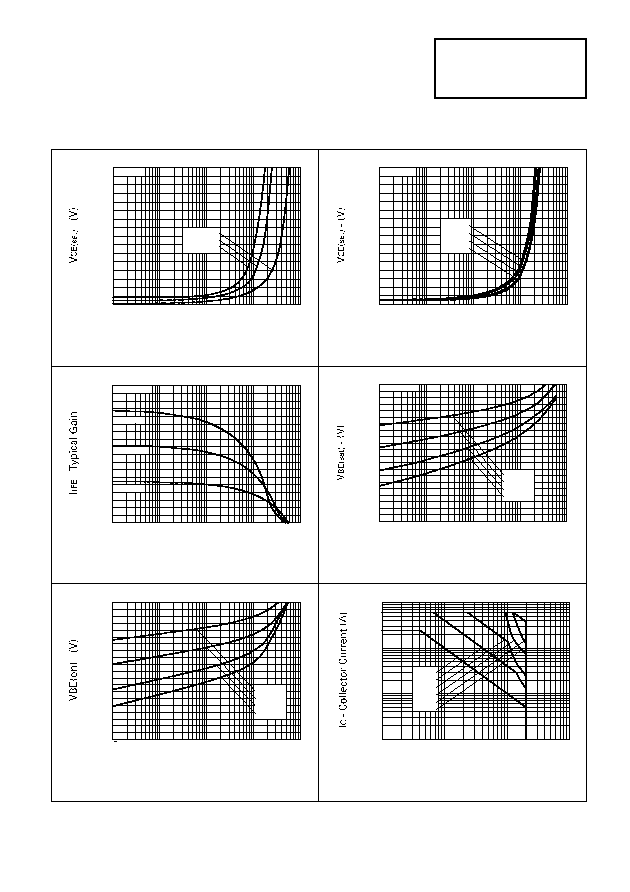
Collector-Emitter
Saturation Voltage
V
CE(sat)
-16
-130
-145
-40
-200
-220
-300
mV
mV
mV
mV
I
C
=-0.1A, I
B
=-10mA*
I
C
=-1A, I
B
=-20mA*
I
C
=-1.5A, I
B
=-50mA*
I
C
=-2.5A, I
B
=-200mA*
Base-Emitter
Saturation Voltage
V
BE(sat)
-0.98
-1.1
V
I
C
=-2.5A, I
B
=-200mA*
Base-Emitter Turn-On
Voltage
V
BE(on)
-0.85
-0.95
V
I
C
=-2.5A, V
CE
=-2V*
Static Forward Current
Transfer
Ratio
h
FE
300
300
150
35
15
475
450
230
70
30
I
C
=-10mA, V
CE
=-2V*
I
C
=-0.1A, V
CE
=-2V*
I
C
=-2A, V
CE
=-2V*
I
C
=-4A, V
CE
=-2V*
I
C
=-6A, V
CE
=-2V*
Transition
Frequency
f
T
150
180
MHz
I
C
=-50mA, V
CE
=-10V
f=100MHz
Output Capacitance
C
obo
21
30
pF
V
CB
=-10V, f=1MHz
Turn-On Time
t
(on)
40
ns
V
CC
=-15V, I
C
=-0.75A
I
B1
=I
B2
=15mA
Turn-Off Time
t
(off)
670
ns
*Measured under pulsed conditions. Pulse width=300
µ
s. Duty cycle
2%
FCX718