 | –≠–ª–µ–∫—Ç—Ä–æ–Ω–Ω—ã–π –∫–æ–º–ø–æ–Ω–µ–Ω—Ç: FXT618 | –°–∫–∞—á–∞—Ç—å:  PDF PDF  ZIP ZIP |

NPN SILICON PLANAR MEDIUM POWER
HIGH GAIN TRANSISTOR
ISSUE 2 JULY 1995
FEATURES
* 10A Peak pulse current
* Excellent h
FE
characteristics up to10A (pulsed)
* Extremely low saturation voltage e.g. 7mV typ.
* I
C
cont 3.5A
APPLICATIONS
* Power MOSFET gate driver in conjunction with
complementary ZTX718
ABSOLUTE MAXIMUM RATINGS.
PARAMETER
SYMBOL
VALUE
UNIT
Collector-Base Voltage
V
CBO
20
V
Collector-Emitter Voltage
V
CEO
20
V
Emitter-Base Voltage
V
EBO
5
V
Peak Pulse Current
I
CM
10
A
Continuous Collector Current
I
C
3.5
A
Base Current
I
B
500
mA
Practical Power Dissipation*
P
totp
1.5
W
Power Dissipation
P
tot
1
W
Operating and Storage Temperature Range
T
j
:T
stg
-55 to +200
∞C
* Device mounted on P.C.B. with copper equal to 1 sq. Inch minimum.
ZTX618
ZTX618
C
B
E
E-Line
TO92 Compatible
D=1(D.C.)
D=0.2
D=0.1
D=0.05
D=0.5
Single Pulse
D=t1
tP
t1
tP
Transient Thermal Resistance
Pulse Width
0.1ms
20
60
100
140
180
1ms
10ms
100ms
10s
100s
1s
160
120
80
40
0
Derating curve
T -Temperature (∞ C)
M
ax
P
ow
er
Di
ssi
p
at
i
on
-
(W
a
t
t
s)
-40
0.50
0.25
1.0
0.75
0
40
80
120
200
160
Am
bie
nt tem
per
atur
e
THERMAL CHARACTERISTICS
PARAMETER
SYMBOL
MAX.
UNIT
Thermal Resistance:
Junction to Ambient
1
Junction to Ambient
2
R
th(j-amb)1
R
th(j-amb)2
175
116
∞C/W
∞C/W
Device mounted on P.C.B. with copper equal to 1 sq. Inch minimum.
Zetex plc.
Fields New Road, Chadderton, Oldham, OL9-8NP, United Kingdom.
Telephone: (44)161 622 4422 (Sales), (44)161 622 4444 (General Enquiries)
Fax: (44)161 622 4420
Zetex GmbH
Zetex Inc.
Zetex (Asia) Ltd.
These are supported by
Streitfeldstraþe 19
47 Mall Drive, Unit 4
3510 Metroplaza, Tower 2
agents and distributors in
D-81673 M¸nchen
Commack NY 11725
Hing Fong Road,
major countries world-wide
Germany
USA
Kwai Fong, Hong Kong
©
Zetex plc 1997
Telefon: (49) 89 45 49 49 0
Telephone: (516) 543-7100
Telephone:(852) 26100 611
Internet:
Fax: (49) 89 45 49 49 49
Fax: (516) 864-7630
Fax: (852) 24250 494
http://www.zetex.com
This publication is issued to provide outline information only which (unless agreed by the Company in writing) may not be used, applied
or reproduced for any purpose or form part of any order or contract or be regarded as a representation relating to the products or
services concerned. The Company reserves the right to alter without notice the specification, design, price or conditions of supply of any
product or service.

0.2
0
0.3
0
0.1
0.4
0.2
0.3
-55∞C
100∞C
25∞C
I
+
/I
*
=50
I
+
/I
*
=10
I
+
/I
*
=50
I
+
/I
*
=100
25∞C
25∞C
100∞C
-55∞C
25∞C
100∞C
-55∞C
I
+
/I
*
=50
V
+-
=2V
25∞C
100∞C
-55∞C
V
+-
=2V
1.0
0.8
0.4
0.6
0.2
0
1.2
1
10
0.01
0.1
100V
10V
1V
0.1V
0
0.2
450
225
0.4
0.1
1mA
100mA
10mA
1A
10A
10A
1A
100mA
10mA
1mA
10A
1A
10mA
100mA
1mA
1mA
100mA
10mA
1A
10A
1mA
100mA
10mA
1A
10A
0.4
0.8
0.6
0
1.0
100
µ
s
10ms
1s
DC
100ms
1ms
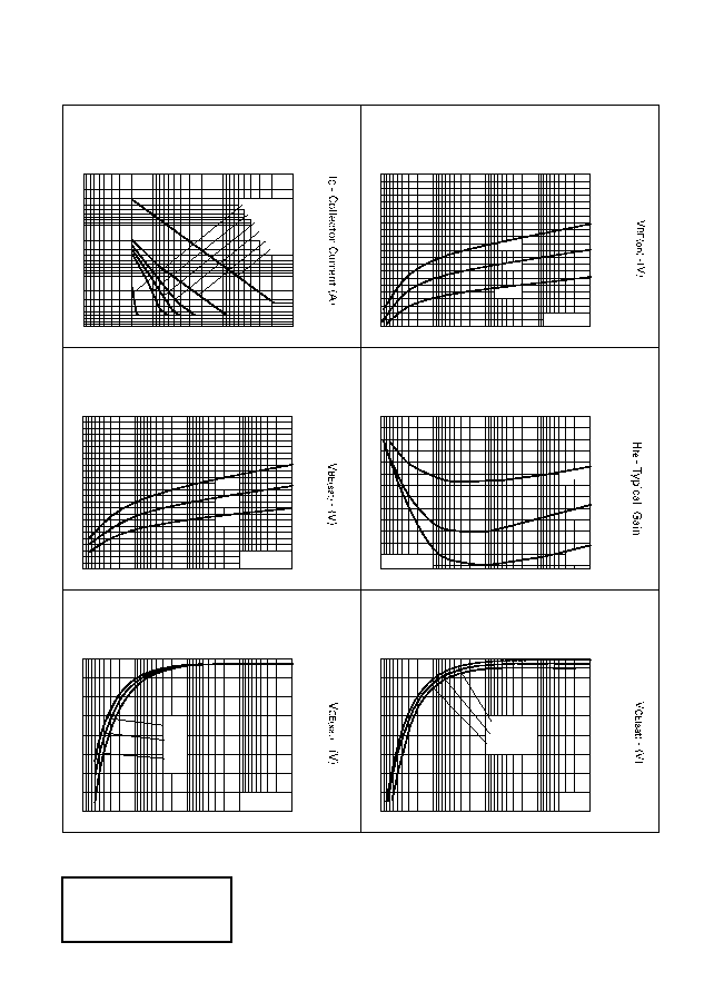
I
C
-Collector Current
I
C
-Collector Current
I
C
-Collector Current
I
C
-Collector Current
I
C
-Collector Current
h
FE
v I
C
V
BE(sat)
v Ic
V
BE(on)
v I
C
V
CE(sat)
v I
C
V
CE(sat)
v I
C
V
CE
- Collector Voltage
Safe Operating Area
Single Pulse Test Tamb=25C
TYPICAL CHARACTERISTICS
ELECTRICAL CHARACTERISTICS (at T
amb
= 25∞C unless otherwise stated).
PARAMETER
SYMBOL
MIN.
TYP.
MAX. UNIT CONDITIONS.
Collector-Base
Breakdown Voltage
V
(BR)CBO
20
100
V
I
C
=100
µ
A
Collector-Emitter
Breakdown Voltage
V
(BR)CEO
20
27
V
I
C
=10mA*
Emitter-Base
Breakdown Voltage
V
(BR)EBO
5
8.3
V
I
E
=100
µ
A
Collector Cut-Off
Current
I
CBO
100
nA
V
CB
=16V
Emitter Cut-Off
Current
I
EBO
100
nA
V
EB
=4V
Collector Emitter
Cut-Off Current
I
CES
100
nA
V
CES
=16V
Collector-Emitter
Saturation Voltage
V
CE(sat)
7
80
210
15
150
255
mV
mV
mV
I
C
=0.1A, I
B
=10mA*
I
C
=1A, I
B
=10mA*
I
C
=3.5A, I
B
=50mA*
Base-Emitter
Saturation Voltage
V
BE(sat)
0.93
1.05
V
I
C
=3.5A, I
B
=50mA*
Base-Emitter
Turn-On Voltage
V
BE(on)
0.86
1.0
V
I
C
=3.5A, V
CE
=2V*
Static Forward
Current Transfer
Ratio
h
FE
200
300
170
40
400
450
300
85
I
C
=10mA, V
CE
=2V*
I
C
=200mA, V
CE
=2V*
I
C
=3A, V
CE
=2V*
I
C
=10A, V
CE
=2V*
Transition
Frequency
f
T
100
140
MHz
I
C
=50mA, V
CE
=10V
f=100MHz
Output Capacitance
C
obo
23
30
pF
V
CB
=10V, f=1MHz
Turn-On Time
t
(on)
170
ns
V
CC
=10V, I
C
=1A
I
B1
=-I
B2
=10mA
Turn-Off Time
t
(off)
400
ns
*Measured under pulsed conditions. Pulse width=300
µ
s. Duty cycle
2%
ZTX618
ZTX618
0.2
0
0.3
0
0.1
0.4
0.2
0.3
-55∞C
100∞C
25∞C
I
+
/I
*
=50
I
+
/I
*
=10
I
+
/I
*
=50
I
+
/I
*
=100
25∞C
25∞C
100∞C
-55∞C
25∞C
100∞C
-55∞C
I
+
/I
*
=50
V
+-
=2V
25∞C
100∞C
-55∞C
V
+-
=2V
1.0
0.8
0.4
0.6
0.2
0
1.2
1
10
0.01
0.1
100V
10V
1V
0.1V
0
0.2
450
225
0.4
0.1
1mA
100mA
10mA
1A
10A
10A
1A
100mA
10mA
1mA
10A
1A
10mA
100mA
1mA
1mA
100mA
10mA
1A
10A
1mA
100mA
10mA
1A
10A
0.4
0.8
0.6
0
1.0
100
µ
s
10ms
1s
DC
100ms
1ms
I
C
-Collector Current
I
C
-Collector Current
I
C
-Collector Current
I
C
-Collector Current
I
C
-Collector Current
h
FE
v I
C
V
BE(sat)
v Ic
V
BE(on)
v I
C
V
CE(sat)
v I
C
V
CE(sat)
v I
C
V
CE
- Collector Voltage
Safe Operating Area
Single Pulse Test Tamb=25C
TYPICAL CHARACTERISTICS
ELECTRICAL CHARACTERISTICS (at T
amb
= 25∞C unless otherwise stated).
PARAMETER
SYMBOL
MIN.
TYP.
MAX. UNIT CONDITIONS.
Collector-Base
Breakdown Voltage
V
(BR)CBO
20
100
V
I
C
=100
µ
A
Collector-Emitter
Breakdown Voltage
V
(BR)CEO
20
27
V
I
C
=10mA*
Emitter-Base
Breakdown Voltage
V
(BR)EBO
5
8.3
V
I
E
=100
µ
A
Collector Cut-Off
Current
I
CBO
100
nA
V
CB
=16V
Emitter Cut-Off
Current
I
EBO
100
nA
V
EB
=4V
Collector Emitter
Cut-Off Current
I
CES
100
nA
V
CES
=16V
Collector-Emitter
Saturation Voltage
V
CE(sat)
7
80
210
15
150
255
mV
mV
mV
I
C
=0.1A, I
B
=10mA*
I
C
=1A, I
B
=10mA*
I
C
=3.5A, I
B
=50mA*
Base-Emitter
Saturation Voltage
V
BE(sat)
0.93
1.05
V
I
C
=3.5A, I
B
=50mA*
Base-Emitter
Turn-On Voltage
V
BE(on)
0.86
1.0
V
I
C
=3.5A, V
CE
=2V*
Static Forward
Current Transfer
Ratio
h
FE
200
300
170
40
400
450
300
85
I
C
=10mA, V
CE
=2V*
I
C
=200mA, V
CE
=2V*
I
C
=3A, V
CE
=2V*
I
C
=10A, V
CE
=2V*
Transition
Frequency
f
T
100
140
MHz
I
C
=50mA, V
CE
=10V
f=100MHz
Output Capacitance
C
obo
23
30
pF
V
CB
=10V, f=1MHz
Turn-On Time
t
(on)
170
ns
V
CC
=10V, I
C
=1A
I
B1
=-I
B2
=10mA
Turn-Off Time
t
(off)
400
ns
*Measured under pulsed conditions. Pulse width=300
µ
s. Duty cycle
2%
ZTX618
ZTX618

NPN SILICON PLANAR MEDIUM POWER
HIGH GAIN TRANSISTOR
ISSUE 2 JULY 1995
FEATURES
* 10A Peak pulse current
* Excellent h
FE
characteristics up to10A (pulsed)
* Extremely low saturation voltage e.g. 7mV typ.
* I
C
cont 3.5A
APPLICATIONS
* Power MOSFET gate driver in conjunction with
complementary ZTX718
ABSOLUTE MAXIMUM RATINGS.
PARAMETER
SYMBOL
VALUE
UNIT
Collector-Base Voltage
V
CBO
20
V
Collector-Emitter Voltage
V
CEO
20
V
Emitter-Base Voltage
V
EBO
5
V
Peak Pulse Current
I
CM
10
A
Continuous Collector Current
I
C
3.5
A
Base Current
I
B
500
mA
Practical Power Dissipation*
P
totp
1.5
W
Power Dissipation
P
tot
1
W
Operating and Storage Temperature Range
T
j
:T
stg
-55 to +200
∞C
* Device mounted on P.C.B. with copper equal to 1 sq. Inch minimum.
ZTX618
ZTX618
C
B
E
E-Line
TO92 Compatible
D=1(D.C.)
D=0.2
D=0.1
D=0.05
D=0.5
Single Pulse
D=t1
tP
t1
tP
Transient Thermal Resistance
Pulse Width
0.1ms
20
60
100
140
180
1ms
10ms
100ms
10s
100s
1s
160
120
80
40
0
Derating curve
T -Temperature (∞ C)
M
ax
P
ow
er
Di
ssi
p
at
i
on
-
(W
a
t
t
s)
-40
0.50
0.25
1.0
0.75
0
40
80
120
200
160
Am
bie
nt tem
per
atur
e
THERMAL CHARACTERISTICS
PARAMETER
SYMBOL
MAX.
UNIT
Thermal Resistance:
Junction to Ambient
1
Junction to Ambient
2
R
th(j-amb)1
R
th(j-amb)2
175
116
∞C/W
∞C/W
Device mounted on P.C.B. with copper equal to 1 sq. Inch minimum.
Zetex plc.
Fields New Road, Chadderton, Oldham, OL9-8NP, United Kingdom.
Telephone: (44)161 622 4422 (Sales), (44)161 622 4444 (General Enquiries)
Fax: (44)161 622 4420
Zetex GmbH
Zetex Inc.
Zetex (Asia) Ltd.
These are supported by
Streitfeldstraþe 19
47 Mall Drive, Unit 4
3510 Metroplaza, Tower 2
agents and distributors in
D-81673 M¸nchen
Commack NY 11725
Hing Fong Road,
major countries world-wide
Germany
USA
Kwai Fong, Hong Kong
©
Zetex plc 1997
Telefon: (49) 89 45 49 49 0
Telephone: (516) 543-7100
Telephone:(852) 26100 611
Internet:
Fax: (49) 89 45 49 49 49
Fax: (516) 864-7630
Fax: (852) 24250 494
http://www.zetex.com
This publication is issued to provide outline information only which (unless agreed by the Company in writing) may not be used, applied
or reproduced for any purpose or form part of any order or contract or be regarded as a representation relating to the products or
services concerned. The Company reserves the right to alter without notice the specification, design, price or conditions of supply of any
product or service.