 | –≠–ª–µ–∫—Ç—Ä–æ–Ω–Ω—ã–π –∫–æ–º–ø–æ–Ω–µ–Ω—Ç: ZAMP001 | –°–∫–∞—á–∞—Ç—å:  PDF PDF  ZIP ZIP |

S E M I C O N D U C T O R S
DESCRIPTION
The ZAMP001 is an low current low noise amplifier
designed for L band and IF applications. Although the
ZAMP001 has been designed primarily for DBS
applications the ZAMP001 is capable of extending to
frequencies of 2.5GHz so it has a good fit with various
applications. An additional benefit of the ZAMP001 is
it's rising gain characteristic, this has been designed to
counteract the gain losses found at the higher
frequencies.
The ZAMP001 has been optimized for
input and output impedances of 50 ohms.
The
ZAMP001 complements the buffer amplifiers in the
ZAMP series to give a low current high performance
optimum solution. Packaged in a small SC70-6 with
the minimum number of external bias components
required it is the ideal solution for space and current
limited applications.
FEATURES
∑
L and IF frequency band
∑
Low noise 5dB @ 1GHz
∑
Low current consumption 12mA typical
∑
Gain 18dB typical
∑
Rising gain
∑
IP3 8dBm @ 1Ghz
∑
4.5 to 5.5V Supply Voltage
∑
Unconditionally stable
∑
SC70-6 SMD package
APPLICATIONS
∑
Satellite LNB receivers
∑
Set-top boxes
∑
TV tuners
∑
SMR (Special Mobile Radio)
∑
RLAN/WLAN
∑
General purpose
ZAMP001
ISSUE 2 - MARCH 2003
1
800-2500MHz MMIC WIDEBAND AMPLIFIER
LNA, 18dB Gain, Low Current
DEVICE
REEL
SIZE
(inches)
QUANTITY
PER REEL
DEVICE
MARKING
ZAMP001H6TA
7
3000 units
ZP01
ZAMP001H6TC
13"
10000 units
ZP01
ORDERING INFORMATION
Top View
GND
GND
INPUT
1
2
3
OUTPUT
GND
V
CC
6
5
4
CONNECTION DIAGRAM
SC70-6
ABSOLUTE MAXIMUM RATINGS
Supply Voltage
7V
Supply Current
30mA
Operating Temperature
-40 to 85∞C
Storage Temperature
-50 to 125∞C
ZAMP001
S E M I C O N D U C T O R S
ISSUE 2 - MARCH 2003
2
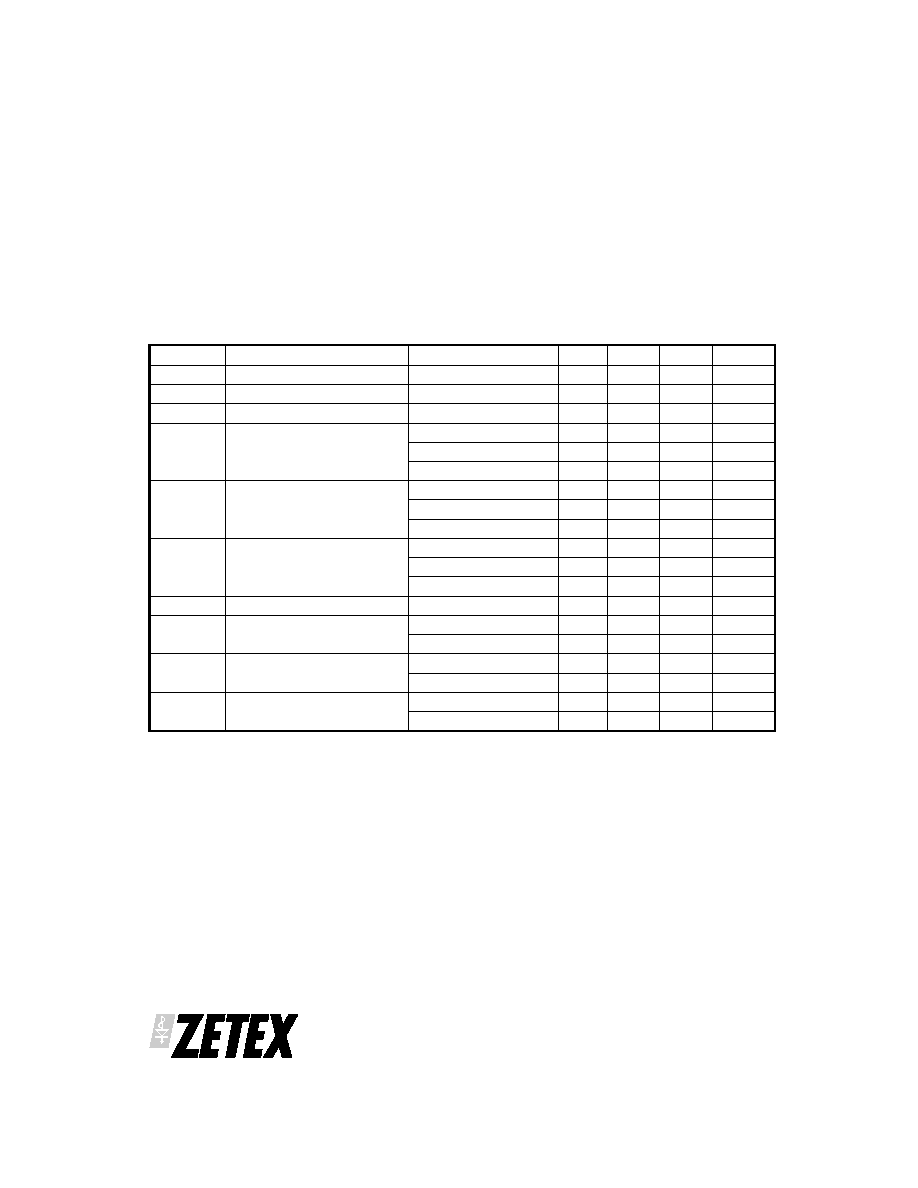
SYMBOL
PARAMETER
CONDITIONS
MIN
TYP.
MAX
UNITS
F
O
Operating Frequency
800
2500
MHz
V
CC
Supply Voltage
4.5
5
5.5
V
I
CC
Supply Current
12.2
14.4
mA
Gp
Power Gain
F = 950 MHz
17
18
dB
F = 1550 MHz
18.2
dB
F = 2150 MHz
18.5
20
dB
NF
Noise Figure
F = 950 MHz
5
dB
F = 1550 MHz
dB
F = 2150 MHz
6.5
dB
IP3
3rd Order Intercept Point
F = 950 MHz
5
8
dBm
F = 1550 MHz
7
dBm
F = 2150 MHz
8
dBm
P1dB
1dB Gain Compression
F = 950 to 2150 MHz
-6
-2
dBm
RL
IN
Input Return Loss
F = 950 MHz
9
dB
F = 2150 MHz
10
dB
RL
OUT
Output Return Loss
F = 950 MHz
17
dB
F = 2150 MHz
12
dB
Risol
Reverse Isolation
F = 950 MHz
38
dB
F = 2150 MHz
48
dB
ELECTRICAL CHARACTERISTICS
Test Conditions (unless otherwise stated): VCC = 5V, Tamb = 25∞C, Zo = 50 .
ZAMP001
S E M I C O N D U C T O R S
ISSUE 2 - MARCH 2003
3
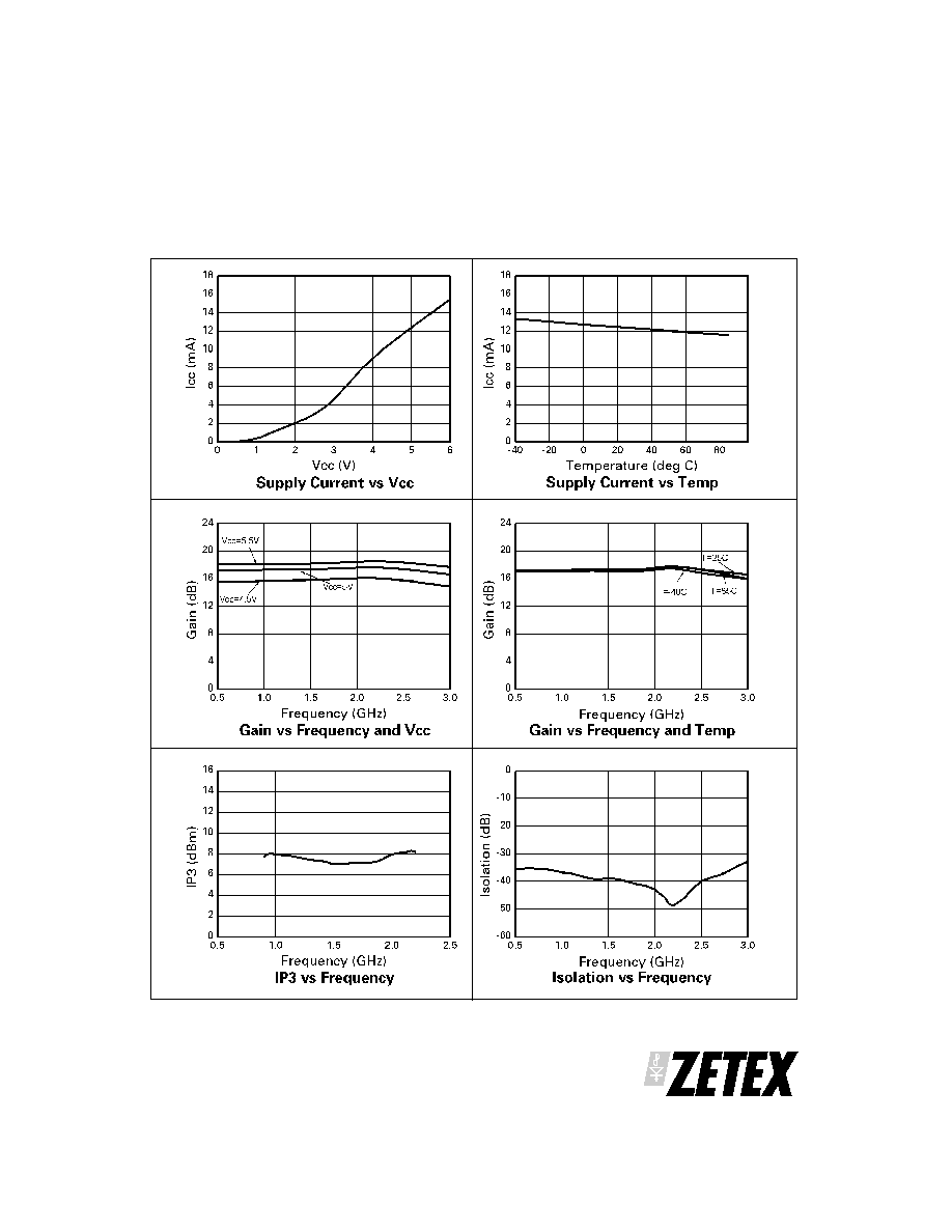
TYPICAL CHARACTERISTICS
Test Conditions (unless otherwise stated): V
CC
= 5V, T
amb
= 25∞C, Zo = 50 .
ZAMP001
S E M I C O N D U C T O R S
ISSUE 2 - MARCH 2003
4
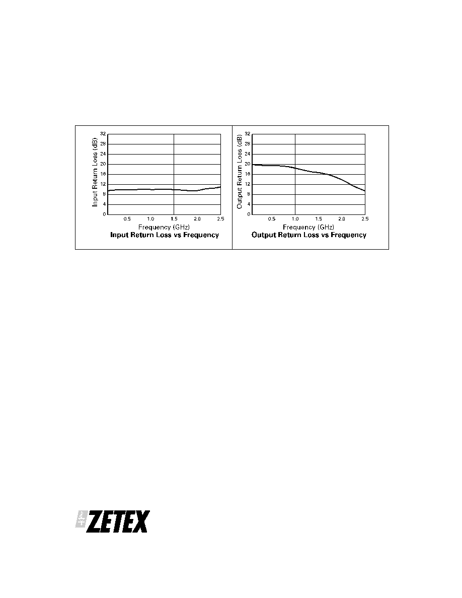
TYPICAL CHARACTERISTICS
ZAMP001
S E M I C O N D U C T O R S
ISSUE 2 - MARCH 2003
5
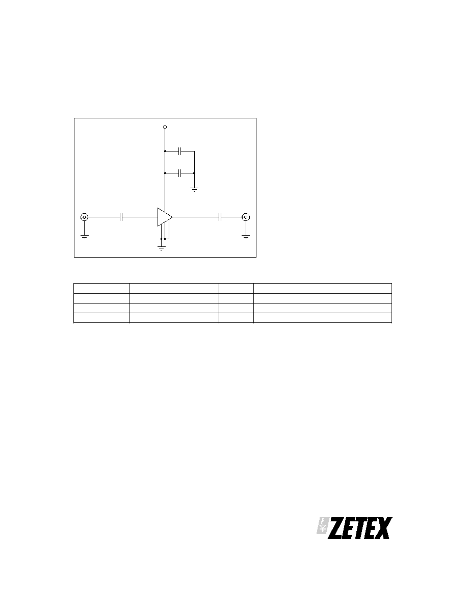
C4
100nF
X7R
C1
100pF
NPO
C2
100pF
NPO
J2
C3
100pF
NPO
3
6
1
5
4
2
IC1
ZAMP001
J1
Vcc
TEST CIRCUIT
TEST CIRCUIT COMPONENTS LIST
Circuit Ref.
Description
Value
Type
C1,C2,C3
Chip ceramic capacitor
100 pF
Murata GRH708 series, size 0805
C4
Chip ceramic capacitor
100 nF
X7R, size 0805
IC1
ZAMP001
Wideband Amplifier, SC70-6
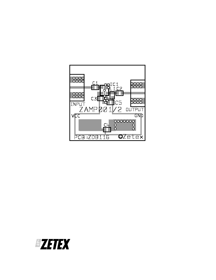
Note: For ZAMP001, L1 and C5 are not fitted.
APPLICATION NOTES
The ZAMP001 is a wideband RFIC amplifier designed
for use primarily in DBS applications. The amplifier is
designed to provide both a 50 Ohm input and output
impedance and thus requires no additional matching
components. The input and output signal connections
each require a DC blocking capacitor (C1 and C2). A
suitable value for these capacitors is around 100pF for
the 950MHz to 2150MHz frequency range. For other
frequency ranges the value of the capacitor should be
such that its reactance at the lowest operating
frequency is small when compared to 50 ohms. Supply
de-coupling is also recommended and should take the
form of a suitable 100pF capacitor, C3, for the 950MHz
to 2150MHz frequency range.
The 100pF capacitor
should be mounted as close to the Vcc pin of the
amplifier as is physically possible. An additional low
frequency de-coupling capacitor, C4, with a value
around 100nF is also advised.
An example layout for a test board for the ZAMP series
can be seen above. This was designed for an FR4 board
1 x 1 inch, 0.016 inch thick with a copper thickness of 35
microns. Edge mounted SMA connectors were used
for the RF signals. The inductor is not required for
ZAMP001.
ZAMP001
S E M I C O N D U C T O R S
ISSUE 2 - MARCH 2003
6
TEST CIRCUIT LAYOUT

Notes
ZAMP001
S E M I C O N D U C T O R S
ISSUE 2 - MARCH 2003
7
Europe
Zetex plc
Fields New Road
Chadderton
Oldham, OL9 8NP
United Kingdom
Telephone (44) 161 622 4444
Fax: (44) 161 622 4446
hq@zetex.com
Zetex GmbH
Streitfeldstraþe 19
D-81673 M¸nchen
Germany
Telefon: (49) 89 45 49 49 0
Fax: (49) 89 45 49 49 49
europe.sales@zetex.com
Americas
Zetex Inc
700 Veterans Memorial Hwy
Hauppauge, NY 11788
USA
Telephone: (1) 631 360 2222
Fax: (1) 631 360 8222
usa.sales@zetex.com
Asia Pacific
Zetex (Asia) Ltd
3701-04 Metroplaza Tower 1
Hing Fong Road
Kwai Fong
Hong Kong
Telephone: (852) 26100 611
Fax: (852) 24250 494
asia.sales@zetex.com
These offices are supported by agents and distributors in major countries world-wide.
This publication is issued to provide outline information only which (unless agreed by the Company in writing) may not be used, applied or reproduced
for any purpose or form part of any order or contract or be regarded as a representation relating to the products or services concerned. The Company
reserves the right to alter without notice the specification, design, price or conditions of supply of any product or service.
For the latest product information, log on to
www.zetex.com
© Zetex plc 2003
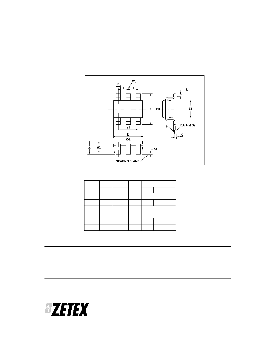
PACKAGE DIMENSIONS SC706
ZAMP001
S E M I C O N D U C T O R S
8
ISSUE 2 - MARCH 2003
DIM
MILLIMETRES
DIM
MILLIMETRES
MIN
MAX
MIN
MAX
A
1.00
E
2.10 BSC
A1
0.10
E1
1.25
1.35
A2
0.70
0.90
e
0.65 BSC
b
0.15
0.30
e1
1.30 BSC
C
0.08
0.25
L
0.26
0.46
D
2.00 BSC
0
8
PACKAGE DIMENSIONS