 | –≠–ª–µ–∫—Ç—Ä–æ–Ω–Ω—ã–π –∫–æ–º–ø–æ–Ω–µ–Ω—Ç: ZDS1009 | –°–∫–∞—á–∞—Ç—å:  PDF PDF  ZIP ZIP |
ISSUE 2 - JANUARY 2000
ZDS1009
SM-8 COMPLEMENTARY CURRENT MIRROR
1
FEATURES
∑
Excellent Temperature Tracking Characteristics
∑
Compact Cost Effective Solution
∑
Simplifies Circuit Implementation
∑
Broad application base from
Single Cell Li-ion High Side Current sense chargers to
Multi-cell Lead-Acid systems
∑
Only 4 Connections required
DESCRIPTION
The ZDS1009 current mirror has been developed
specifically for high side, current sense plus level
translation applications and as such will find a broad
a p p l i c a t i o n s
b a s e
i n c l u d i n g
b a t t e r y
c h a r g e
management, DC motor control and over current
monitoring functions. It is of particular interest for
current sense applications for feedback purposes in fast
battery chargers for Li-Ion cell based systems.
The device functions by sensing the voltage developed
across an external (user defined) high side current
sense resistor, and by an arrangement of current
mirrors refer this sensed voltage, with or without
multiplication, to a low side referenced signal. This
signal can then be used, for example, to close the
control loop to a controller IC, for a DC-DC converter
providing charge to a battery.
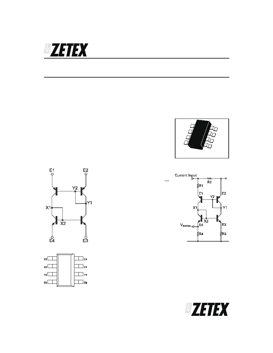
TYPICAL APPLICATION CIRCUIT
V
IR
R
R
sense
2
4
1
=
For balance R3=R4
eg
R2=100m
R1=R3=R4=100
V
sense
sensitivity = 100mV/A
SM-8
(8 LEAD SOT223)
SCHEMATIC DIAGRAM
CONNECTION DIAGRAM
ISSUE 2 - JANUARY 2000
ZDS1009
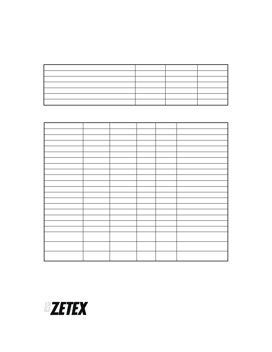
Parameter
Symbol
Min
Max
Unit
Conditions
Breakdown Voltage
BV
Y1-X1
120
V
I
Y1
=100
µ
A
Breakdown Voltage
BV
X1-E1
-30
V
I
X1
=-10mA
Breakdown Voltage
BV
Y1-E3
30
V
I
Y1
=10mA
Breakdown Voltage
BV
E1-Y1
-12
V
I
E1
=-100
µ
A
Breakdown Voltage
BV
E2-Y1
-6
V
I
E2
=-100
µ
A
Breakdown Voltage
BV
E3-X1
12
V
I
E3
=100
µ
A
Breakdown Voltage
BV
E4-X1
6
V
I
E4
=100uA
Leakage
I
Y1
50
nA
V
Y1-X1
=100V
Leakage
I
X1
-10
µ
A
V
X1-E1
=-30V, V
y1
=V
E1
Leakage
I
Y1
10
µ
A
V
Y1-E3
=30V,V
X1
=V
E3
Leakage
I
E1
-100
nA
V
E1-Y1
=-8V
Leakage
I
E2
-100
nA
V
E2-Y1
=-4V
Leakage
I
E3
100
nA
V
E3-X1
=8V
Leakage
I
E4
100
nA
V
E4-X1
=4V
Input Voltage
V
Y1-E2
-1.45
-1.65
V
I
Y1
=-1A
Input Voltage
V
Y1-E3
1.45
1.75
V
I
Y1
=1A,V
X1
=V
Y1
Input Voltage
V
X1-E1
-1.45
-1.75
V
I
X1
=-1A,V
X1
=V
Y1
Input Voltage
V
X1-E4
1.45
1.65
V
I
X1
=1A
Transfer
Characteristic
V
OUT
0.99
1.01
V
See Fig 1.V
CC
=5V
R1=R3=R4=100
, V
IN
=1V
Transfer
Characteristic
V
OUT
1
mV
See Fig 1.V
CC
=5V
R1=R3=R4=100
, V
IN
=5mV
Output Zero-Offset
Voltage
V
OFFSET
4
mV
See Fig 2.V
CC
=5V,R
2
<1
R1=R3=R4=100
ABSOLUTE MAXIMUM RATINGS.
PARAMETER
SYMBOL
VALUE
UNIT
Maximum Operating Voltage
V
y1-x1
120
V
Maximum Voltage (E1-E2,E3-E4)
V
E-E'
10
V
Peak Pulse Current
I
M
4
A
Continuous Current (E1-E4,E2-E3)
I
C
1
A
Total Power Dissipation at T
amb
= 25∞C*
P
tot
2
W
Operating and Storage Temperature Range
T
j
:T
stg
-55 to +150
∞C
* The power which can be dissipated assuming the device is mounted in a typical manner on a PCB with copper
equal to 2 inches square.
ELECTRICAL CHARACTERISTICS (at T
amb
=25∞C)
2
ISSUE 2 - JANUARY 2000
ZDS1009
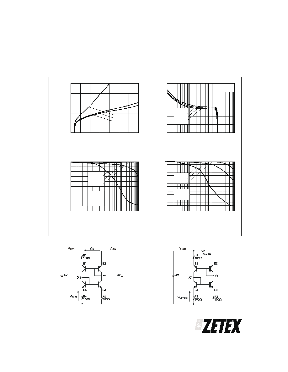
Figure 1
Transfer Characteristic Test Circuit
Figure 2
Output Zero-Offset Voltage Test Circuit
3
Vo
l
t
a
g
e
T
r
a
n
s
f
e
r
10m
Vin - Input Voltage (V)
Frequency (Hz)
Phase Change v Frequency Response
Pha
s
e
C
h
a
nge
(
Degr
ees)
360
240
220
Voltage Transfer v Frequency Response
Frequency (Hz)
100
Vo
l
t
a
g
e
T
r
a
n
s
f
e
r
0.50
V
cc
- Supply Voltage(V)
Voltage Transfer v Supply Voltage
Vo
l
t
a
g
e
T
r
a
n
s
f
e
r
0.95
+25∞C
R = 10
1k
R = 100
R = 1 k
0.7
200
180
5
10
15
20
25
30
35
0
1.00
1.05
1.10
1.15
1.20
100m
1
10
0.8
0.9
1.0
1.1
1.2
1.3
R = 10
R = 100
R = 1 k
0.60
0.70
0.80
0.90
1.00
R = 10k
R = 1k
1k
10k
100k
1M
260
280
300
320
340
10k
100k
1M
Vin = 0.1V
Voltage Transfer v Input Voltage
R = 100
R = 10k
R = 1k
R = 100
Vcc=5V
+25∞C
Vin = 1V
Vcc = 5V
VAC = 0.1V
T = 25∞C
Vin = 1V
Vcc = 5V
VAC = 0.1V
T = 25∞C
TYPICAL CHARACTERISTICS
TEST CIRCUITS

ISSUE 2 - JANUARY 2000
ZDS1009
4
Vo
l
t
a
g
e
-
(
V
)
100µ
0
0.2
0.4
Temperature (∞C)
-55
Vo
l
t
a
g
e
(
V
)
1m
V
ce
(V) - Collector-Emitter Voltage (V)
Curr
ent
T
ransfer
0.95
I
in
- Input Current (A)
Vo
l
t
a
g
e
-
(
V
)
100µA
0.4
+25∞C
Vin
1mA
100µA
Vcutoff
0.1
-60
Vcutoff
0.4
0.6
0.8
1mA
10mA
100mA
1A
0.6
0.8
1.0
1.2
1.4
1m
10m
100mA
1A
0.6
0.8
1.0
1.2
1.4
Vin
Vcutoff
1
10
100
0.96
0.97
0.98
0.99
1.00
1.01
1.02
1.03
1.04
1.05
1
10
1.05
1.04
1.03
1.02
1.01
1.00
0.99
0.98
0.97
0.96
0.95
V
ce
- Collector-Emitter Voltage(V)
Curr
ent
T
ransfer
10mA
100µA
1mA
10mA
Vin
-35
-15
5
25
45
65
85
105
125
Vcutoff
Vin
-40
-20
0
20
40
60
80
100 120
1.0
1.2
1.4
1.6
I
in
- Input Current (A)
+25∞C
1.6
1.4
1.2
1.0
0.8
0.6
0.4
0.2
0
Temperature (∞C)
Iin = 1mA
Iout = 0.95mA
Iin = 1mA
Iout = 0.95mA
Vo
l
t
a
g
e
(
V
)
+25∞C
25 C
Current Transfer v Vce
Input/Cutoff Voltage v I
in
Input/Cutoff Voltage v I
in
Input/Output Voltage v Temperature
Input/Output Voltage v Temperature
Current Transfer v Vce
Iout = 0.95Iin
Iout = 0.95Iin
NPN
NPN
NPN
PNP
PNP
PNP
TYPICAL CHARACTERISTICS
ISSUE 2 - JANUARY 2000
ZDS1009
5
Zetex plc.
Fields New Road, Chadderton, Oldham, OL9 8NP, United Kingdom.
Telephone: (44)161 622 4422 (Sales), (44)161 622 4444 (General Enquiries)
Fax: (44)161 622 4420
Zetex GmbH
Zetex Inc.
Zetex (Asia) Ltd.
These are supported by
Streitfeldstraþe 19
47 Mall Drive, Unit 4
3510 Metroplaza, Tower 2
agents and distributors in
D-81673 M¸nchen
Commack NY 11725
Hing Fong Road,
major countries world-wide
Germany
USA
Kwai Fong, Hong Kong
© Zetex plc 2000
Telefon: (49) 89 45 49 49 0
Telephone: (631) 543-7100
Telephone:(852) 26100 611
Fax: (49) 89 45 49 49 49
Fax: (631) 864-7630
Fax: (852) 24250 494
Internet:http://www.zetex.com
This publication is issued to provide outline information only which (unless agreed by the Company in writing) may not be used, applied or reproduced
for any purpose or form part of any order or contract or be regarded as a representation relating to the products or services concerned. The Company
reserves the right to alter without notice the specification, design, price or conditions of supply of any product or service.
He
E
e1
Lp
45∞
o
c
1
2
3
4
8
7
6
5
e2
A
A1
DIM
Millimetres
Inches
Min
Typ
Max
Min
Typ
Max
A
-
-
1.7
-
-
0.067
A1
0.02
-
0.1
0.0008
-
0.004
b
-
0.7
-
-
0.028
-
c
0.24
-
0.32
0.009
-
0.013
D
6.3
-
6.7
0.248
-
0.264
E
3.3
-
3.7
0.130
-
0.145
e1
-
4.59
-
-
0.180
-
e2
-
1.53
-
-
0.060
-
He
6.7
-
7.3
0.264
-
0.287
Lp
0.9
-
-
0.035
-
-
-
-
15∞
-
-
15∞
-
10∞
-
-
10∞
-
PACKAGE DIMENSIONS
ORDERING INFORMATION
DEVICE
PARTMARKING
ZDS1009
S1009