SM-8 DUAL PNP MEDIUM POWER
TRANSISTORS
ISSUE 1 - AUGUST 1997
PARTMARKING DETAIL ≠ T751
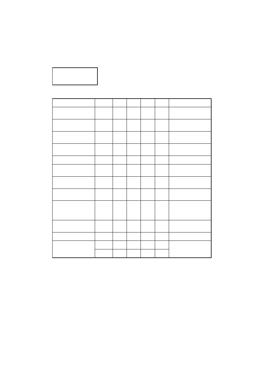
ABSOLUTE MAXIMUM RATINGS.
PARAMETER
SYMBOL
VALUE
UNIT
Collector-Base Voltage
V
CBO
-80
V
Collector-Emitter Voltage
V
CEO
-60
V
Emitter-Base Voltage
V
EBO
-5
V
Peak Pulse Current
I
CM
-6
A
Continuous Collector Current
I
C
-2
A
Operating and Storage Temperature Range
T
j
:T
stg
-55 to +150
∞C
THERMAL CHARACTERISTICS
PARAMETER
SYMBOL
VALUE
UNIT
Total Power Dissipation at T
amb
= 25∞C*
Any single die "on"
Both die "on" equally
P
tot
2.25
2.75
W
W
Derate above 25∞C*
Any single die "on"
Both die "on" equally
18
22
mW/ ∞C
mW/ ∞C
Thermal Resistance - Junction to Ambient*
Any single die "on"
Both die "on" equally
55.6
45.5
∞C/ W
∞C/ W
* The power which can be dissipated assuming the device is mounted in a typical manner
on a PCB with copper equal to 2 inches square.
ZDT751
C
1
C
1
C
2
C
2
B
1
E
1
B
2
E
2
SM-8
(8 LEAD SOT223)
Zetex plc.
Fields New Road, Chadderton, Oldham, OL9-8NP, United Kingdom.
Telephone: (44)161-627 5105 (Sales), (44)161-627 4963 (General Enquiries)
Fax: (44)161-627 5467
Zetex GmbH
Zetex Inc.
Zetex (Asia) Ltd.
These are supported by
Streitfeldstraþe 19
47 Mall Drive, Unit 4
3510 Metroplaza, Tower 2
agents and distributors in
D-81673 M¸nchen
Commack NY 11725
Hing Fong Road,
major countries world-wide
Germany
USA
Kwai Fong, Hong Kong
©
Zetex plc 1997
Telefon: (49) 89 45 49 49 0
Telephone: (516) 543-7100
Telephone:(852) 26100 611
Internet:
Fax: (49) 89 45 49 49 49
Fax: (516) 864-7630
Fax: (852) 24250 494
http://www.zetex.com
This publication is issued to provide outline information only which (unless agreed by the Company in writing) may not be used, applied
or reproduced for any purpose or form part of any order or contract or be regarded as a representation relating to the products or
services concerned. The Company reserves the right to alter without notice the specification, design, price or conditions of supply of any
product or service.
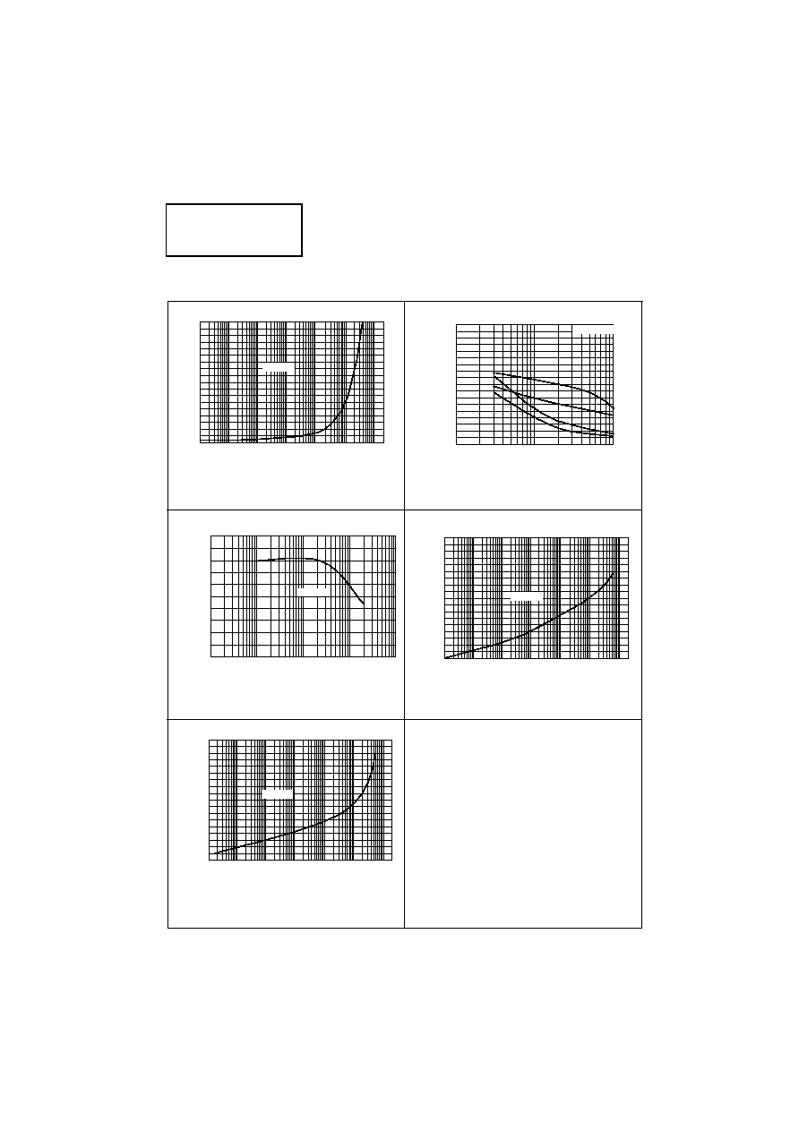
ELECTRICAL CHARACTERISTICS (at T
amb
= 25∞C unless otherwise stated).
PARAMETER
SYMBOL MIN.
TYP.
MAX.
UNIT
CONDITIONS.
Collector-Base
Breakdown Voltage
V
(BR)CBO
-80
V
I
C
=-100
µ
A, I
E
=0
Collector-Emitter
Breakdown Voltage
V
(BR)CEO
-60
V
I
C
=-10mA, I
B
=0*
Emitter-Base
Breakdown Voltage
V
(BR)EBO
-5
V
I
E
=-100
µ
A, I
C
=0
Collector Cutoff
Current
I
CBO
-0.1
-10
µ
A
µ
A
V
CB
=-60V
V
CB
=-60V,
T
amb
=100∞C
Emitter Cutoff Current
I
EBO
-0.1
µ
A
V
EB
=-4V, I
E
=0
Collector-Emitter
Saturation Voltage
V
CE(sat)
-0.15
-0.28
-0.3
-0.5
V
V
I
C
=1A, I
B
=-100mA*
I
C
=2A, I
B
=-200mA*
Base-Emitter
Saturation Voltage
V
BE(sat)
-0.9
-1.25
V
I
C
=1A, I
B
=-100mA*
Base-Emitter
Turn-On Voltage
V
BE(on)
-0.8
-1
V
I
C
=-1A, V
CE
=-2V*
Static Forward Current
Transfer Ratio
h
FE
70
100
80
40
200
200
170
80
300
I
C
=-50mA, V
CE
=-2V*
I
C
=-500mA, V
CE
=-2V*
I
C
=-1A, V
CE
=-2V*
I
C
=-2A, V
CE
=-2V*
Transition Frequency
f
T
100
140
MHz
I
C
=-100mA, V
CE
=-5V
f=100MHz
Output Capacitance
C
obo
30
pF
V
CB
=-10V f=1MHz
Switching Times
t
on
40
ns
I
C
=-500mA, V
CC
=-10V
I
B1
=I
B2
=-50mA
t
off
450
ns
*Measured under pulsed conditions. Pulse width=300
µ
s. Duty cycle
2%
ZDT751