 | –≠–ª–µ–∫—Ç—Ä–æ–Ω–Ω—ã–π –∫–æ–º–ø–æ–Ω–µ–Ω—Ç: ZHCS2000 | –°–∫–∞—á–∞—Ç—å:  PDF PDF  ZIP ZIP |
1
ZXSC100
DESCRIPTION
T h e Z X S C 1 0 0 s e r i e s i s d e s i g n e d f o r D C - D C
applications where step-up voltage conversion from
very low input voltages is required. These applications
mainly operate from single nickel cadmium or nickel
metal hydride battery cells.
The ZXSC100 devices are non-synchronous PFM,
DC-DC controller ICs which drive an external
transistor. Zetex SuperSOT4
TM
switching transistors,
with saturation resistance as low as 13m
, are
recommended as the external switching element.
These bipolar transistors are the best switching
devices available for this type of DC-DC conversion,
enabling high efficiency conversion with input
voltages down to below 1 volt.
The circuit can start up under full load with regulation
maintained down to an input voltage of only 0.926
volts. The solution configuration ensures optimum
efficiency over a wider range of load currents, several
circuit configurations are possible with power
dissipation up to 2W. The step up output voltage is
easily programmed with external resistors, the
non-synchronous architecture and SuperSOT4TM
device enabling an output voltage down to the input
voltage level. For best performance the ZXSC100
quiescent current is a small 150µA ensuring minimum
battery drain in no load conditions.
For the best in space saving the ZXSC100 is offered in
the MSOP8 package, however the devices are also
available in SO8 packaging for applications where
space saving is not so critical.
The IC and discrete combination offers the ultimate
cost vs performance solution for single cell DC-DC
conversion.
SINGLE CELL DC-DC CONVERTER SOLUTION
FEATURES
∑
SuperSOT4TM switching transistor
ZXT14N20DX:V
CE(sat)
45mV max @ 1A load
∑
Efficiency maintained over a wide range of input
voltages and load currents
82% efficiency @ V
BATT
=1V
∑
Startup under full load
∑
Minimum operating input voltage V
BATT
=0.926V
∑
Adjustable output voltage down to V
BATT
∑
Quiescent current typically 150µA referred to
input voltage
∑
MSOP8 Package
∑
SO8 Package
∑
Demonstration boards available
APPLICATIONS
∑
Cordless Telephones
∑
MP3 Players
∑
PDA
∑
Pagers
∑
Battery Backup Supplies
∑
Electronic toothbrush
∑
GPS Receivers
∑
Digital Camera
∑
Palmtop Computers
APPLICATIONS(continued)
∑
Hand Held Instruments
∑
Portable Medical Equipment
∑
Solar Powered Equipment
∑
LED Flashlight
∑
LED Backlight
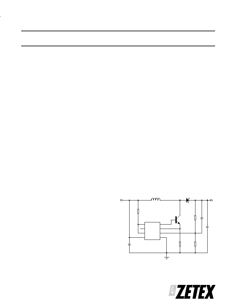
Q1
ZXT14N20DX
R2
R1
L1
D1
ZHCS2000
R3
R4
C2
C1
3.3V/0.1A
BAS
EM
RE
V
BATT
V
CC
G
ND
FB
I
SENSE
V
DRIVE
U1
ZXSC100
C3
TYPICAL APPLICATION CIRCUIT
ISSUE 1 - JANUARY 2001
ISSUE 1 - JANUARY 2001
ZXSC100
2
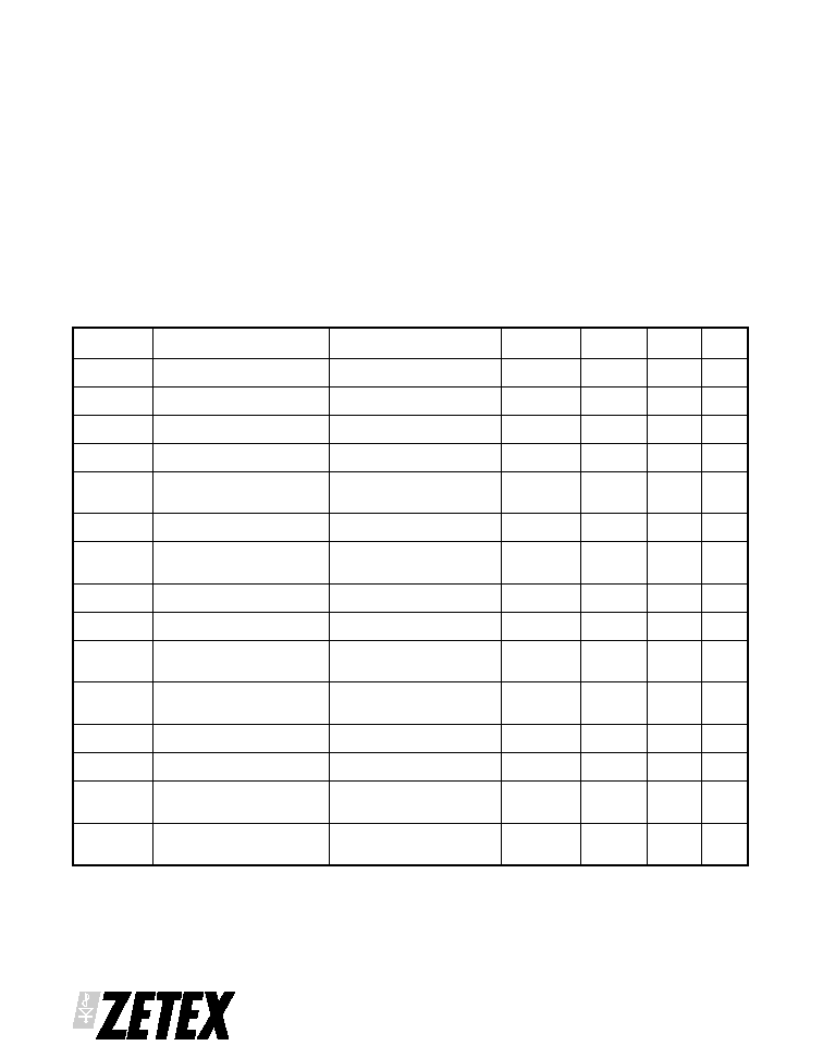
ABSOLUTE MAXIMUM RATING
ELECTRICAL CHARACTERISTICS TEST CONDITIONS (Unless otherwise stated)
V
CC
=1.2V, T
A
= 25∞C
Supply Voltage
0.3 to 3.5V
Maximum Voltage Other Pins
0.3 to V
CC
+0.3V
Power Dissipation
MSOP8
500mW
SO8
780mW
Operating Temperature
0 to 70∞C
Storage Temperature
-55 to 125∞C
Junction Temperature
150∞C
Symbol
Parameter
Conditions
Min
Typ
Max
Units
I
CC
Quiescent current
Not switching
150
200
µA
I
DRIVE
Base drive current
V
RE
= V
CC
5
10
mA
V
DRIVE
V
DRIVE
o/p voltage
V
RE
= V
CC
, I
DRIVE
= 5mA
V
CC
- 0.17
V
V
FB
Feedback voltage
708
730
752
mV
V
ISENSE
Output current
reference voltage
12
17.5
24
mV
T
CVISENSE
I
SENSE
voltage temp co.
0.4
%/∞C
V
DREF
Drive current reference
voltage
Measured with respect
to V
CC
20
30
40
mV
T
CVDREF
V
DREF
temp co.
1
%/∞C
V
CC(SRT)
Startup voltage
Any output load
1.01
1.06
1.1
V
V
CC(min)
Minimum operating
input voltage
0.926
0.98
1
V
V
CC(hys)
Supply start up to
shutdown hysteresis
80
mV
I
FB
Feedback input current
100
200
nA
I
ISENSE
I
SENSE
input current
V
ISENSE
= 0V
3
4
5.5
µA
V
O(min)
Minimum Output
Voltage
V
CC
V
V
O(max)
Maximum Output
Voltage
ZXT14N20DX as pass
element
1
20
V
1
Depends on breakdown voltage of pass device. See ZXT14N20DX data sheet
ZXSC100
ISSUE 1 - JANUARY 2001
3
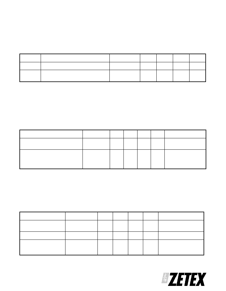
ELECTRICAL CHARACTERISTICS: AC PARAMETERS
2
TEST CONDITIONS (Unless otherwise stated) )
V
CC
=1.2V, T
A
= 25∞C
Symbol
Parameter
Conditions
Min
Typ
Max
Units
T
OFF
Discharge Pulse Width
1.7
3
4
µs
F
OSC
Recommended operating
frequency
3
200
kHz
2
These parameters guaranteed by Design
3
Operating frequency is application circuit dependant. See applications section
ZXT14N20DX
For the circuits described in the applications section, Zetex ZXT14N20DX is the recommended pass transistor.
The following indicates outline data for the ZXT, more detailed information can be found in the Zetex SuperSOT4
data book or at www.zetex.com
ELECTRICAL CHARACTERISTICS (at T
A
= 25∞C unless otherwise stated).
PARAMETER
SYMBOL
MIN.
TYP.
MAX.
UNIT
CONDITIONS.
Collector-Emitter Breakdown
Voltage
V
(BR)CEO
20
30
V
I
C
=10mA*
Collector-Emitter Saturation
Voltage
V
CE(sat)
4.5
30
75
6
45
95
mV
mV
mV
I
C
=0.1A, I
B
=10mA*
I
C
=1A, I
B
=10mA*
I
C
=4A, I
B
=40mA*
*Measured under pulsed conditions. Pulse width=300
µ
s. Duty cycle
2%
ZHCS2000
For the circuits described in the applications section Zetex ZHCS2000 is the recommended Schottky diode. The
following indicates outline data for the ZHCS, more detailed information is available at www.zetex.com
ELECTRICAL CHARACTERISTICS (at T
amb
= 25∞C unless otherwise stated).
PARAMETER
SYMBOL
MIN.
TYP.
MAX.
UNIT
CONDITIONS.
Forward Voltage
V
F
385
500
mV
mV
I
F
=1A
I
F
=2A
Reverse Current
I
R
300
µ
A
V
R
=30V
Reverse Recovery
Time
t
rr
5.5
ns
Switched from I
F
=
500mA to I
R
= 500mA.
Measured at I
R
=50mA
*Measured under pulsed conditions. Pulse width=300
µ
s. Duty cycle
2%
3

ISSUE 1 - JANUARY 2001
ZXSC100
4
TYPICAL CHARACTERISTICS
ZXSC100
ISSUE 1 - JANUARY 2001
5
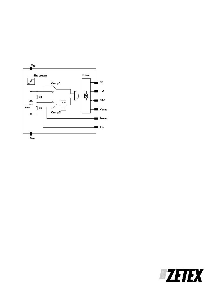
DEVICE DESCRIPTION
The ZXSC100 is non-synchronous PFM, DC-DC
controller IC which, when combined with a high
performance external transistor, enables the
production of a high efficiency boost converter for use
in single cell applications. A block diagram is shown
for the ZXSC100 in Figure 1.
A shutdown circuit turns the device on or off at V
CC
=1V
with a hysteresis of typically 80mV. At start up,
comparator Comp1 turns the driver circuit and
therefore the external switching transistor on. This
circuit will remain active until the feedback voltage at
the pin FB rises above V
REF
, which is set to 730mV. An
external resistive divider on the FB pin sets the output
voltage level.
Comparator Comp2 forces the driver circuit and the
external switching transistor off, if the voltage at
I
SENSE
exceeds 25mV. The voltage at I
SENSE
is taken
from a current sense resistor connected in series with
the emitter of the switching transistor.
A monostable following the output of Comp2 extends
the turn-off time of the output stage by a minimum of
2us. This ensures that there is sufficient time to
discharge the inductor coil before the next on period.
The AND gate between the monostable and Comp1
output ensures that the switching transistor always
remains on until the I
SENSE
threshold is reached and
that the minimum discharge period is always
asserted. The pulse width is constant, the pulse
frequency varies with the output load.
The driver circuit supplies the external switching
transistor with a defined
current, which is
programmed by an external resistor connected
between the RE pin and V
CC
. The internal reference
voltage for the circuit is 25mV below V
CC
. To maximise
efficiency the external transistor is switched quickly,
typically being forced off within 20ns.
In higher power applications more current can be
supplied to the switching transistor by using a further
external component. The driver transistor in the IC can
be bypassed with the addition of a discrete PNP. More
information on this circuit configuration can be found
in the applications section.
Figure 1
ZXSC100 Block Diagram