DUAL POLARISATION SWITCH TWIN LNB
MULTIPLEX CONTROLLER
ISSUE 1- NOVEMBER 1998
DEVICE DESCRIPTION
The ZLNB101 dual polarisation switch
controller is one of a wide range of satellite
receiver LNB support circuits. It features two
completely independent channels, each
providing two logic outputs under the
control of a voltage sensitive input. It is
intended for use in Twin LNB designs,
replacing many dIscrete components to save
both manufacturing cost and PCB size whilst
improving reliability.
The two inputs of the ZLNB101 have a
nominal threshold of 14.5V. Their threshold
is temperature compensated to minimise
drift. Each features a low and stable input
current that enables transient protection to
be achieved with the addition of only a single
resistor per channel.
Normal and an inverted outputs are
provided for each input. All outputs can
source 15mA and sink 10mA making them
suitable to drive TTL and CMOS logic, pin
diodes and for IF-amp supply switching.
The ZLNB101 operates from a single supply
of between 5-12V. Its quiescent current is
typically only 4mA and this does not change
significantly with load or logic state. It is
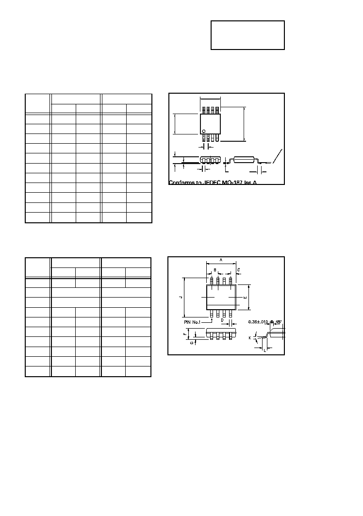
available in either the standard SO8 or space
saving MSOP8 surface mount packages.
Device operating temperature is -40∞C to
+85∞C to suit a wide range of environmental
conditions.
FEATURES
∑
provides polarity detection and control
∑
transient resistant
∑
low input current
∑
low supply current
∑
temperature compensated input
threshold
∑
standard and inverted output available
simultaneously wide supply operating
range
∑
dual polarisation switch
∑
eliminates external components
∑
simplifies design
APPLICATIONS
∑
twin LNBs
∑
IF switch box
∑
LNB switch boxes
ZLNB100
75

ABSOLUTE MAXIMUM RATINGS
Supply Voltage
-0.6V to 15V
Supply Current
50mA
V
POL1
and V
POL2
Input Voltage
25V Continuous
Operating Temperature
-40 to 85∞C
Storage Temperature
-40 to 85∞
Power Dissipation (T
amb
=
25∞C)
SO8
500mW
MSOP8
500mW
ELECTRICAL CHARACTERISTICS TEST CONDITIONS (Unless otherwise stated):
T
amb
=
25∞C,V
CC
=5V,I
D
=10mA (R
CAL1
=33k
)
SYMBOL PARAMETER
CONDITIONS
LIMITS
UNITS
Min
Typ
Max
V
CC
Supply Voltage
5
12
V
I
CC
Supply Current
All inputs and outputs open circuit
I
VERT1
= I
VERT2
= 10mA, V
POL1
=
V
POL2
= 14V
I
HOR1
= I
HOR2
= 10mA, V
POL1
=
V
POL2
= 15.0V
10
30
30
mA
mA
mA
V
POL1
and V
POL2
Inputs
I
POL
Current
V
POL1
= V
POL2
= 25V (Note 4)
10
20
40
µ
A
V
TPOL
Threshold
Voltage
(Note 1) (Note 4)
14.0
14.5
15.0
T
SPOL
Switching Speed
100
µ
s
V
VHIGH
V
VHIGH
V
VHIGH
V
VLOW
Vert 1/2 Outputs
Voltage High
Voltage High
Voltage High
Voltage Low
I
VERT1
=I
VERT2
=10mA,
V
POL1
= V
POL2
= 14V
I
VERT1
=I
VERT2
=15mA,
V
POL1
= V
POL2
= 14V
I
VERT1
=I
VERT2
=10
µ
A,
V
POL1
= V
POL2
= 14V
I
VERT1
=I
VERT2
=-10mA,
V
POL1
= V
POL2
= 15.0V
V
CC
-1.0
V
CC
-1.2
V
CC
-0.2
0
V
CC
-0.8
V
CC
-0.9
V
CC
-0.1
0.25
V
CC
V
CC
V
CC
0.5
V
V
V
V
V
VHIGH
V
VHIGH
V
VHIGH
V
VLOW
Hor 1/2 Outputs
Voltage High
Voltage High
Voltage High
Voltage Low
I
HOR1
=I
HOR2
=10mA,
V
POL1
= V
POL2
= 15.0V
I
HOR1
=I
HOR2
=15mA,
V
POL1
= V
POL2
= 15.0V
I
HOR1
=I
HOR2
=10
µ
A,
V
POL1
= V
POL2
= 15.0V
I
HOR1
=I
HOR2
=-10mA,
V
POL1
= V
POL2
= 14V
V
CC
-1.0
V
CC
-1.2
V
CC
-0.2
0
V
CC
-0.8
V
CC
-0.9
V
CC
-0.1
0.25
V
CC
V
CC
V
CC
0.5
V
V
V
V
ZLNB100
76
Note:-
1) V
POL1
and V
POL2
switching thresholds apply over the whole operating temperature range
specified above.
2) Inputs V
POL1
and V
POL2
are designed to be wired to the power input of an LNB via high value
(10k) resistors. Input V
POL1
controls outputs Vert1 and Hor1. Input V
POL2
controls outputs Vert2
and Hor2. With either input voltage set at or below 14V, the corresponding Vert pin will be high
and Hor pin low. With either input voltage at or above 15.0V, the corresponding Vert pin will be
low and Hor pin high. Any input or output not required may be left open-circuit.
3) All outputs are designed to be compatible with TTL, CMOS, pin diode and IF Amp loads.
4) Applied via 10k resistors
77
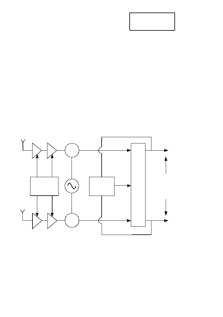
Bias Generator
ZNBG40XX
Series
ZLNB100 Series
Dual H/V Switch
Vertical
Antenna
Horizontal
Antenna
Gain Stage
GaAs/HEMTFET
Gain Stage
GaAs/HEMTFET
1
4
2
IF down feed
950-1750 MHz
- Standard Band
950-2050 MHz
- Enhanced Band
+
+
Mixer
Mixer
H/V Output 2
H/V Output 1
3
Control Input
<=13V-Horizontal
>=14.5V-Vertical
Control
Horizontal
Vertical
PIN
Diode
MUX
DC Input
13-25V
The following block diagram shows a typical block diagram twin LNB design. The ZLNB100
provides the two polarity switches required to decode the two independent receiver feeds.
Additionally the front end bias requirements of the LNB are provided by the ZNBG4000 or
ZNBG6000 offering a very efficient and cost effective solution.
ZLNB100