DUAL TONE and POLARITY SWITCH LNB
MULTIPLEX CONTROLLER
ISSUE 1- NOVEMBER 1998
DEVICE DESCRIPTION
The ZLNB200X dual polarisation and tone
switch controller is one of a wide range of
satellite receiver LNB support circuits
available from Zetex. It features two
completely independent channels, each
providing logic outputs to control LNB
polarisation selection, local oscillator
selection and downfeed disable. It is
intended for use in Twin Universal LNBs,
replacing many discrete components to save
both manufacturing cost and PCB size whilst
improving reliability.
The two polarisation control inputs of the
ZLNB200X have a nominal threshold of
14.75V. The threshold is temperature
compensated to minimise drift. Each
features a low and stable input current that
enables transient protection to be achieved
with the addition of only a single resistor per
channel.
Twin Universal LNBs can be called to
operate with one of their controlling
receivers powered down/disconnected, with
attendant cable mismatch problems. To
e as e de si gn f or this situation, each
polarisation input of the ZLNB200X has a
second threshold set at 9.5V. An input
voltage below this threshold indicates
"receiver not present", switching the
channels Enable pin low. This logic output
can be used to disable the associated
downfeed driver, eliminating any problems
due to cable mismatch.
Universal LNB local oscillator selection is
achieved by detection of a low level AC
voltage superimposed on the polarisation
control voltage. To facilitate this function,
the ZLNB200X includes a separate tone
detector for each channel. Full control of
detector bandwidth and sensitivity is
provided using two external resistors and
capacitors. In the ZLNB2003/4, additional
control of tone switch delays is provided to
assist with the rejection of low frequency
control signals intended for other systems.
Polarisation switch and tone detector
outputs can source and sink 10mA making
them suitable to drive TTL and CMOS logic,
pin diodes and for IF-amp supply switching.
The ZLNB200X operates from a single
supply which can be anything from 5-10V. Its
quiescent current is typically only 6mA and
this does not change significantly with load
or logic state. It is available in the space
saving QSOP16 surface mount package.
FEATURES
∑
Dual polarisation switch
∑
Temperature compensated polarisation
switch threshold
∑
Transient resistant inputs
∑
Includes Receiver-Off detector
∑
Dual tone switch
∑
User adjustable filter centre frequency
and bandwidth
∑
User adjustable tone switching delays
(ZLNB2003/4 only)
∑
Tone and pol. outputs TTL, CMOS, Pin
diode and IF amp capable
∑
Receiver-Off detector TTL and CMOS
compatible
∑
Wide supply operating range
∑
Low quiescent current
∑
Few external components
∑
Eliminates many discrete components
APPLICATIONS
∑
Twin Universal LNB
∑
Twin Universal IF switch boxes
∑
LNB switch boxes
81
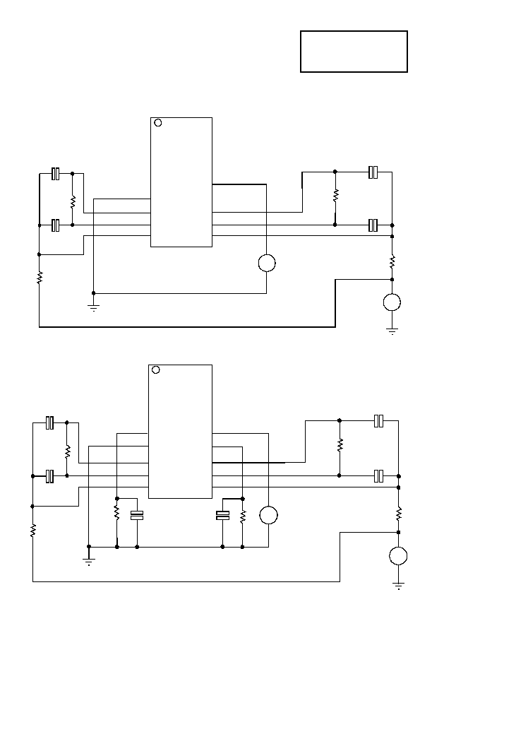
ZLNB2001 ZLNB2002
ZLNB2003 ZLNB2004
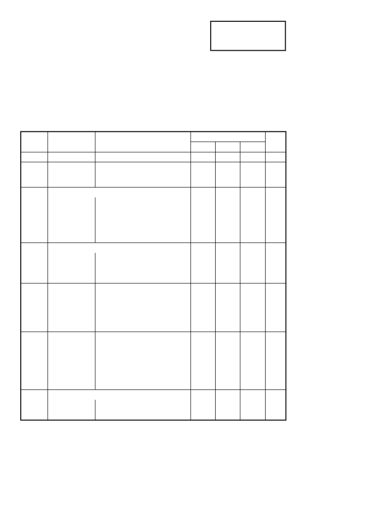
ABSOLUTE MAXIMUM RATINGS
Supply Voltage
-0.6V to 12V
Supply Current
100mA
V
POL1
and V
POL2
Input Voltage
25V Continuous
Operating Temperature
-40 to 70∞C
Storage Temperature
-40 to 85∞
Power Dissipation (T
amb
=
25∞C)
QSOP16
500mW
82
ELECTRICAL CHARACTERISTICS TEST CONDITIONS (Unless otherwise stated):
T
amb
=
25∞C,V
CC
=5V,I
D
=10mA (R
CAL1
=33k
)
SYMBOL PARAMETER
CONDITIONS
LIMITS
UNITS
Min
Typ
Max
V
CC
Supply Voltage
5
10
V
I
CC
Supply Current IHV
out1,2
=IT
out1,2
=0
IT
out1,2
=0,IHV
out1,2
=10mA,
V
POL
=15.5V
5.5
26
12
32
mA
mA
V
POL1
and V
POL2
Inputs
I
POL
Current
V
POL1
= V
POL2
= 25V (Note 2)
10
25
40
µ
A
V
TPOL
Threshold
Voltage
T
amb
=-40∞C to 70∞C (Note 2)
14.0
14.75
15.5
V
T
SPOL
Switching
Speed
100
µ
s
IHV
out1
and IHV
out2
Outputs
VHV
HIGH
Voltage High
IHV
out1,2
=-20
µ
A,V
POL1,2
= 15.5V
V
CC
-0.2 V
CC
-0.1 V
CC
V
VHV
HIGH
Voltage High
IHVout1,2=-10
µ
A,V
POL1,2
= 15.5V V
CC
-1.0 V
CC
-0.9 V
CC
V
VHV
LOW
Voltage Low
IHV
out1,2
=-10
µ
A,V
POL1,2
= 14V
0
0.29
0.5
V
Enable 1,2
Outputs
VEN
HIGH
Voltage High
IEnable1,2=-100
µ
A,V
POL1,2
= 10V V
CC
-1.0 V
CC
-0.75 V
CC
V
VEN
HIGH
Voltage High
IEnable1,2=20
µ
A,V
POL1,2
= 8.0V
0
0.14
V
CC
V
VEN
LOW
Voltage Low
IEnable1,2=500
µ
A,V
POL1,2
=8.0V
0
0.25
0.5
V
Filter Amplifier
I
B
Input Bias
Current
RF1=150k
0.02
0.07
0.25
µ
A
V
out
V
out
(Note 1)
RF1=150k
1.75
1.95
2.15
V
I
out
I
out
(Note 1)
Vout=1.96V, Vfin=2.1V
400
520
650
µ
A
G
V
Voltage Gain
F=22kHz, Vin=1mV
0
46
dB
Rectifier (ZLNB2003 and ZLNB2004 ONLY)
V
REC
Vout (Note 1)
RF1=150k, IL=10
µ
A
1.8
2.0
2.2
V
ILeakage
RF1=150k, Vout=3V (Note 1)
20
200
nA
ZLNB2001 ZLNB2002
ZLNB2003 ZLNB2004
SYMBOL PARAMETER
LIMITS
UNITS
Min
Typ
Max
Comparator (ZLNB2003 and ZLNB2004 ONLY)
V
TH
Threshold
(Note 1)
F=0
2.95
3.2
3.45
V
V
VHIGH
V
VHIGH
V
VLOW
Tout 1/2
Outputs
Voltage High
Voltage High
Voltage Low
ITout1,2=-20
µ
A, Test Circuit 1,
Tone enabled
ITout1,2=-10mA, Test Circuit 1,
Tone enabled
ITout1,2=10mA, Test Circuit 1,
Tone disabled
V
CC
-0.2
V
CC
-1.0
0
V
CC
-0.1
V
CC
-0.9
0.29
V
CC
V
CC
0.5
V
V
V
Note:-
1) The parameters Filter Amplifier Vout, Iout, Rectifier Vout and Comparator Threshold Voltage
are all directly (linearly) related to Vcc.
2) Applied via 10k resistors
ELECTRICAL CHARACTERISTICS TEST CONDITIONS (Unless otherwise stated):
T
amb
=
25∞C,V
CC
=5V,I
D
=10mA (R
CAL1
=33k
)
ZLNB2001 ZLNB2002
ZLNB2003 ZLNB2004
83
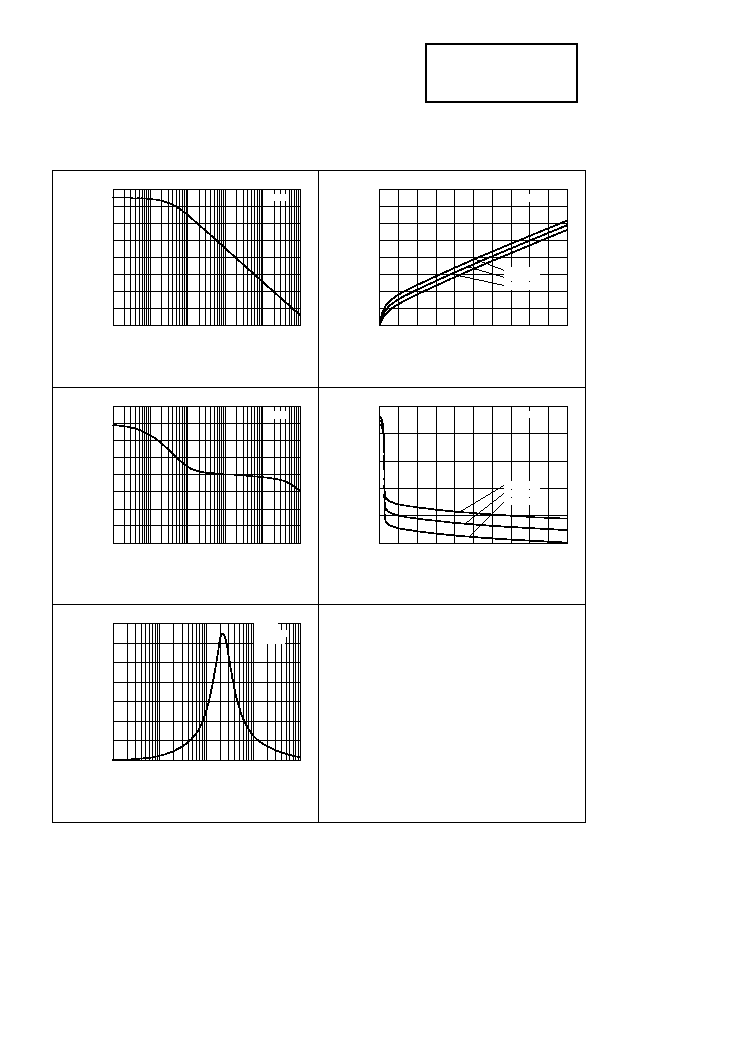
Filter Response
100
1k
10k
100k
1M
0
0.2
0.4
0.6
0.8
1.0
Frequency (Hz)
Fo
ut
V
o
l
t
ag
e (
V
p/
p)
1.2
1.4
Open Loop Phase v Frequency
100
1k
10k
100k
1M
0
30
60
90
120
Frequency (Hz)
O
p
en L
o
o
p
P
h
ase (
D
eg
r
e
es)
150
180
10M
HV/Tout Voltage High v Load Current
0
2
4
6
8
4.2
4.4
4.6
Load Current (mA)
H
V
/T
ou
t V
o
lt
ag
e
Hig
h
(V)
4.8
10
4.0
5.0
HV/Tout Voltage Low v Load Current
0
2
4
6
8
0
0.1
0.2
Load Current (mA)
H
V
/
T
ou
t
V
o
l
t
ag
e Low
(
V
)
0.3
10
0.4
Open Loop Gain v Frequency
100
1k
10k
100k
1M
0
10
20
30
40
Frequency (Hz)
O
p
en
Lo
op
G
a
i
n
(
d
B
)
50
60
70
10M
Vcc = 5V
Vin=0.1Vp/p
Test Circ. 1
Vcc = 5V
Vcc = 5V
Tamb = -40∞C
Tamb = 25∞C
Tamb = 70∞C
Vcc = 5V
Tamb = -40∞C
Tamb = 25∞C
Tamb = 70∞C
Vcc = 5V
TYPICAL CHARACTERISTICS
ZLNB2001 ZLNB2002
ZLNB2003 ZLNB2004
85