 | –≠–ª–µ–∫—Ç—Ä–æ–Ω–Ω—ã–π –∫–æ–º–ø–æ–Ω–µ–Ω—Ç: ZMR500C | –°–∫–∞—á–∞—Ç—å:  PDF PDF  ZIP ZIP |
FIXED 2.5 AND 5 VOLT
MINIATURE VOLTAGE REGULATORS
ISSUE 4 - MARCH 2002
DEVICE DESCRIPTION
The ZMR series of three terminal fixed
positive voltage regulators feature internal
current limit and will shut down under
thermal overload conditions making the
devices difficult to destroy.
The circuit design offers an exceptionally
low quiescent current, only 30
µ
A for the 2.5
volt device, ideal for low power applications.
The initial devices in the series regulate to
2.5 or 5 volts with a drive capability up to
50mA, however, the flexible design will
allow other voltage selections to be made.
The device is designed with space saving in
mind and is available in the small outline
SOT23 package. The device is also available
in through hole TO92 package.
FEATURES
∑
Small outline SOT23 package
∑
TO92 package
∑
2.5V and 5V output
∑
22.5V maximum input voltage
(ZMR25H)
∑
25V maximum input voltage (ZMR50H)
∑
Output current up to 50mA
∑
Very low Quiesent current (30
µ
A)
∑
Unconditionally stable
∑
Other output voltages possible
∑
Internal short circuit current limit
VOLTAGE RANGE
ZMR250 2.5V
ZMR500
5.0V
ZMR25H
2.5V
ZMR50H
5.0V
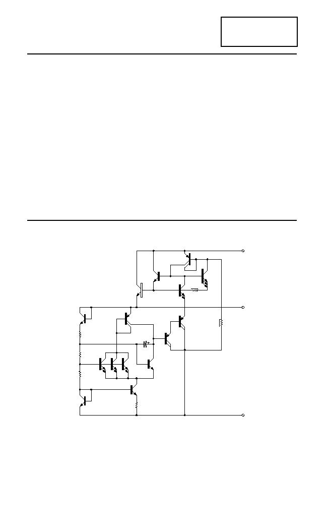
Vin
Vout
Gnd
SCHEMATIC DIAGRAM
ZMR SERIES
4-104
ABSOLUTE MAXIMUM RATINGS
Input voltage (ZMR25H)
22.5V
ZMR250 20V
(ZMR50H)
25V
ZMR500 20V
Package power dissipation
SOT23 500mW (Note 3)
(T
amb
=25 ∞C)
TO92 600mW
Output current (I
O
)
100mA
Operating temperature
-55 to 125∞C
Storage temperature
-65 to 150∞C
Note:
1. The maximum operating input voltage and output current of the device will be governed by
the maximum power dissipation of the selected package. Maximum package power dissipation
is specified at 25 ∞C and must be linearly derated to zero at T
amb
=125∞C.
2. The following data represents pulse test conditions with junction temperatures as indicated at
the initiation of the test. Continuous operation of the devices with the stated conditions might
exceed the power dissipation limits of the chosen package.
3. Maximum power dissipation for the SOT23 package, is calculated assuming that the device is
mounted on a ceramic substrate measuring 15 x 15 x 0.6mm.
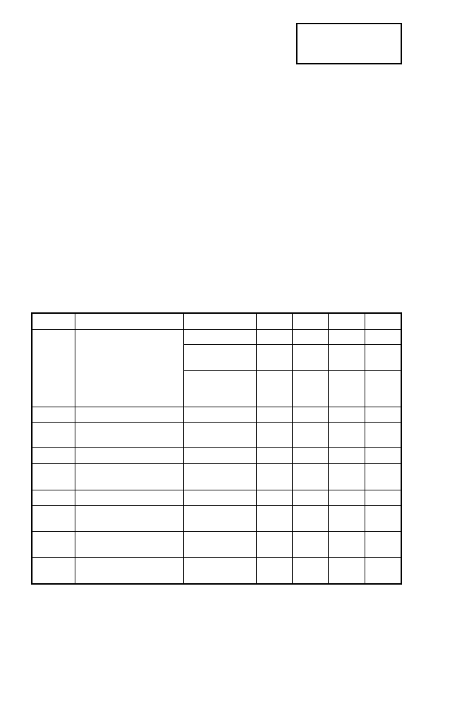
ZMR25H
ELECTRICAL CHARACTERISTICS
TEST CONDITIONS (Unless otherwise stated):T
j
=25∞C, I
O
=10mA, V
in
=6.5V
SYMBOL PARAMETER
CONDITIONS
MIN.
TYP.
MAX.
UNITS
V
O
Output Voltage
2.438
2.5
2.563
V
I
O
=0 to 50mA
T
j
=-55 to 125∞C
2.360
2.640
V
V
in
=4.5 to 22.5V
I
O
=0 to 50mA
T
j
=-55 to 125∞C
2.360
2.640
V
V
O
Line Regulation
V
in
=4.5 to 22.5V
5
15
mV
V
O
Load Regulation
I
O
=0 to 50mA
I
O
=0 to 10mA
20
12
30
mV
mV
l
s
Supply Current
T
j
=-55 to 125∞C
30
40
µ
A
l
s
Supply Current Change
I
O
=0 to 50mA
V
in
=4.5 to 22.5V
1
2
±
10
10
µ
A
µ
A
V
n
Output Noise Voltage
f=10Hz to 10KHz
65
µ
V rms
V
in
/
V
O
Ripple Rejection
V
in
=6.3 to 18V
f=120Hz
55
75
dB
V
in
Input Voltage Required
To Maintain Regulation
4.2
3.9
V
V
O
/
T
Average Temperature
Coefficient of V
O
I
O
=5.0mA
T
j
=-55 to 125∞C
0.275
0.700
mV/∞C
ZMR SERIES
4-105

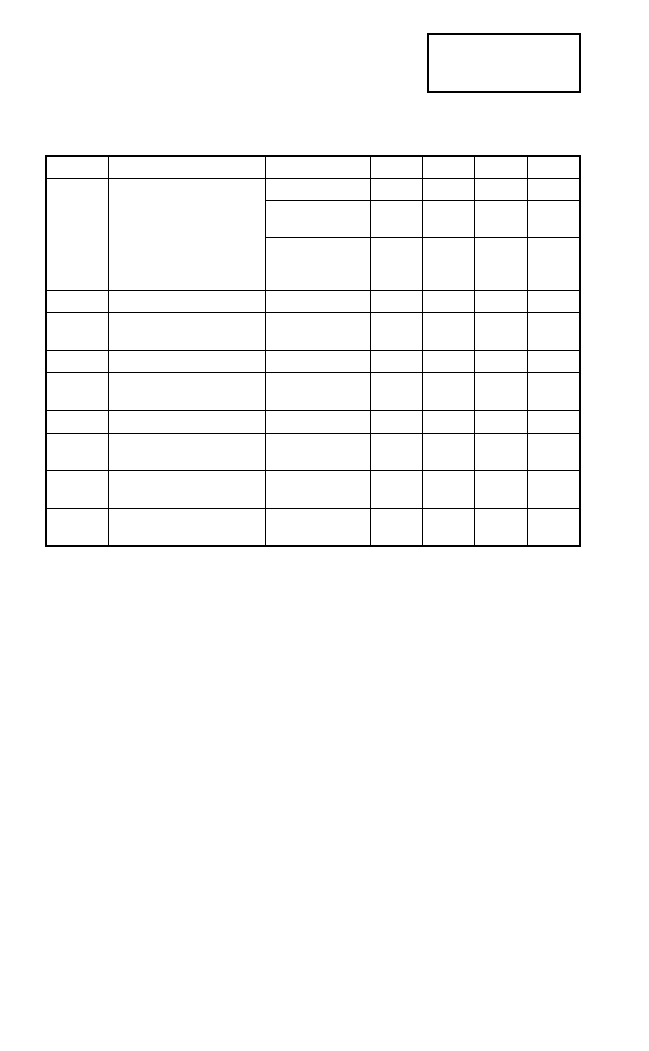
ZMR50H
ELECTRICAL CHARACTERISTICS
TEST CONDITIONS (Unless otherwise stated):T
j
=25∞C, I
O
=10mA, V
in
=10V
SYMBOL PARAMETER
CONDITIONS
MIN.
TYP.
MAX.
UNITS
V
O
Output Voltage
4.875
5
5.125
V
I
O
=0 to 50mA
T
j
=-55 to 125∞C
4.780
5.160
V
V
in
=7 to 25V
I
O
=0 to 50mA
T
j
=-55 to 125∞C
4.780
5.175
V
V
O
Line Regulation
V
in
=7 to 25V
5
15
mV
V
O
Load Regulation
I
O
=0 to 50mA
I
O
=0 to 10mA
25
15
40
mV
mV
l
s
Supply Current
T
j
=-55 to 125∞C
50
70
µ
A
l
s
Supply Current Change
I
O
=0 to 50mA
V
in
=7 to 25V
1
2
±
10
10
µ
A
µ
A
V
n
Output Noise Voltage
f=10Hz to 10KHz
90
µ
V rms
V
in
/
V
O
Ripple Rejection
V
in
=8 to 18V
f=120Hz
55
72
dB
V
in
Input Voltage Required
To Maintain Regulation
7
6.7
V
V
O
/
T
Average Temperature
Coefficient of V
O
I
O
=5.0mA
T
j
=-55 to 125∞C
0.275
0.700
mV/∞C
ZMR SERIES
4-106
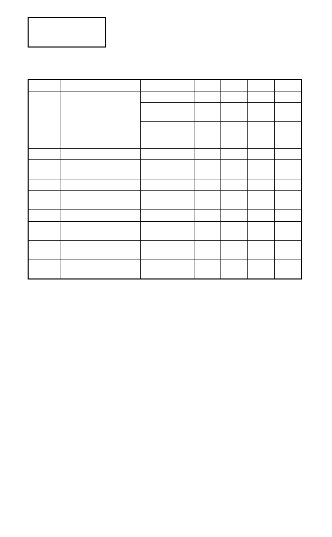
ZMR250
ELECTRICAL CHARACTERISTICS
TEST CONDITIONS (Unless otherwise stated):T
j
=25∞C, I
O
=10mA, V
in
=6.5V
SYMBOL PARAMETER
CONDITIONS
MIN.
TYP.
MAX.
UNITS
V
O
Output Voltage
2.438
2.5
2.563
V
I
O
=0 to 50mA
T
j
=-55 to 125∞C
2.360
2.640
V
V
in
=4.5 to 20V
I
O
=0 to 50mA
T
j
=-55 to 125∞C
2.360
2.640
V
V
O
Line Regulation
V
in
=4.5 to 20V
5
15
mV
V
O
Load Regulation
I
O
=0 to 50mA
I
O
=0 to 10mA
20
12
30
mV
mV
l
s
Supply Current
T
j
=-55 to 125∞C
30
40
µ
A
l
s
Supply Current Change
I
O
=0 to 50mA
V
in
=4.5 to 20V
1
2
±
10
10
µ
A
µ
A
V
n
Output Noise Voltage
f=10Hz to 10KHz
65
µ
V rms
V
in
/
V
O
Ripple Rejection
V
in
=6.3 to 18V
f=120Hz
55
75
dB
V
in
Input Voltage Required
To Maintain Regulation
4.2
3.9
V
V
O
/
T
Average Temperature
Coefficient of V
O
I
O
=5.0mA
T
j
=-55 to 125∞C
0.275
0.700
mV/∞C
ZMR SERIES
4-107
ZMR500
ELECTRICAL CHARACTERISTICS
TEST CONDITIONS (Unless otherwise stated):T
j
=25∞C, I
O
=10mA, V
in
=10V
SYMBOL PARAMETER
CONDITIONS
MIN.
TYP.
MAX.
UNITS
V
O
Output Voltage
4.875
5
5.125
V
I
O
=0 to 50mA
T
j
=-55 to 125∞C
4.780
5.160
V
V
in
=7 to 20V
I
O
=0 to 50mA
T
j
=-55 to 125∞C
4.780
5.175
V
V
O
Line Regulation
V
in
=7 to 20V
5
15
mV
V
O
Load Regulation
I
O
=0 to 50mA
I
O
=0 to 10mA
25
15
40
mV
mV
l
s
Supply Current
T
j
=-55 to 125∞C
50
70
µ
A
l
s
Supply Current Change
I
O
=0 to 50mA
V
in
=7 to 20V
1
2
±
10
10
µ
A
µ
A
V
n
Output Noise Voltage
f=10Hz to 10KHz
90
µ
V rms
V
in
/
V
O
Ripple Rejection
V
in
=8 to 18V
f=120Hz
55
72
dB
V
in
Input Voltage Required
To Maintain Regulation
7
6.7
V
V
O
/
T
Average Temperature
Coefficient of V
O
I
O
=5.0mA
T
j
=-55 to 125∞C
0.275
0.700
mV/∞C
ZMR SERIES
4-108
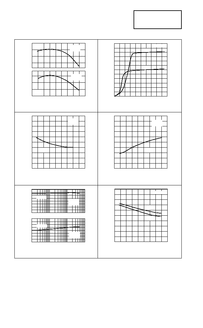
-50
-25
0
25
50
75 100 125
-50 -25
0
25
50
75 100 125
2.5
2.0
1.5
1.0
0.5
0
D
r
op
-
O
u
t
V
o
l
t
ag
e
(
V
)
Drop-Out Voltage v Temperature
Quiescent Current v Temperature
-50
-25
0
25
50
75 100 125
Temperature (∞C)
Output Voltage Temperature
0
20
40
2
4
6
8
10 12
14
16
18
20
60
10
30
50
Input Voltage (V)
Quiescent Current v Voltage
28
0.1
1
10
100
27
29
47
48
49
50
30
75
Quiescent Current v Temperature
Qu
i
e
sce
n
t
C
u
r
r
e
n
t
(µ
A
)
-50 -25
26
28
0
25
50
32
30
34
125
100
40
44
48
52
56
60
Output Current
Temperature (∞C)
Temperature (∞C)
Temperature (∞C)
5.00
5.02
4.98
4.96
2.50
2.48
2.46
2.52
ZMR50H
ZMR25H
O
u
t
p
ut
V
o
lt
a
g
e
Quiescent Current v Output Current
I
o
=5mA
V
in
=V
o
+4
I
o
=5mA
V
in
=V
o
+4
I
o
=10mA
I
o
=0
V
in
=V
o
+4
I
o
=0
V
in
=V
o
+4
I
o
=0
V
in
=V
o
+4
I
o
=0
V
in
=V
o
+4
I
o
=10mA
TYPICAL CHARACTERISTICS
Qu
i
e
s
c
e
n
t C
u
rre
n
t
(
µ
A)
Qu
i
e
s
c
e
n
t C
u
rre
n
t
(
µ
A)
Qu
i
e
s
c
e
n
t
Cu
rre
n
t
(µ
A)
ZMR25H
ZMR50H
ZMR25H
ZMR50H
ZMR25H
ZMR25H
ZMR50H
ZMR50H
ZMR SERIES
4-109
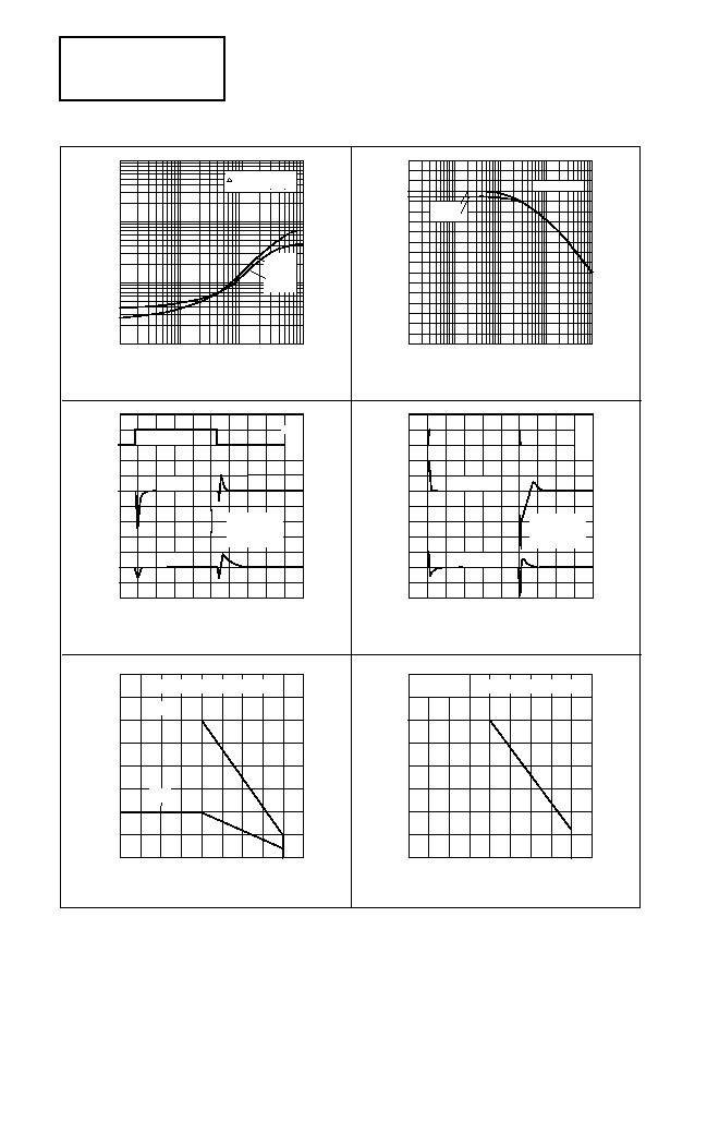
0
Time (µs)
Line Transient Response
Load Current
0
10
20
30
40
50
Time (µs)
O
u
t
p
ut
V
o
l
t
age
D
evi
at
i
o
n
(
V
)
Load Transient Response
0
10
20
30
40
50
60
70
80
90
10
100
1K
10K
100K
Ripple Frequency (Hz)
Ri
pp
l
e
Re
je
c
t
i
o
n
(
d
B)
100
1K
10K
100K
10
1.0
0.1
0.01
Frequency (Hz)
O
u
tp
ut
I
m
ped
a
n
c
e
(
)
I = 10mA
V = V + 4V
O
IN
OUT
Output Impedance v Frequency
Ripple Rejection v Ripple Frequency
ZMR50H
ZMR25H
ZMR50H
ZMR25H
ZMR25H
ZMR50H
20
40
60
80
100
0
10mA
ZMR50H
ZMR25H
Vin
0
-0.4
0
-0.4
0.4
0.4
0V
5V
0
0.4
-0.4
0
-0.4
0.4
O
u
t
p
ut
V
o
l
t
ag
e D
evi
at
i
o
n
(
V
)
0
1
2
Po
w
e
r
D
i
s
s
i
pa
tio
n
Po
w
e
r
D
i
s
s
ip
at
i
o
n
800
600
400
200
0
Power Derating
Power Derating
TO92
(m
W)
(m
W)
o
I = 2mA
-50
-25
0
25
50
75 100 125
Temperature (∞C)
-50
-25
0
25
50
75 100 125
Temperature (∞C)
Io= 10mA
SOT23
Surface Mount Devices
Through Hole Device
TYPICAL CHARACTERISTICS
C
OUT
=0
V
IN
=V
o
+4
dV
IN
/dt=5V/µs
C
OUT
=0
V
IN
=V
o
+4
dI
o
/dt=1A/µs
ZMR SERIES
4-110
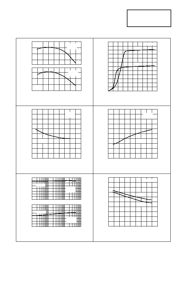
-50
-25
0
25
50
75 100 125
-50 -25
0
25
50
75 100 125
2.5
2.0
1.5
1.0
0.5
0
D
r
op
-
O
u
t
V
o
l
t
ag
e
(
V
)
Drop-Out Voltage v Temperature
Quiescent Current v Temperature
-50
-25
0
25
50
75 100 125
Temperature (∞C)
Output Voltage Temperature
0
20
40
2
4
6
8
10 12
14
16
18
20
60
10
30
50
Input Voltage (V)
Quiescent Current v Voltage
28
0.1
1
10
100
27
29
47
48
49
50
30
75
Quiescent Current v Temperature
Qu
i
e
sce
n
t
C
u
r
r
e
n
t
(µ
A
)
-50 -25
26
28
0
25
50
32
30
34
125
100
40
44
48
52
56
60
Output Current
Temperature (∞C)
Temperature (∞C)
Temperature (∞C)
5.00
5.02
4.98
4.96
2.50
2.48
2.46
2.52
ZMR500
ZMR250
O
u
t
p
ut
V
o
lt
a
g
e
Quiescent Current v Output Current
I
o
=5mA
V
in
=V
o
+4
I
o
=5mA
V
in
=V
o
+4
I
o
=10mA
I
o
=0
V
in
=V
o
+4
I
o
=0
V
in
=V
o
+4
I
o
=0
V
in
=V
o
+4
I
o
=0
V
in
=V
o
+4
I
o
=10mA
TYPICAL CHARACTERISTICS
Qu
i
e
s
c
e
n
t C
u
rre
n
t
(
µ
A)
Qu
i
e
s
c
e
n
t C
u
rre
n
t
(
µ
A)
Qu
i
e
s
c
e
n
t
Cu
rre
n
t
(µ
A)
ZMR250
ZMR500
ZMR250
ZMR500
ZMR250
ZMR250
ZMR500
ZMR500
ZMR SERIES
4-111
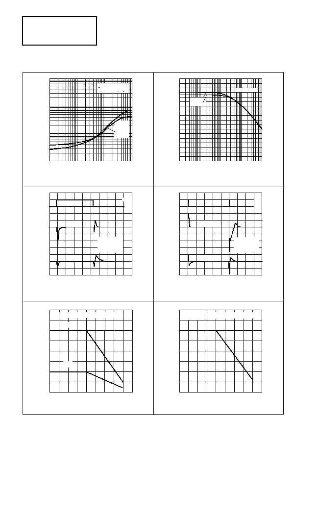
0
Time (µs)
Line Transient Response
Load Current
0
10
20
30
40
50
Time (µs)
O
u
t
p
u
t
V
o
lt
ag
e
D
evia
t
io
n
(
V
)
Load Transient Response
0
10
20
30
40
50
60
70
80
90
10
100
1K
10K
100K
Ripple Frequency (Hz)
R
i
ppl
e
R
e
je
c
t
i
on
(dB
)
100
1K
10K
100K
10
1.0
0.1
0.01
Frequency (Hz)
O
u
t
p
ut
I
m
ped
a
n
c
e (
)
I = 10mA
V = V + 4V
O
IN
OUT
Output Impedance v Frequency
Ripple Rejection v Ripple Frequency
ZMR500
ZMR250
ZMR500
ZMR250
ZMR250
ZMR500
20
40
60
80
100
0
10mA
ZMR500
ZMR250
Vin
0
-0.4
0
-0.4
0.4
0.4
0V
5V
0
0.4
-0.4
0
-0.4
0.4
O
u
t
p
u
t
V
o
lt
a
g
e D
evi
at
i
o
n
(
V
)
0
1
2
Po
w
e
r
D
i
s
s
i
p
a
t
io
n
Po
w
e
r
D
i
s
s
ip
at
i
o
n
800
600
400
200
0
Power Derating
Power Derating
TO92
(m
W)
(m
W)
o
I = 2mA
-50
-25
0
25
50
75 100 125
Temperature (∞C)
-50
-25
0
25
50
75 100 125
Temperature (∞C)
Io= 10mA
SOT23
Surface Mount Devices
Through Hole Device
TYPICAL CHARACTERISTICS
C
OUT
=0
V
IN
=V
o
+4
dV
IN
/dt=5V/µs
C
OUT
=0
V
IN
=V
o
+4
dI
o
/dt=1A/µs
ZMR SERIES
4-112
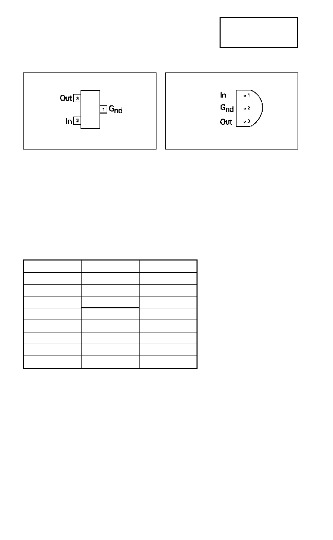
ORDERING INFORMATION
CONNECTION DIAGRAMS
Part Number
Package
Part Mark
ZMR250C
TO92
ZMR250
ZMR250F
SOT23
25K
ZMR25HC
T092
ZMR25H
ZMR25HF
SOT23
25X
ZMR500C
TO92
ZMR500
ZMR500F
SOT23
50K
ZMR50HC
TO92
ZMR50H
ZMR50HF
SOT23
5OR
TO92 Package
Suffix ≠ C
Bottom
View
SOT23 Package
Suffix ≠ F
Top
View
ZMR SERIES