
FET BIAS CONTROLLER WITH POLARISATION
SWITCH AND TONE DETECTION
ISSUE 1 - OCTOBER 1998
ZNBG3113
ZNBG3114
DEVICE DESCRIPTION
The ZNBG series of devices are designed to
meet the bias requirements of GaAs and
HEMT FETs commonly used in satellite
receiver LNBs, PMR cellular telephones etc.
with a minimum of external components.
With the addition of two capacitors and a
resistor the devices provide drain voltage and
current control for three external grounded
source FETs, generating the regulated
negative rail required for FET gate biasing
whilst operating from a single supply. This
negative bias, at -3 volts, can also be used to
supply other external circuits.
The ZNBG3113/14 includes bias circuits to
drive up to three external FETs. A control
input to the device selects either one of two
FETs as operational, the third FET is
p e r m a n e n t l y a c t i v e . T h i s f e a t u r e i s
particularly used as an LNB polarisation
switch. Also specific to LNB applications is
the 22kHz tone detection and logic output
feature which is used to enable high and low
band frequency switching.
The facility to control the tone switching
delay is provided. This allows the rejection
of other lower frequency tones tat may be
present in multiple LNB applications.
Drain current setting of the ZNBG3113/14 is
user selectable over the range 0 to 15mA, this
is achieved with addition of a single resistor.
The series also offers the choice of drain
voltage to be set for the FETs, the 3113 gives
2.2 volts drain whilst the 3114 gives 2 volts.
These devices are unconditionally stable
over the full working temperature with the
FETs in place, subject to the inclusion of the
recommended gate and drain capacitors.
These ensure RF stability and minimal
injected noise.
It is possible to use less than the devices full
complement of FET bias controls, unused
drain and gate connections can be left open
circuit without affecting operation of the
remaining bias circuits.
To protect the external FETs the circuits have
been designed to ensure that, under any
conditions including power up/down
transients, the gate drive from the bias
circuits cannot exceed the range -3.5V to 1V.
Furthermore if the negative rail experiences
a fault condition, such as overload or short
circuit, the drain supply to the FETs will shut
down avoiding excessive current flow.
The ZNBG3113/14 are available in QSOP20
for the minimum in device size. Device
operating temperature is -40 to 70∞C to suit
a wide range of environmental conditions.
FEATURES
∑
Provides bias for GaAs and HEMT FETs
∑
Drives up to three FETs
∑
Dynamic FET protection
∑
Drain current set by external resistor
∑
Regulated negative rail generator
requires only 2 external capacitors
∑
Choice in drain voltage
∑
Wide supply voltage range
∑
Polarisation switch for LNBs
∑
22KHz tone detection for band
switching
∑
Programmable tone delay
∑
Compliant with ASTRA control
specifications
∑
QSOP surface mount package
APPLICATIONS
∑
Satellite receiver LNBs
∑
Private mobile radio (PMR)
∑
Cellular telephones
4-123

ABSOLUTE MAXIMUM RATINGS
Supply Voltage
-0.6V to 12V
Supply Current
100mA
Input Voltage (V
POL
)
25V Continuous
Drain Current (per FET)
0 to 15mA
(set by R
CAL
)
Operating Temperature
-40 to 70∞C
Storage Temperature
-50 to 85∞C
Power Dissipation (T
amb
=
=
25∞C)
QSOP20
500mW
ELECTRICAL CHARACTERISTICS. TEST CONDITIONS
(Unless otherwise stated):T
amb
=
=
25∞C,V
CC
=5V,I
D
=10mA (R
CAL
=33k
)
SYMBOL PARAMETER
CONDITIONS
LIMITS
UNITS
MIN.
TYP.
MAX.
V
CC
Supply Voltage
5
10
V
I
CC
Supply Current
I
D1
to I
D3
=0
I
D1
=0,I
D2
to I
D3
=10mA, V
POL
=14V
I
D2
=0,I
D1
to I
D3
=10mA, V
POL
=15.5V
I
D1
to
I
D3
=0, I
LB
=10mA
I
D1
to
I
D3
=0, I
HB
=10mA
15
35
35
45
45
mA
mA
mA
mA
mA
V
SUB
Substrate Voltage (Internally generated) I
SUB
=0
I
SUB
=-200
µ
A
-3.5
-3.0
-2.5
-2.4
V
V
E
ND
E
NG
Output Noise
Drain Voltage
Gate Voltage
C
G
=4.7nF, C
D
=10nF
C
G
=4.7nF, C
D
=10nF
0.02
0.005
Vpkpk
Vpkpk
f
O
Oscillator
Frequency
200
350
800
kHz
ZNBG3113
ZNBG3114
4-124
SYMBOL PARAMETER
CONDITIONS
LIMITS
UNITS
MIN.
TYP.
MAX.
GATE CHARACTERISTICS
I
GO
Output Current
Range
-30
2000
µ
A
I
Dx
V
POL
I
GOx
(mA)
(V)
(
µ
µ
A)
V
G1O
V
G1L
V
G1H
Output Voltage
Gate 1 Off
Low
High
I
D1
=0
V
POL
=14
I
GO1
=-10
I
D1
=12 V
POL
=15.5 I
GO1
=-10
I
D1
=8
V
POL
=15.5 I
GO1
=0
-2.7
-2.7
0.4
-2.4
-2.4
0.75
-2.0
-2.0
1.0
V
V
V
V
G2O
V
G2L
V
G2H
Output Voltage
Gate 2 Off
Low
High
I
D2
=0
V
POL
=15.5 I
GO2
=-10
I
D2
=12 V
POL
=14
I
GO2
=-10
I
D2
=8
V
POL
=14
I
GO2
=0
-2.7
-2.7
0.4
-2.4
-2.4
0.75
-2.0
-2.0
1.0
V
V
V
V
G3L
V
G3H
Output Voltage
Gate 3 Low
High
I
D3
=12
I
GO3
=-10
I
D3
=8
I
GO3
=0
-3.5
0.4
-2.9
0.75
-2.0
1.0
V
V
DRAIN CHARACTERISTICS
I
D
Current
8
10
12
mA
I
DV
I
DT
Current Change
with V
CC
with T
j
V
CC
= 5 to 10V
T
j
=-40 to +70∞C
0.2
0.05
%/V
%/∞C
V
D1
Drain 1 Voltage:
High
ZNBG3113
ZNBG3114
I
D1
=10mA, V
POL
=15.5V
I
D1
=10mA, V
POL
=15.5V
2.0
1.8
2.2
2.0
2.4
2.2
V
V
V
D2
Drain 2 Voltage:
High
ZNBG3113
ZNBG3114
I
D2
=10mA, V
POL
=14V
I
D2
=10mA, V
POL
=14V
2.0
1.8
2.2
2.0
2.4
2.2
V
V
V
D3
Drain 3 Voltage:
High
ZNBG3113
ZNBG3114
I
D3
=10mA,
V
POL
=15.5V
I
D3
=10mA, V
POL
=15.5V
2.0
1.8
2.2
2.0
2.4
2.2
V
V
V
DV
V
DT
Voltage Change
with V
CC
with T
j
V
CC
= 5 to 10V
T
j
=-40 to +70∞C
0.5
50
%/V
ppm
I
L1
I
L2
Leakage Current
Drain 1
Drain 2
V
D1
=0.1V, V
POL
=14V
V
D2
=0.1V, V
POL
=15.5V
10
10
µ
A
µ
A
ZNBG3113
ZNBG3114
4-125
SYMBOL PARAMETER
CONDITIONS
LIMITS
UNITS
MIN.
TYP.
MAX.
TONE DETECTION CHARACTERISTICS
I
B
Filter Amplifier
Input Bias Current
R
F1
=150k
0.04
0.15
1.0
µ
A
V
OUT
Output Voltage
5
R
F1
=150k
1.75
1.95
2.05
V
I
OUT
Output Current
5
V
OUT
=1.96V, V
FIN
=2.1V
400
520
650
µ
A
G
V
Voltage Gain
f=22kHz,V
IN
=1mV
46
dB
V
OUT
Rectifier
Output Voltage
5
R
F1
=150k
I
L
=-10
µ
A
1.8
2.0
2.2
V
I
LEAK
Leakage Current
5
R
F1
=150k
V
OUT
=3V
20
200
nA
V
TH
Comparator
Threshold
Voltage
5
f=0
2.95
3.2
3.45
V
V
LOV
Output Stage
L
OV
Volt. Range
I
L
=50mA(L
B
or H
B
)
-0.5
V
CC
-1.8 V
I
LOV
L
OV
Bias Current
V
LOV
=0
0.04
0.15
1.0
µ
A
V
LBL
L
B
Output Low
V
LOV
=0
I
L
=-10
µ
A
Enabled
6
V
LOV
=3V I
L
=0
Enabled
7
-3.5
-0.01
-2.75
0
-2.5
0.01
V
V
V
LBH
L
B
Output High
V
LOV
=0
I
L
=10mA
Disabled
6
V
LOV
=3V I
L
=50mA
Disabled
7
-0.025
2.9
0
3.0
0.025
3.1
V
V
V
HBL
H
B
Output Low
V
LOV
=0
I
L
=-10
µ
A
Enabled
6
V
LOV
=3V I
L
=0
Enabled
7
-3.5
-0.01
-2.75
0
-2.5
0.01
V
V
V
HBH
H
B
Output High
V
LOV
=0
I
L
=10mA
Disabled
6
V
LOV
=3V I
L
=50mA
Disabled
7
-0.025
2.9
0
3.0
0.025
3.1
V
V
POLARITY SWITCH CHARACTERISTICS
I
POL
Input Current
V
POL
=25V (Applied via R
POL
=10k
)
10
20
40
µ
A
V
TPOL
Threshold
Voltage
V
POL
=25V (Applied via R
POL
=10k
)
14
14.75
15.5
V
T
SPOL
Switching Speed
V
POL
=25V (Applied via R
POL
=10k
)
100
ms
NOTES:
1. The negative bias voltages specified are generated on-chip using an internal oscillator. Two external capacitors, C
NB
and C
SUB
, of
47nF are required for this purpose.
2. The characteristics are measured using an external reference resistor R
CAL
of value 33k wired from pins R
CAL
to ground.
3. Noise voltage is not measured in production.
4. Noise voltage measurement is made with FETs and gate and drain capacitors in place on all outputs. C
G
, 4.7nF, are connected between
gate outputs and ground, C
D
, 10nF, are connected between drain outputs and ground.
5 . These parameters are lneearly related to V
CC
6. These parameters are measured using Test Circuit 1
7. These parameters are measured using Test Circuit 2
ZNBG3113
ZNBG3114
4-126
V2 Characteristics
Type
AC
source
Frequency
22kHz
Voltage
350mV p/p enabled
100mV p/p disabled
V2 Characteristics
Type AC
source
Frequency
22kHz
Voltage
350mV p/p enabled
100mV p/p disabled
TEST CIRCUIT 1
TEST CIRCUIT 2
ZNBG3113
ZNBG3114
4-127

JFET Drain Current v R
cal
0
20
40
60
100
0
2
4
6
8
10
R
cal
(k)
80
12
14
16
JFET Drain Voltage v Drain Current
2
4
6
8
16
2.0
2.1
2.2
Drain Current (mA)
10
2.3
2.4
12
14
V
sub
v External Load
0
0.2
0.4
0.6
1.0
-3.0
-2.5
-2.0
-1.5
-1.0
External Vsub Load (mA)
0.8
-0.5
0.0
TYPICAL CHARACTERISTICS
Vcc = 5V
Vcc = 5V
6V
8V
10V
Vcc = 5V
6V
8V
10V
Note:- Operation with loads > 200µA
is not guaranteed.
ZNBG3113
ZNBG3114
4-128
Filter Response
100
1k
10k
100k
1M
0
0.2
0.4
0.6
0.8
1.0
Frequency (Hz)
1.2
1.4
Stability Boundary
10nF
100nF
1.0
LB/HB Load Capacitance
10
1uF
0.1
100
1nF
100pF
10pF
Stable region
Open Loop Phase v Frequency
100
1k
10k
100k
1M
0
30
60
90
120
Frequency (Hz)
150
180
10M
LB/HB Dropout Voltage v Load Current
0
10
20
30
40
1.3
1.4
1.5
1.6
1.7
Load Current (mA)
1.8
1.9
50
1.2
2.0
LB/HB Offset Voltage v Load Current
0
10
20
30
40
-8
-6
-4
-2
Load Current (mA)
0
2
50
4
Open Loop Gain v Frequency
100
1k
10k
100k
1M
0
10
20
30
40
Frequency (Hz)
50
60
70
10M
V
CC
= 5V
V
IN
=0.1Vpkpk
Test Circuit 1
V
CC
= 5V
V
CC
= 5V
V
CC
= 5V
Tamb = -40 C
T
amb
= 25∞C
T
amb
= 70∞C
V
CC
= 5V
T
amb
= -40∞C
T
amb
= 25∞C
T
amb
= 70∞C
V
LOV
= 0V
Vcc = 5V
TYPICAL CHARACTERISTICS
Unstable Region
ZNBG3113
ZNBG3114
4-129
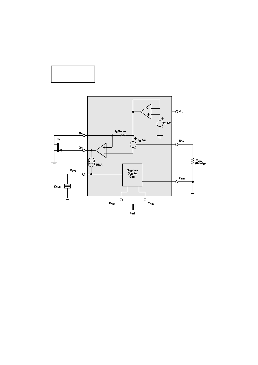
FUNCTIONAL DIAGRAM
FUNCTIONAL DESCRIPTION
The ZNBG devices provide all the bias requirements for external FETs, including the generation
of the negative supply required for gate biasing, from the single supply voltage.The diagram
above shows a single stage from the ZNBG series. The ZNBG3113/14 contains 3 such stages. The
negative rail generator is common to both devices.
The drain voltage of the external FET Q
N
is set by the ZNBG device to its normal operating voltage.
This is determined by the on board V
D
Set reference, for the ZNBG3113 this is nominally 2.2 volts
whilst the ZNBG3114 provides nominally 2 volts.
The drain current taken by the FET is monitored by the low value resistor ID Sense. The amplifier
driving the gate of the FET adjusts the gate voltage of Q
N
so that the drain current taken matches
the current called for by an external resistor R
CAL
.
Since the FET is a depletion mode transistor, it is often necessary to drive its gate negative with
respect to ground to obtain the required drain current. To provide this capability powered from
a single positive supply, the device includes a low current negative supply generator. This
generator uses an internal oscillator and two external capacitors, C
NB
and C
SUB
.
4-130
ZNBG3113
ZNBG3114
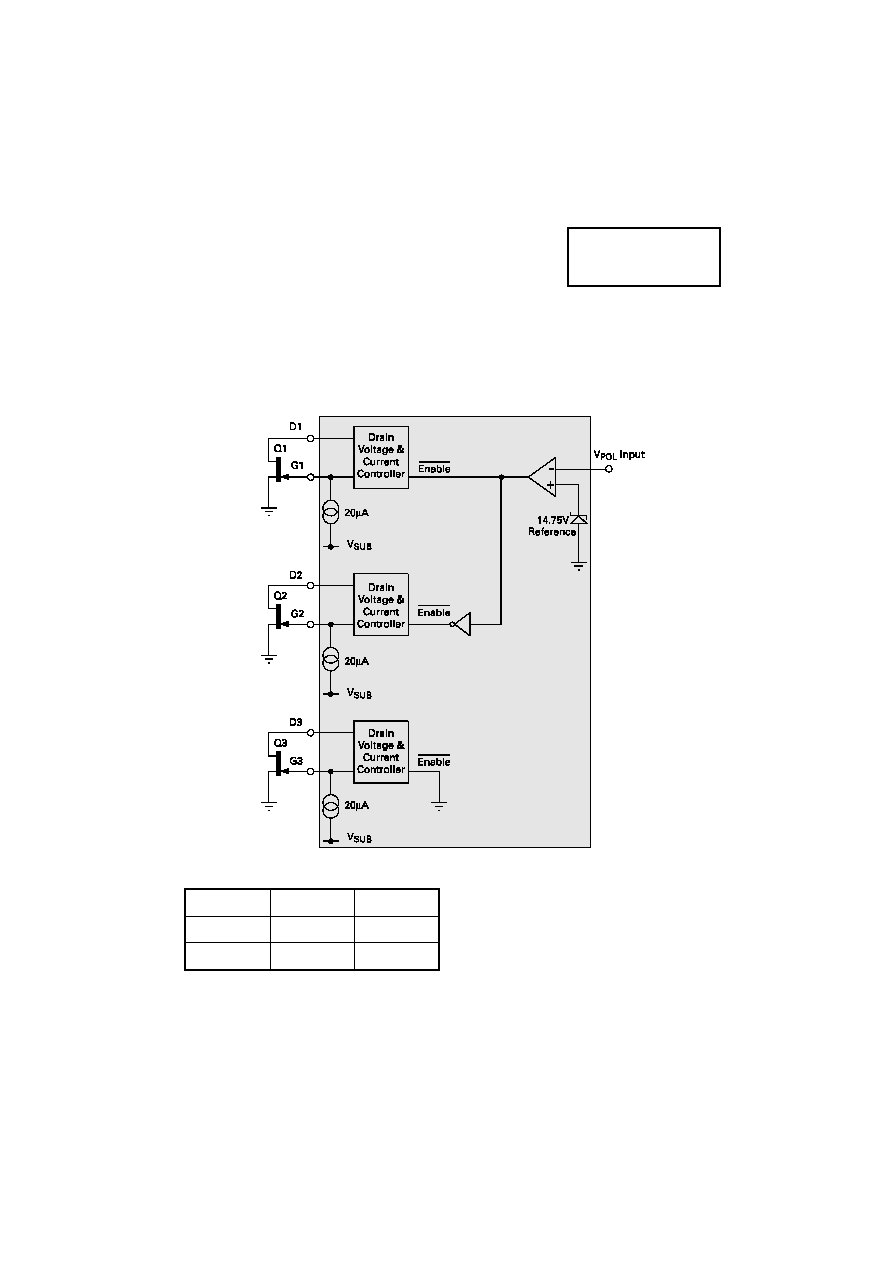
The following schematic shows the function of the V
POL
input. Only one of the two external FETs
numberd Q1 and Q2 are powered at any one time, their selection is controlled by the input V
POL
.
This input is designed to be wired to the power input of the LNB via a high value (10k) resistor.
With the input voltage of the LNB set at or below 14V, FET Q2 will be enabled. With the input
voltage at or above 15.5V, FET Q1 will be enabled. The disabled FET has its gate driven low and
its drain terminal is switched open circuit. It is permissible to connect the drain pins D1 and D2
together if required by the application circuit. FET number Q3 is always active regardless of the
voltage applied to V
POL
.
Control Input Switch Function
Input Sense
Polarisation
Select
14 volts
Vertical
FET Q2
15.5 volts
Horizontal
FET Q1
4-131
ZNBG3113
ZNBG3114
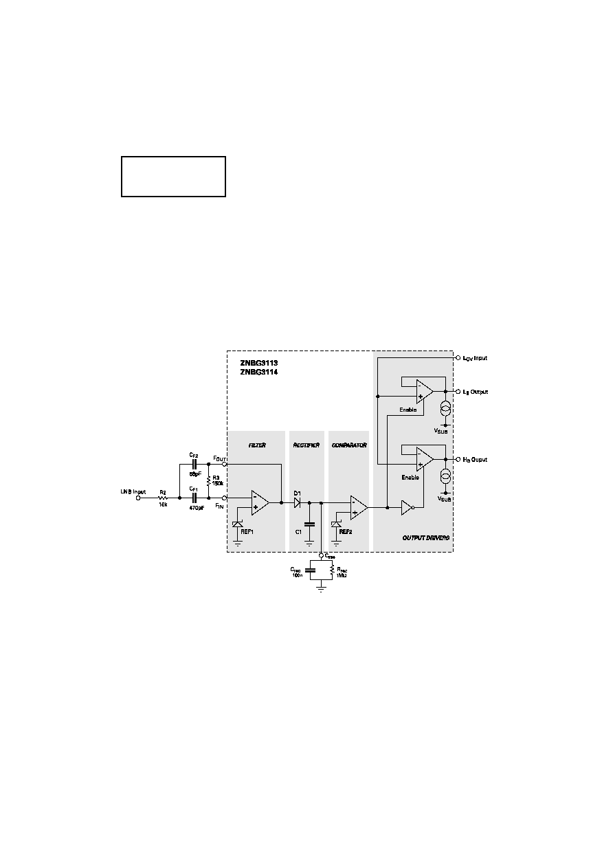
For many LNB applications tone detection and band switching is required. The ZNBG3113/14
includes the circuitry necessary to detect the presence of a 22kHz tone modulated on the supply
input to the LNB. Referring to the following schematic diagram, the main elements of this detector
are an op-amp enabling the construction of a Sallen Key filter, a rectifier/smoother and a
comparator. Full control is given over the centre frequency and bandwidth of the filter by the
selection of two external resistors and capacitors (one of these resistors, R2, shares the function
of overvoltage protection of pin V
POL
).
Pin C
rec
makes accessible the output of the tone switch rectifier and provides a means of
controlling tone switch delays (mainly HB-LB). For correct operation of the IC, a capacitor and a
parallel connected resistor should be connected between this pin and ground. A capacitor of
100nF and resistor of 1MW will give a LB-HB delay of around 100
µ
s and a HB-LB delay of 30ms.
The comparator circuit utilises no external components.
4-132
ZNBG3113
ZNBG3114
4-133
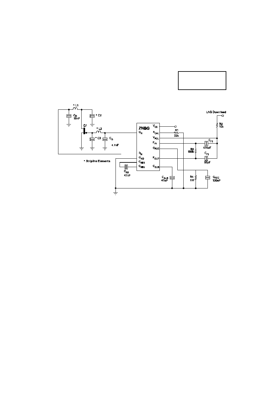
APPLICATIONS CIRCUIT
APPLICATIONS INFORMATION
The above is a partial application circuit for the ZNBG series showing all external components
required for appropriate biasing. The bias circuits are unconditionally stable over the full
temperature range with the associated FETs and gate and drain capacitors in circuit.
Capacitors C
D
and C
G
ensure that residual power supply and substrate generator noise is not
allowed to affect other external circuits which may be sensitive to RF interference. They also
serve to suppress any potential RF feedthrough between stages via the ZNBG device. These
capacitors are required for all stages used. Values of 10nF and 4.7nF respectively are
recommended however this is design dependent and any value between 1nF and 100nF could
be used.
The capacitors C
NB
and C
SUB
are an integral part of the ZNBGs negative supply generator. The
negative bias voltage is generated on-chip using an internal oscillator. The required value of
capacitors C
NB
and C
SUB
is 47nF. This generator produces a low current supply of approximately
-3 volts. Although this generator is intended purely to bias the external FETs, it can be used to
power other external circuits via the C
SUB
pin.
Resistor R
CAL
sets the drain current at which all external FETs are operated. If any bias control
circuit is not required, its related drain and gate connections may be left open circuit without
affecting the operation of the remaining bias circuits.
The ZNBG devices have been designed to protect the external FETs from adverse operating
conditions. With a JFET connected to any bias circuit, the gate output voltage of the bias circuit
can not exceed the range -3.5V to 1V under any conditions, including powerup and powerdown
transients. Should the negative bias generator be shorted or overloaded so that the drain current
of the external FETs can no longer be controlled, the drain supply to FETs is shut down to avoid
damage to the FETs by excessive drain current.
ZNBG3113
ZNBG3114
ZNBG3113
ZNBG3114
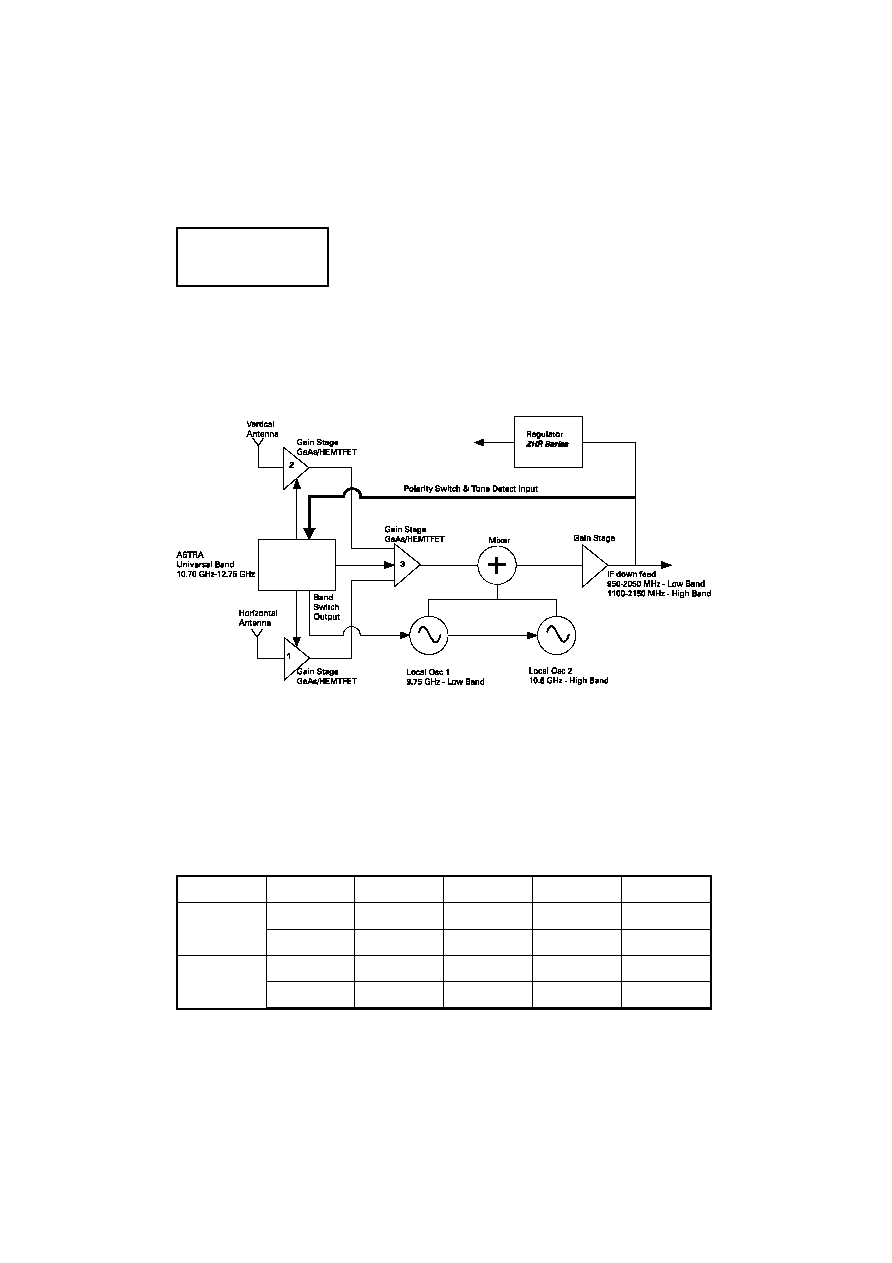
Single Universal LNB Block Diagram
The following block diagram shows the main section of an LNB designed for use with the Astra
series of satellites. The ZNBG3113/14 is the core bias and control element of this circuit. The
ZNBG provides the negative rail, FET bias control, polarisation switch control, tone detection and
band switching with the minimum of external components. Compared to other discrete
component solutions the ZNBG circuit reduces component count and overall size required.
APPLICATIONS INFORMATION(cont)
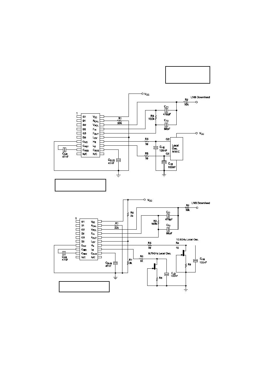
Tone detection and band switching is provided on the ZNBG3113/14 devices. The following
diagrams describes how this feature operates in an LNB and the external components required.
The presence or absence of a 22kHz tone applied to pin F
IN
enables one of two outputs, L
B
and
H
B
. A tone present enables H
B
and tone absent enables L
B
. The L
B
and H
B
outputs are designed
to be compatible with both MMIC and discrete local oscillator applications, selected by pin L
OV
.
Referring to Figure 1 wiring pin L
OV
to ground will force L
B
and H
B
to switch between -2.6V
(disabled) and 0V (enabled). Referring to Figure 2 wiring pin L
OV
to a positive voltage source (e.g.
a potential divider across V
CC
and ground set to the required oscillator supply voltage, V
OSC
) will
force the L
B
and H
B
outputs to provide the required oscillator supply, V
OSC
, when enabled.
Tone Detection Function
L
OV
F
IN
L
B
H
B
L
B
H
B
G
ND
22kHz
Disabled
Enabled
-2.6 volts
G
ND
--
Enabled
Disabled
G
ND
-2.6 volts
V
OSC
22kHz
Disabled
Enabled
Note 1
V
OSC
--
Enabled
Disabled
V
OSC
Note 1
Note 1: 0 volts in typical LNB applications but ependent on extenal circuits.
4-134
ZNBG3113
ZNBG3114
4-135
Figure 1
L
OV
grounded
Figure
2
L
OV
connected to V
OSC

4-136
ZNBG3113
ZNBG3114
ORDERING INFORMATION
Part Number
Package
Part Mark
ZNBG3113Q20
QSOP20
ZNBG3113
ZNBG3114Q20
QSOP20
ZNBG3114
CONNECTION DIAGRAM
ZNBG3113
ZNBG3114
Page Number
PACKAGE DIMENSIONS
PIN No.1
IDENTIFICATION
RECESS
FOR PIN 1
A
B
D
C
K
PIN
Millimetres
Inches
MIN
MAX
MIN
MAX
A
8.55
8.74
0.337
0.344
B
0.635
0.025 NOM
C
1.42
1.52
0.056
0.06
D
0.20
0.30
0.008
0.012
E
3.81
3.99
0.15
0.157
F
1.35
1.75
0.053
0.069
G
0.10
0.25
0.004
0.01
J
5.79
6.20
0.228
0.244
K
0∞
8∞
0∞
8∞
ZNBG3113
ZNBG3114
Zetex plc.
Fields New Road, Chadderton, Oldham, OL9-8NP, United Kingdom.
Telephone: (44)161 622 4422 (Sales), (44)161 622 4444 (General Enquiries)
Fax: (44)161 622 4420
Zetex GmbH
Zetex Inc.
Zetex (Asia) Ltd.
These are supported by
Streitfeldstraþe 19
47 Mall Drive, Unit 4
3510 Metroplaza, Tower 2
agents and distributors in
D-81673 M¸nchen
Commack NY 11725
Hing Fong Road,
major countries world-wide
Germany
USA
Kwai Fong, Hong Kong
©
Zetex plc 1998
Telefon: (49) 89 45 49 49 0
Telephone: (516) 543-7100
Telephone:(852) 26100 611
Fax: (49) 89 45 49 49 49
Fax: (516) 864-7630
Fax: (852) 24250 494
Internet:http://www.zetex.com
This publication is issued to provide outline information only which (unless agreed by the Company in writing) may not be used, applied
or reproduced for any purpose or form part of any order or contract or be regarded as a representation relating to the products or
services concerned. The Company reserves the right to alter without notice the specification, design, price or conditions of supply of
any product or service.
