DEVICE DESCRIPTION
The ZR404 uses a bandgap circuit design to
achieve a precision voltage reference of 2.45
volts. The device is available in small outline
s u r f a c e m o u n t p a c k a g e s , i d e a l fo r
a p p l i c a t i o n s w h e re s p a c e s a v i n g i s
important as well as a 2 pin TO92 style
package for through hole requirements.
The ZR404 design provides a stable voltage
without an external capacitor and is stable
wi th capaci tive loads. The ZR404 is
recommended for operation between 2mA
and 120mA.
FEATURES
∑
Small outline SO8 and TO92
style packages
∑
No stabilising capacitor required
∑
Typical T
C
15ppm/∞C
∑
Typical slope resistance 0.26
∑
±
3% tolerance
∑
Industrial temperature range (Military
temperature range available on request)
∑
Operating current 2mA to 120mA
∑
Alternative package options and
tolerances are available
APPLICATIONS
∑
Battery powered and portable
equipment.
∑
Metering and measurement systems.
∑
Instrumentation.
∑
Test equipment.
∑
Data acquisition systems.
∑
Precision power supplies.
PRECISION 2.45 VOLT
VOLTAGE REFERENCE
ISSUE 2 -- FEBRUARY 1998
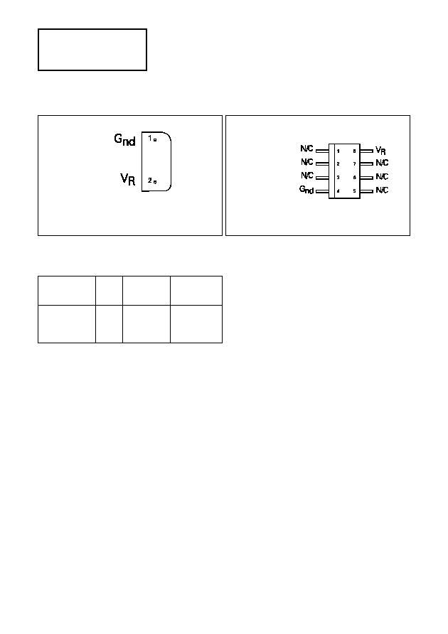
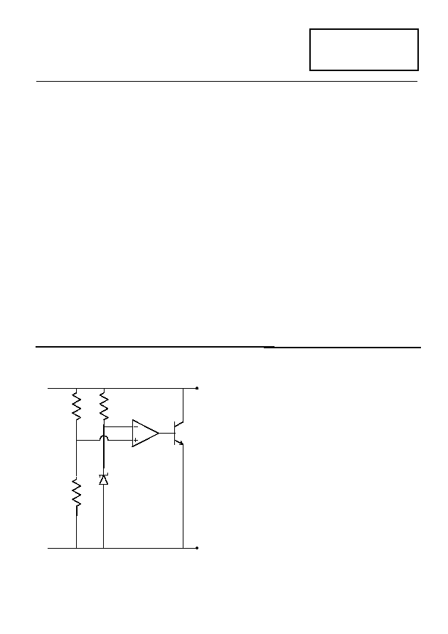
ZR404
V
R
G
nd
1.25V
REF
SCHEMATIC DIAGRAM
4-169

ABSOLUTE MAXIMUM RATING
Reverse Current
200mA
Forward Current
25mA
Operating Temperature
-40 to 85∞C
Storage Temperature
-55 to 125∞C
Power Dissipation (T
amb
=25∞C)
E-Line, 2 pin (TO92)
500mW
SO8
625mW
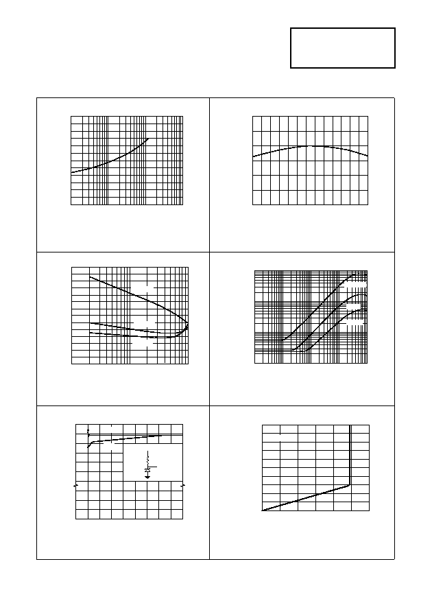
ELECTRICAL CHARACTERISTICS
TEST CONDITIONS (Unless otherwise stated) T
amb
=25∞C
SYMBOL PARAMETER
CONDITIONS
LIMITS
TOL.
%
UNITS
MIN
TYP MAX
V
R
Reverse Breakdown Voltage
I
R
=5mA
2.38
2.45 2.52
3
V
I
MIN
Minimum Operating Current
2
mA
I
R
Recommended Operating
Current
2
120
mA
T
C
Average Reverse Breakdown
Voltage Temp. Co.
I
R(min)
to
I
R(max)
15
50
ppm/∞C
R
S
ß
Slope Resistance
0.26 0.5
Z
R
Reverse Dynamic Impedance
I
R
= 5mA
f = 100Hz
I
AC
= 0.1 I
R
0.28 1
E
N
Wideband Noise Voltage
I
R
= 5mA
f = 10Hz to
10kHz
65
µ
V(rms)
ZR404
T
C
=
(
V
R
(
max
)
-
V
R
(
min
)
)
x 1000000
V
R
x
(
T
(
max
)
-
T
(
min
)
)
Note: V
R(max)
- V
R(min)
is the maximum
deviation in reference voltage measured
over the full operating temperature
range.
ß R
S
=
V
R
Change
(
I
R
(
min
)
to I
R
(
max
))
I
R
(
max
)
-
I
R
(
min
)
4-170