 | –≠–ª–µ–∫—Ç—Ä–æ–Ω–Ω—ã–π –∫–æ–º–ø–æ–Ω–µ–Ω—Ç: ZR78L10N8 | –°–∫–∞—á–∞—Ç—å:  PDF PDF  ZIP ZIP |
2.85 TO 12 VOLT FIXED POSITIVE
LOCAL VOLTAGE REGULATOR
ISSUE 3 - DECEMBER 2001
DEVICE DESCRIPTION
The ZR78L Series three terminal fixed positive
voltage regulators feature internal circuit
current limit and thermal shutdown making
the devices difficult to destroy. The circuit
design allows creation of any custom voltage
in the range 2.85 to 12 volts. The devices are
available in a small outline surface mount
package, ideal for applications where space
saving is important, as well as through hole
TO92 style packaging. The devices are suited
to local voltage regulation applications, where
problems could be encountered with
distributed single source regulation, as well as
more general voltage regulation applications.
The ZR78L Series show performance
characteristics superior to other local voltage
regulators. The initial output voltage is
maintained to within 2.5% with a quiescent
current of typically 350
µ
A. Output voltage
change, with input voltage and load current, is
much lower than competitive devices. The
ZR78L devices are completely stable with no
external components. The device will shut
down under thermal overload conditions but
as the device cools, regulation will restart.
FEATURES
∑
Small outline SOT223 package
∑
SO8 package (3.3V and 5.0V)
∑
TO92 package
∑
2.85 to 12 Volt
∑
Output current up to 200mA
∑
Tight initial tolerance
∑
Low quiescent current
∑
-55 to 125∞C temperature range
∑
No external components
∑
Internal thermal shutdown
∑
Internal short circuit current limit
VOLTAGE RANGE
ZR78L028
2.85V
ZR78L03
3.0V
ZR78L033
3.3V
ZR78L04
4.0V
ZR78L048
4.85V
ZR78L05
5.0V
ZR78L052
5.2V
ZR78L057
5.7V
ZR78L06
6.0V
ZR78L07
7.0V
ZR78L08
8.0V
ZR78L085
8.5V
ZR78L09
9.0V
ZR78L10
10.0V
ZR78L12
12.0V
ZR78L
SERIES
4-200

ZR78L
SERIES
ZR78L028 TEST CONDITIONS (Unless otherwise stated):T
j
=25∞C, I
O
=100mA, V
in
=6.85V
SYMBOL
PARAMETER
CONDITIONS
MIN.
TYP.
MAX.
UNITS
V
O
Output Voltage
2.78
2.85
2.92
V
I
O
=1 to 200mA
2.736
2.964
V
V
in
=4.85 to 20V
I
O
=1 to 100mA
2.736
2.964
V
V
O
Line Regulation
V
in
=4.85 to 20V
10
40
mV
V
O
Load Regulation
I
O
=1 to 200mA
I
O
=1 to 100mA
5
2
25
mV
mV
l
q
Quiescent Current
350
600
µ
A
l
q
Quiescent Current Change I
O
=1 to 200mA
V
in
=4.85 to 20V
100
100
µ
A
µ
A
V
n
Output Noise Voltage
f=10Hz to 10kHz
75
µ
V rms
V
in
/
V
O
Ripple Rejection
V
in
=5.85 to 18V
f=120Hz
48
62
dB
V
in
Input Voltage Required To
Maintain Regulation
4.85
4.55
V
V
O
/
T
Average Temperature
Coefficient of V
O
I
O
=5.0mA
0.1
mV/∞C
=T
j
=-55 to 125∞C
ELECTRICAL CHARACTERISTICS:
Notes:
1. The maximum operating input voltage and
output current of the device will be governed by
the maximum power dissipation of the selected
package. Maximum package power dissipation is
specified at 25 ∞C and must be linearly derated to
zero at T
amb
=125∞C.
2. The following data represents pulse test
conditions with junction temperatures as
indicated at the initiation of the test. Continuous
operation of the devices with the stated conditions
might exceed the power dissipation limits of the
chosen package.
3. Maximum power dissipation, for the SOT223
and SO8 packages, is calculated assuming that the
device is mounted on a PCB measuring 2 inches
square.
4. The shut down feature of the device operates if
its temperature exceeds its design limit as might
occur during external faults, short circuits etc. If the
regulator is supplied from an inductive source
then a large voltage transient, on the regulator
input, can result should the shut down circuit
operate. It is advised that a capacitor (1
µ
F or
greater) should be applied across the regulator
input to ensure that the maximum voltage rating
of the device is not exceeded under shutdown
conditions.
ABSOLUTE MAXIMUM RATING
Input voltage 20V
Output Current(I
o
) 200mA
Operating Temperature -55 to 125∞C
Storage Temperature -65 to 150∞C
Power Dissipation (T
amb
=25∞C)
SOT223 2W(Note 3)
TO92 600mW
S08 780mW(Note 3)
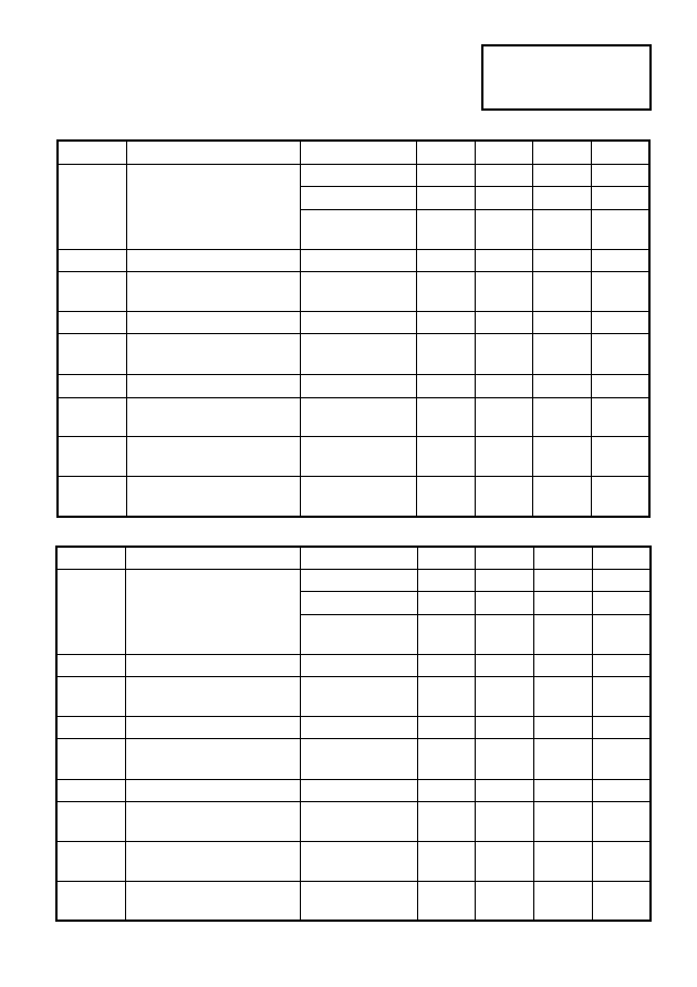
ZR78L03 TEST CONDITIONS (Unless otherwise stated):T
j
=25∞C, I
O
=100mA, V
in
=7V
SYMBOL
PARAMETER
CONDITIONS
MIN.
TYP.
MAX.
UNITS
V
O
Output Voltage
2.92
3.0
3.08
V
I
O
=1 to 200mA
2.88
3.12
V
V
in
=5 to 20V
I
O
=1 to 100mA
2.88
3.12
V
V
O
Line Regulation
V
in
=5 to 20V
10
40
mV
V
O
Load Regulation
I
O
=1 to 200mA
I
O
=1 to 100mA
5
2
25
mV
mV
l
q
Quiescent Current
350
600
µ
A
l
q
Quiescent Current Change
I
O
=1 to 200mA
V
in
=5 to 20V
100
100
µ
A
µ
A
V
n
Output Noise Voltage
f=10Hz to 10kHz
75
µ
V rms
V
in
/
V
O
Ripple Rejection
V
in
=6 to 18V
f=120Hz
48
62
dB
V
in
Input Voltage Required To
Maintain Regulation
5
4.7
V
V
O
/
T
Average Temperature
Coefficient of V
O
I
O
=5.0mA
0.1
mV/∞C
ZR78L033 TEST CONDITIONS (Unless otherwise stated):T
j
=25∞C, I
O
=100mA, V
in
=7.3V
SYMBOL
PARAMETER
CONDITIONS
MIN.
TYP.
MAX.
UNITS
V
O
Output Voltage
3.218
3.3
3.382
V
I
O
=1 to 200mA
3.168
3.432
V
V
in
=5.3 to 20V
I
O
=1 to 100mA
3.168
3.432
V
V
O
Line Regulation
V
in
=5.3 to 20V
7.5
30
mV
V
O
Load Regulation
I
O
=1 to 200mA
I
O
=1 to 100mA
5
2
25
mV
mV
l
q
Quiescent Current
350
600
µ
A
l
q
Quiescent Current Change
I
O
=1 to 200mA
V
in
=5.3 to 20V
100
100
µ
A
µ
A
V
n
Output Noise Voltage
f=10Hz to 10kHz
50
µ
V rms
V
in
/
V
O
Ripple Rejection
V
in
=6.3 to 18V
f=120Hz
50
64
dB
V
in
Input Voltage Required To
Maintain Regulation
5.3
5
V
V
O
/
T
Average Temperature
Coefficient of V
O
I
O
=5.0mA
0.1
mV/∞C
=T
j
= -55 to 125 ∞C
ZR78L
SERIES
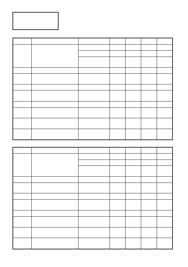
ZR78L04 TEST CONDITIONS (Unless otherwise stated):T
j
=25∞C, I
O
=100mA, V
in
=8V
SYMBOL
PARAMETER
CONDITIONS
MIN.
TYP.
MAX.
UNITS
V
O
Output Voltage
3.9
4.0
4.1
V
I
O
=1 to 200mA
3.84
4.16
V
V
in
=6 to 20V
I
O
=1 to 100mA
3.84
4.16
V
V
O
Line Regulation
V
in
=6 to 20V
10
40
mV
V
O
Load Regulation
I
O
=1 to 200mA
I
O
=1 to 100mA
5
2
25
mV
mV
l
q
Quiescent Current
350
600
µ
A
l
q
Quiescent Current Change
I
O
=1 to 200mA
V
in
=6 to 20V
100
100
µ
A
µ
A
V
n
Output Noise Voltage
f=10Hz to 10kHz
75
µ
V rms
V
in
/
V
O
Ripple Rejection
V
in
=7 to 18V
f=120Hz
48
62
dB
V
in
Input Voltage Required To
Maintain Regulation
6
5.3
V
V
O
/
T
Average Temperature
Coefficient of V
O
I
O
=5.0mA
0.1
mV/∞C
ZR78L
SERIES
ZR78L048 TEST CONDITIONS (Unless otherwise stated):T
j
=25∞C, I
O
=100mA, V
in
=8.85V
SYMBOL
PARAMETER
CONDITIONS
MIN.
TYP.
MAX.
UNITS
V
O
Output Voltage
4.729
4.85
4.971
V
I
O
=1 to 200mA
4.656
5.044
V
V
in
=6.8 to 20V
I
O
=1 to 100mA
4.656
5.044
V
V
O
Line Regulation
V
in
=6.85 to 20V
10
40
mV
V
O
Load Regulation
I
O
=1 to 200mA
I
O
=1 to 100mA
5
2
25
mV
mV
l
q
Quiescent Current
350
600
µ
A
l
q
Quiescent Current Change
I
O
=1 to 200mA
V
in
=6.85 to 20V
100
100
µ
A
µ
A
V
n
Output Noise Voltage
f=10Hz to 10kHz
50
µ
V rms
V
in
/
V
O
Ripple Rejection
V
in
=7.85 to 18V
f=120Hz
50
64
dB
V
in
Input Voltage Required To
Maintain Regulation
6.85
6.55
V
V
O
/
T
Average Temperature
Coefficient of V
O
I
O
=5.0mA
0.1
mV/∞C
=T
j
= -55 to 125∞C
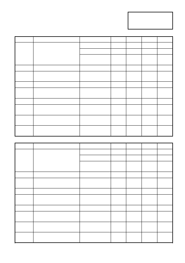
ZR78L12TEST CONDITIONS (Unless otherwise stated):T
j
=25∞C, I
O
=100mA, V
in
=16V
SYMBOL
PARAMETER
CONDITIONS
MIN.
TYP.
MAX.
UNITS
V
O
Output Voltage
11.7
12
12.3
V
I
O
=1 to 200mA
11.52
12.48
V
V
in
=14 to 20V
I
O
=1 to 100mA
11.52
12.48
V
V
O
Line Regulation
V
in
=14 to 20V
12
40
mV
V
O
Load Regulation
I
O
=1 to 200mA
I
O
=1 to 100mA
9
3
30
mV
mV
l
q
Quiescent Current
350
600
µ
A
l
q
Quiescent Current Change
I
O
=1 to 200mA
V
in
=14 to 20V
100
100
µ
A
µ
A
V
n
Output Noise Voltage
f=10Hz to 10kHz
150
µ
V rms
V
in
/
V
O
Ripple Rejection
V
in
=15 to 18V
f=120Hz
43
57
dB
V
in
Input Voltage Required To
Maintain Regulation
14
13.7
V
V
O
/
T
Average Temperature
Coefficient of V
O
I
O
=5.0mA
0.25
mV/∞C
=T
j
= -55 to 125 ∞C
ZR78L
SERIES
ZR78L10TEST CONDITIONS (Unless otherwise stated):T
j
=25∞C, I
O
=100mA, V
in
=14V
SYMBOL
PARAMETER
CONDITIONS
MIN.
TYP.
MAX.
UNITS
V
O
Output Voltage
9.75
10
10.25
V
I
O
=1 to 200mA
9.6
10.4
V
V
in
=12 to 20V
I
O
=1 to 100mA
9.6
10.4
V
V
O
Line Regulation
V
in
=12 to 20V
12
40
mV
V
O
Load Regulation
I
O
=1 to 200mA
I
O
=1 to 100mA
9
3
30
mV
mV
l
q
Quiescent Current
350
600
µ
A
l
q
Quiescent Current Change
I
O
=1 to 200mA
V
in
=12 to 20V
100
100
µ
A
µ
A
V
n
Output Noise Voltage
f=10Hz to 10kHz
150
µ
V rms
V
in
/
V
O
Ripple Rejection
V
in
=13 to 18V
f=120Hz
43
57
dB
V
in
Input Voltage Required To
Maintain Regulation
12
11.7
V
V
O
/
T
Average Temperature
Coefficient of V
O
I
O
=5.0mA
0.25
mV/∞C