 | –≠–ª–µ–∫—Ç—Ä–æ–Ω–Ω—ã–π –∫–æ–º–ø–æ–Ω–µ–Ω—Ç: ZRT100GC1 | –°–∫–∞—á–∞—Ç—å:  PDF PDF  ZIP ZIP |
9.8V LOW POWER
PRECISION REFERENCE SOURCE
ISSUE 1 - OCTOBER 1995
ZRT100
DEVICE DESCRIPTION
The ZRT100 is a monolithic integrated circuit
providing a precise stable reference voltage
of 9.8V at 500
µ
A.
The circuit features a knee current of 150
µ
A
and ope ra tion over a wide range of
temperatures and currents.
The ZRT100 is available in a 3-pin metal can
package for through hole applications as
well as SOT223 and SO8 packages for
surface mount applications. Each package
option offers a trim facility whereby the
output voltage can be adjusted as shown in
F i g . 1 . T h i s f a c i l i t y i s u s e d w h e n
compensating for system errors or setting
the reference output to a particular value.
When the trim facility is not used, the pin
should be left open circuit.
FEATURES
∑
Trimmable output
∑
Excellent temperature stability
∑
Low output noise figure
∑
Available in two temperature ranges
∑
1 and 2% initial voltage tolerance
versions available
∑
No external stabilising capacitor
required in most cases
∑
Low slope resistance
∑
TO18 package
∑
SOT223 and SO8 small outline
packages
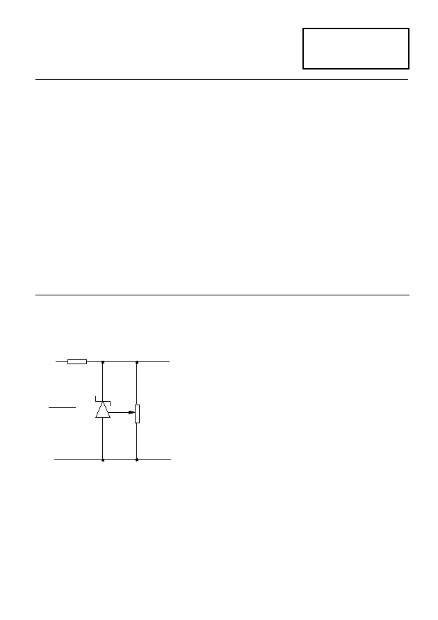
R
V
CC
V
R
G
nd
G
nd
R
T
=100k
(Optional trim facility)
R=V
CC
-V
R
I
R
Figure 1:
This circuit will allow the reference to be
trimmed over a wide range. The device is
specified over a 5% trim range
.
SCHEMATIC DIAGRAM
4-295

ABSOLUTE MAXIMUM RATING
Reverse Current
30mA ¯
Operating Temperature
A grade
-55∞C to 125∞C
C grade
0∞C to 70∞C
Storage Temperature
TO18
-55 ∞C to 175 ∞C
SO8, SOT223 -55 ∞C to 125 ∞C
Power Dissipation (T
amb
=25∞C)
TO18
300mW
SO8
625mW
SOT223
2W
¯ Above 25∞C this figure should be linearly
derated to 6mA at 125∞C
ELECTRICAL CHARACTERISTICS
( at T
amb
=25∞C and Trim pin o/c unless otherwise stated)
SYMBOL
PARAMETER
MIN.
TYP. MAX. UNITS
COMMENTS
V
R
Output voltage
1% tolerance (A1,C1)
2% tolerance (C2)
9.70
9.60
9.80
9.80
9.90
10.00
V
I
R
=500
µ
A
V
TRIM
Output voltage adjustment
range
5
%
R
T
=100k
T
C
V
TRIM
Change in TCV
R
with output
adjustment
5.0
ppm/∞C/%
I
R
Operating current range
0.15
30
mA
See note (c)
t
on
t
off
Turn-on time
Turn-off time
400
0.3
µ
s
R
L
=1k
e
np-p
Output voltage noise (over
the range 0.1 to 10Hz)
50
µ
V
Peak to peak
measurement
R
S
Slope resistance
1.8
4.0
I
R
=
0.5mA to 5mA
See note (d)
ZRT100
TEMPERATURE DEPENDENT ELECTRICAL CHARACTERISTICS
SYMBOL PARAMETER
INITIAL
VOLTAGE
TOLERANCE
%
GRADE A
-55∞C TO 125∞C
GRADE C
0∞C TO 70∞C
UNITS
TYP
MAX
TYP
MAX
V
R
Output voltage
change over relevant
temperature range
(See note (a))
1 & 2
27.0
90.0
10.8
34.4
mV
T
C
V
R
Output voltage
temperature
coefficient (See note
(b))
1 & 2
15.0
50.0
15.0
50.0
ppm/∞C
4-296
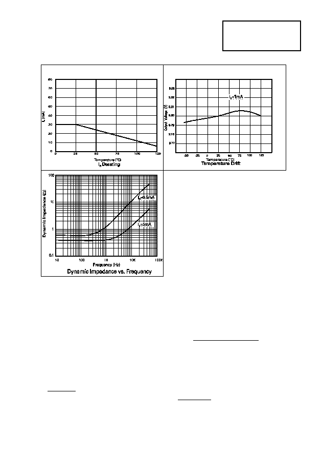
TYPICAL CHARACTERISTICS
ZRT100
NOTES
(a) Output change with temperature (V
R
)
The absolute maximum difference between
the maximum output voltage and the
minimum output voltage over the specified
temperature range
V
R
= V
max
- V
min
(b) Output temperature coefficient (T
C
V
R
)
The ratio of the output change with
temperature to the specified temperature
range expressed in ppm/∞C
T
c
V
R
=
V
R
x
10
6
V
R
x
T
ppm
/
∞
C
T= Full temperature range
(c) Operating current (I
R
)
Maximum operating current must be
derated as indicated in maximum ratings.
(d) Slope
resistance
(R
S
)
The slope resistance is defined as :
R
S
=
change
in
V
R
specifiedcurrentrange
I = 5 - 0.5 = 4.5mA (typically)
(e) Line
regulation
The ratio of change in output voltage to the
change in input voltage producing it.
R
S
x 100
V
R
x
R
source
%
/
V
4-297
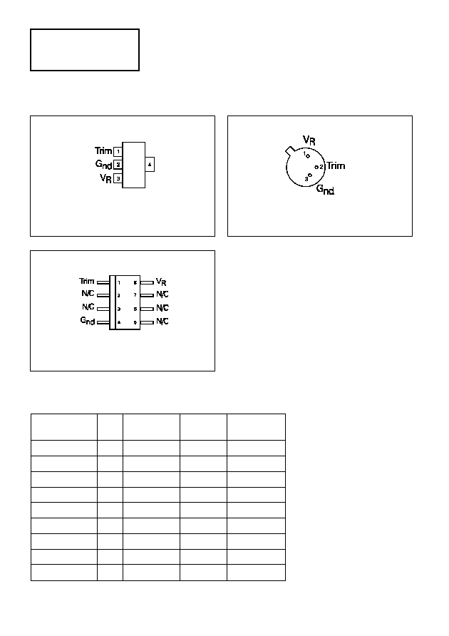
SO8 Package Suffix ≠ N8
Top
View
TO18 Package Suffix ≠ None
Bottom View ≠
Case
is
internally
connected
to
pin
3
SOT223
Package
Suffix ≠ G
Top
View
Pin 4 floating or connected to pin 2
CONNECTION DIAGRAMS
Part No
Tol% Operating
Temp.(∞C)
Package
Partmark
ZRT100C2
2
0 to 70
TO18
ZRT100C2
ZRT100C1
1
0 to 70
TO18
ZRT100C1
ZRT100A1
1
-55 to 125
TO18
ZRT100A1
ZRT100GC2
2
0 to 70
SOT223
ZRT100C2
ZRT100GC1
1
0 to 70
SOT223
ZRT100C1
ZRT100GA1
1
-55 to 125
SOT223
ZRT100A1
ZRT100N8C2
2
0 to 70
SO8
ZRT100C2
ZRT100N8C1
1
0 to 70
SO8
ZRT100C1
ZRT100N8A1
1
-55 to 125
SO8
ZRT100A1
ORDERING INFORMATION
ZRT100
4-298