 | –≠–ª–µ–∫—Ç—Ä–æ–Ω–Ω—ã–π –∫–æ–º–ø–æ–Ω–µ–Ω—Ç: ZSD100N8 | –°–∫–∞—á–∞—Ç—å:  PDF PDF  ZIP ZIP |
AUTOMOTIVE AND HOUSEHOLD
SECURITY SIREN DRIVER
ISSUE 6 ≠ JANUARY 1998
INTRODUCTION
The ZSD100 is a frequency swept alarm
signal generator designed specifically for
static and automotive security alarm
s y s t e m s . O n e Z S D 1 0 0 , t w o t i mi n g
capacitors, an in-expensive TO92 darlington,
piezo transducer and coupling transformer
is all that is necessary to produce an ear
piercing 120 dB alarm siren.
Includin g an au dio frequency signal
generator, low frequency sweep generator,
disable circuitry and output driver stages,
th e ZSD1 00 provid es e v ery function
necessary to produce a standard alarm
signal. Available in either an 8 pin DIL or SO
package the IC gives a low cost compact
solution to siren signal generation. The
device operates from supplies of 4V up to
18V and is ideal for security alarms in battery
powered applications, burglar alarms and
automotive anti theft systems.
FEATURES
∑
4-18V Operating voltage range.
∑
Small external component count.
∑
Direct drive of darlington, mosfet and
IGBT output stages.
∑
Single ended or push-pull output
stages.
∑
Suitable for automotive and static
alarm systems.
∑
Low supply current - 10mA operating
- 1
µ
A sleep mode
∑
Low cost 8 pin DIL & SO packages.
∑
User selected audio and sweep
frequencies.
∑
-40∞C to 125∞C operating temperature
range.
∑
Choice of modulation waveform.
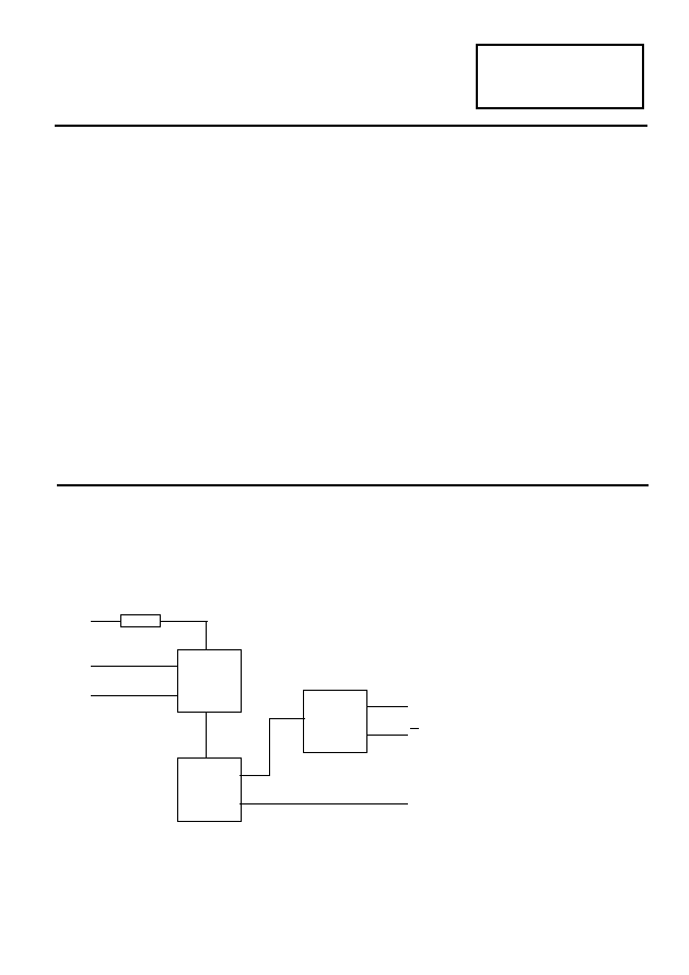
ZSD100
Low
Frequency
Oscillator
Output
Driver
Q
Oscillator
Output
Control
Voltage
Audio
Voltage
Controlled
Oscillator
SAW
C
R
R (INT)
Q
T
T
MOD
C
OUT
SCHEMATIC DIAGRAM
4-321
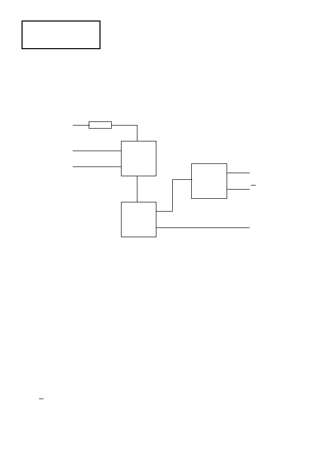
ZSD100
Low
Frequency
Oscillator
Output
Driver
Q
Oscillator
Output
Control
Voltage
Audio
Voltage
Controlled
Oscillator
SAW
C
R
R (INT)
Q
T
T
MOD
C
OUT
PIN DESCRIPTIONS
1.
R
T
Optional external resistor for improved frequency control. An external resistor
improves the control of both the modulating and output oscillators.
The R
T
pin is also used to power the device down. Either connecting R
T
to V
CC
or
an open circuit will result in the device being disabled.
2.
SAW
Selection of modulation waveform is made using the SAW pin. An open circuit
produces a triangle wave, sawtooth is achieved by connecting SAW to the C
MOD
pin.
3.
C
MOD
An external capacitor is used to program the low frequency modulating oscillator.
The value of C
MOD
recommended is between 0.1
µ
F and 10
0µ
F.
4.
G
ND
5.
C
OUT
An external capacitor is used to program the output oscillator. The value of C
OUT
recommended is between 1nF and 100nF.
6.
Q
Non inverted output driver
7.
Q
Inverted output driver
8.
V
CC
FUNCTIONAL DESCRIPTION
The audio signal of the ZSD100 is generated using a squarewave oscillator whose output is capable
of directly driving a wide range of output circuits. To produce a characteristic alarm siren sound, the
frequency of the audio oscillator is swept over a fixed 2:1 range by a second, low frequency oscillator.
The freqencies of both oscillators are controlled by R
T
(INT) and capacitors C
MOD
and C
OUT
.
4-322

ZSD100
ELECTRICAL CHARACTERISTICS
TEST CONDITIONS (Unless otherwise stated):T
amb
=25∞C, V
CC
=12V
PARAMETER
SYMBOL
MIN.
TYP.
MAX.
CONDITIONS.
Supply Voltage Operating
Range
V
CC
4V
18V
Supply Current
Disabled
Enabled
I
CC
1
µ
A
25mA
R
T
O/C, V
CC
=18V
R
T
, Q, Q at Gnd, V
CC
=18V
Modulating Oscillator
Frequency
Range
F
MOD
0.1Hz
10Hz
V
CC
=4 to 18V
Frequency
Value
See Note 1
F
MOD
3.3Hz
5.1Hz
4.3Hz
5.5Hz
5.4Hz
5.9Hz
R
T
=0, C
MOD
=10
µ
F
R
T
=470k
, C
MOD
=1
µ
F
Output Oscillator
Frequency
Range
Centre
Frequency
( Note 2)
Deviation
Duty Cycle
F
OUT
100Hz
10kHz
V
CC
=4 to 18V
F
OUT
F
OUT
1.01kHz
1.26kHz
±
33%
49%
1.58kHz
55%
R
T
=0, C
OUT
=22nF
Output
Source
Current
Sink
Current
Open Circuit Voltage
I
SOURCE
I
SINK
V
OUT(HIGH)
V
OUT(LOW)
5mA
0.5mA
V
CC
-1.5V
0.5V
V
OUT
=1.4V
V
OUT
=1.4V
I
OUT
=100
µ
A
I
SINK
=0.1
µ
A
Frequency Control
Components
Internal
Resistor
External
Resistor
Modulation
Capacitor
Output
Capacitor
R
T
(INT)
R
T
(EXT)
C
MOD
C
OUT
0
0.1
µ
F
1nF
61.5k
1M
100
µ
F
100nF
Note 1.
F
MOD
=
2850
C
MOD
(
61.5
+
R
T
(
EXT
)
)
Hz
C
MOD
in
µ
F, R
T
(EXT) in k
Note 2.
F
OUT
=
1710
C
OUT
(
61.5
+
R
T
(
EXT
)
)
Hz
C
OUT
in
µ
F, R
T
(EXT) in k
ABSOLUTE MAXIMUM RATING
V
cc
-0.5V to +20V
Operating Temperature
-40 to 125∞C
Storage Temperature
-65 to 150∞C
Power Dissipation (T
amb
=25∞C)
SO8
625mW
DIL8
625mW
4-323

ZSD100
F
MO
D
-
M
odulation
Fre
quen
cy (Hz
)
F
MO
D
-
Norma
lised
M
o
dulation Fre
q
u
e
n
c
y
0
2
4
6
8
10
20
16
12
8
4
0
V =12V
CC
Q
Q
V
OUT
- Output Voltage (V)
I
SINK
-
Output Sink C
u
r
r
e
n
t
(mA)
I
SINK
v
V
OUT
TYPICAL CHARACTERISTICS
0
2
4
6
8
10
10
8
6
4
2
0
12
Q or Q
V
OUT
- Output Voltage (V)
I
SOURCE
v
V
OUT
I
SOURCE
-
O
u
t
put Sou
r
c
e
Cu
r
r
e
n
t
(
m
A
)
0
4
8
12
16
20
1.2
1.0
0.8
0.6
0.4
0.2
R
T
=470k
R
T
=0
V
CC
- Supply Voltage (V)
F
MOD
vV
CC
0
4
8
12
16
20
1.2
1.0
0.8
0.6
0.4
0.2
F
O
at V
CC
=12V = 1.4kHz
R
T
=470k
R
T
=0
V
CC
- Supply Voltage (V)
F
O
vV
CC
F
O
-
N
o
r
m
alise
d Output F
req
uenc
y
C
OUT
- Output Oscillator Capacitance (nF)
F
OUT
vC
OUT
C
MOD
- Modulation Capacitance (
µ
F)
F
MOD
v C
MOD
F
OU
T
-
Output
Ce
nt
re
F
requ
e
n
c
y
(
k
H
z
)
1.0
10
100
10
1.0
0.1
1
10
100
10
1.0
0.1
R
T
=470k
R
T
=0
R
T
=470k
R
T
=0
V =12V
CC
4-324

-50
-25
0
25
50
75
100
125
800
700
600
500
400
300
200
100
0
T
AMB
- Ambient Temperature (∞C)
P
DI
S
-
M
a
x
i
m
u
m
Pow
er
Di
ss
i
pat
ion
(
m
W)
Derating Curve
R =0
T
R =470K
T
C
MOD
=10
µ
F
C
OUT
=22nF
Q,Q O/C
0
4
8
12
16
20
10
8
6
4
2
0
V
CC
- Supply Voltage (V)
I
Q
-
Q
uie
sc
e
n
t
Cur
r
ent (
m
A)
I
Q
v V
CC
TYPICAL CHARACTERISTICS
ZSD100
4-325
ZSD100
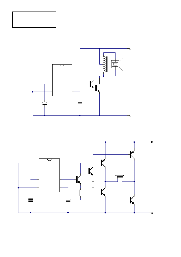
APPLICATIONS CIRCUITS
Piezo Sounder
Utilizing a standard autotransformer driven piezo sounder, this circuit indicates a minimum
component count alarm solution. In this configuration a ZTX605 darlington transistor can be
connected directly to the ouput of the IC without the need for base resistors.
Moving Coil Loudspeaker Sounder
Moving coil loudspeakers are often used for the very highest output automotive alarm sounders. The
ZSD100 complementary outputs, with the selection of ZTX790A and ZTX690B transistors, can drive
this H bridge ouput circuit without any additional interface components.
T
MOD
ND
CC
OUT
_
V
Q
Q
C
R
SAW
C
G
ZSD100
C
OUT
C
MOD
0V
+12V
ZTX
605
T1
Piezo
Sounder
T
MOD
ND
CC
OUT
_
V
Q
Q
C
R
SAW
C
G
ZSD100
C
OUT
C
MOD
MPS
2222
330
330
MPS
2222
ZTX
690B
ZTX
790A
ZTX
790A
ZTX
690B
SPEAKER
6
0V
+12V
4-326

ZSD100
Improved Frequency Control
Improved frequency control can be achieved with an external resistor between the R
T
pin and G
ND
.
An external resistor reduces the value of the timing capacitors required for the selected operating
frequency and also reduces the ZSD100's power consumption.
Note: The outputs of the ZSD100 have been designed to avoid cross-conduction in full bridge output
circuits. Large value external timing resistors can lead to a small level of cross-conduction. It is
recommended that external timing resistors are not used with bridge output circuits.
Remote Switching
If the R
T
pin is switched open-circuit, all internal functions of the IC are shut down.
Note: A small leakage current in the open collector logic controller will enable the IC. If such leakage
cannot be eliminated, its effect can be easily negated by adding a high value resistor (eg. 100k)
between pin R
T
and V
CC
. This resistor will have no effect on frequency control.
T
MOD
ND
CC
OUT
_
V
Q
Q
C
R
SAW
C
G
ZSD100
C
OUT
C
MOD
T
R
G
V
ND
CC
T
MOD
ND
CC
OUT
_
V
Q
Q
C
R
SAW
C
G
ZSD100
C
MOD
LOGIC
Open
collector
output
Logic supply
C
OUT
G
ND
V
CC
4-327
ZSD100
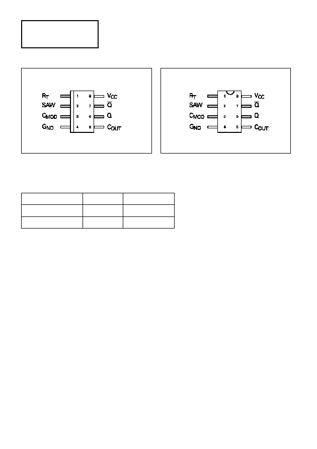
SO8 Package
Suffix ≠ N8
Top
View
DIL8 Package
Suffix ≠ D8
Top
View
CONNECTION DIAGRAMS
ORDERING INFORMATION
Part Number
Package
Part Mark
ZSD100D8
DIL8
ZSD100
ZSD100N8
SO8
ZSD100
4-328