 | –≠–ª–µ–∫—Ç—Ä–æ–Ω–Ω—ã–π –∫–æ–º–ø–æ–Ω–µ–Ω—Ç: ZSH330N8 | –°–∫–∞—á–∞—Ç—å:  PDF PDF  ZIP ZIP |
SUPPLY VOLTAGE
MONITOR
ISSUE 1 - DECEMBER 1997
ZSH330
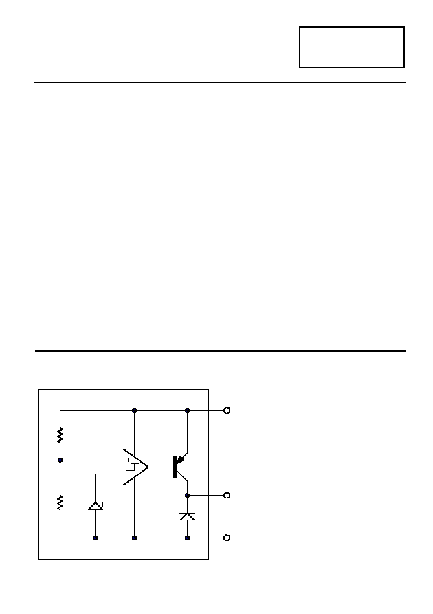
DEVICE DESCRIPTION
The ZSH330 is a three terminal under voltage
monitor circuit for use in microprocessor
systems. The threshold voltage of the device
has been set to 3.1 volts making it ideal for
3.3 volt circuits.
Included in the device is a precise voltage
reference and a comparator with built in
hysteresis to prevent erratic operation. The
ZSH330 features an open collector output
capable of sourcing at least l0mA which only
requires a single external resistor to
interface to following circuits.
Operation of the device is guaranteed from
one volt upwards, from this level to the
device threshold voltage the output is held
high providing a power on reset function.
Should the supply voltage, once established,
at any time drop below the threshold level
then the output again will pull high.
The device is available in a TO92 package for
through hole applications as well as SO8 and
SOT223 for surface mount requirements.
FEATURES
∑
SO8, SOT223 and TO92 packages
∑
Power on reset generator
∑
Automatic reset generation
∑
Low standby current
∑
Guaranteed operation from 1 volt
∑
Wide supply voltage range
∑
Internal clamp diode to discharge
delay capacitor
∑
3.1 volt threshold for 3.3 volt logic
∑
20mV hysteresis prevents erratic operation
APPLICATIONS
∑
Microprocessor systems
∑
Computers
∑
Computer peripherals
∑
Instrumentation
∑
Automotive
∑
Battery powered equipment
Vcc
Out
Gnd
SCHEMATIC DIAGRAM
4-329
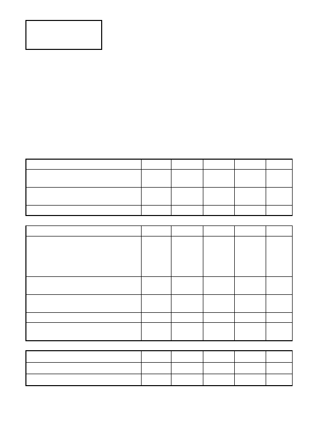
TEST CONDITIONS
(T
amb
=25∞C for typical values, T
amb
=-40 to 85∞C for min/max values (Note3))
COMPARATOR
PARAMETER
SYMBOL
MIN
TYP.
MAX.
UNITS
Threshold Voltage
Low state output (V
cc
increasing)
V
IL
3.01
3.09
3.15
V
Threshold Voltage
High state output (V
cc
decreasing)
V
IH
3.01
3.07
3.15
V
Hysteresis
V
H
0.01
0.02
0.05
V
OUPUT
PARAMETER
SYMBOL
MIN
TYP.
MAX.
UNITS
Output source saturation:
V
OH
(V
cc
=2.7V, I
source
=8.0mA)
V
CC
-1.3
V
(V
cc
=2.7V, I
source
=2.0mA)
V
CC
-1.2
V
(V
cc
=1.0V, I
source
=2
µ
A)
V
CC
-0.4
V
Onstate output source current
(V
cc
=2.7V, Output=0V)
I
source
10
21
50
mA
Offstate output leakage current
(V
cc
=3.3V, Output=0V)
I
oh
0.02
0.5
µ
A
Clamp diode forward voltage (I
f
=10mA)
V
f
0.6
1.2
1.5
V
Propagation delay
(V
in
3.3V to 2.7V, R
l
=10k, T
amb
=25∞C)
T
d
1.4
µ
s
TOTAL DEVICE
PARAMETER
SYMBOL
MIN
TYP.
MAX.
UNITS
Operating input voltage range
V
cc
1.0 to 6.5
V
Quiescent input current (V
cc
=3.3V)
I
q
130
180
µ
A
Note:
1. Maximum package power dissipation must be observed.
2. Maximum power dissipation, for the SOT223 and SO8 packages, is calculated assuming
that the device is mounted on a PCB measuring 2 inches square.
3. Low duty cycle pulse techniques are used during test to maintain junction temperatures as
close to ambient as possible.
ZSH330
ABSOLUTE MAXIMUM RATING
Input Supply Voltage
-1 to 10V
Offstate Output Voltage
10V
Onstate Output
Source Current(
Note 1
)
Internally limited
Clamp Diode
Forward Current(
Note 1
)
100mA
Operating Junction
Temperature
150∞C
Operating Temperature
-40 to 85∞C
Storage Temperature
-55 to 150∞C
Power Dissipation
TO92
780mW
SOT223
2W(
Note 2
)
SO8
780mW(
Note 2
)
4-330
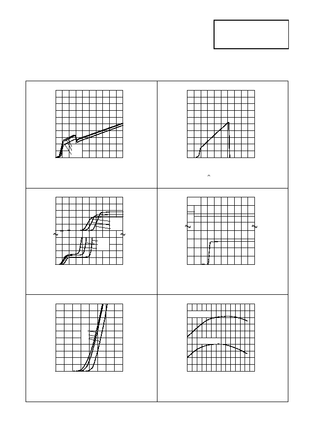
ZSH330
85∞C
25∞C
-40∞C
0
2
4
6
8
10
500
400
300
200
100
0
Input Voltage (V)
Input C
urre
nt (
µ
A)
Input Current v Input Voltage
5.0
4.0
3.0
2.0
1.0
0.0
0.0
1.0
2.0
3.0
4.0
5.0
Output V
o
l
t
a
ge
(V)
Input Voltage (V)
Output Voltage v Input Voltage
2.0
1.6
1.2
0.8
0.4
0.0
Output Saturation Voltage (V)
30
20
10
0
0.8
0.6
0.4
0.2
0.0
S
ource
Cu
r
r
e
n
t
(mA)
Output Saturation Voltage v
Source Current
85∞C
25∞C
-40∞C
85∞C
25∞C
-40∞C
3.3
2.7
2.0
4.0
2.0
0.0
Rl=10k
Vi
n(V)
V
out(V)
0
1
2
3
4
Time (
µ
s)
Reset Delay Time
0.0
0.4
0.8
1.2
1.6
Forward Voltage (V)
100
80
60
40
20
0
F
orwa
rd Curr
ent
(mA
)
Clamp Diode Forward Current v Voltage
85∞C
25∞C
-40∞C
-40 -20
0
20
40
60
80
100
Temperature (∞C)
3.10
3.09
3.08
3.07
3.06
3.05
T
h
r
e
shol
d V
o
l
t
a
ge
(V)
Threshold Voltage v Temperature
Upper
Threshold
Lower
Threshold
TYPICAL CHARACTERISTICS
4-331

ZSH330
Note 4: A time delayed reset can be accomplished with
the additional Cd.
T
DY
=
RCd
ln
1
V
TH
V
in
-
ln
1
1
-
V
SAT
V
in
TIMING DIAGRAM
APPLICATION CIRCUIT
T
DY
=Time (Seconds)
V
TH
=Microprocessor Reset Threshold
(ground referenced)
V
SAT
=Output Saturation Voltage ( from
Output Saturation Voltage characteristic)
V
in
=Power
Supply
Voltage
4-332

SO8 Package Suffix ≠ N8
Top
View
TO92 Package
Suffix ≠ C
Bottom
View
SOT223 Package Suffix ≠ G
Top View ≠
Connect pin 4 to pin 2 or leave pin 4
electrically isolated
CONNECTION DIAGRAMS
Part No
Package
Partmark
ZSH330C
TO92
ZSH330
ZSH330G
SOT223
ZSH330
ZSH330N8
SO8
ZSH330
ORDERING INFORMATION
ZSH330
4-333