P-CHANNEL ENHANCEMENT
MODE VERTICAL DMOS FET
ISSUE 2 SEPTEMBER 94
FEATURES
* 240 Volt V
DS
* R
DS(on)
=9
* Low threshold
APPLICATIONS
* Electronic Hook Switch
REFER TO ZVP4424A FOR GRAPHS
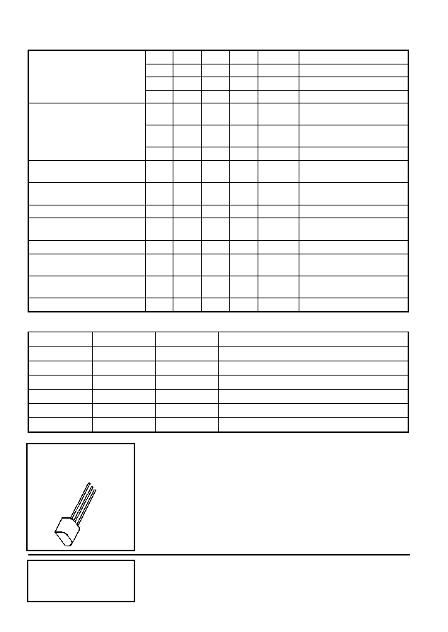
ABSOLUTE MAXIMUM RATINGS.
PARAMETER
SYMBOL
VALUE
UNIT
Drain-Source Voltage
V
DS
-240
V
Continuous Drain Current at T
amb
=25∞C
I
D
-200
mA
Pulsed Drain Current
I
DM
-1
A
Gate Source Voltage
V
GS
±
40
V
Power Dissipation at T
amb
=25∞C
P
tot
750
mW
Operating and Storage Temperature Range
T
j
:T
stg
-55 to +150
∞C
ELECTRICAL CHARACTERISTICS (at T
amb
= 25∞C unless otherwise stated).
PARAMETER
SYMBOL MIN. TYP
MAX. UNIT CONDITIONS.
Drain-Source Breakdown
Voltage
BV
DSS
-240
V
I
D
=-1mA, V
GS
=0V
Gate-Source Threshold
Voltage
V
GS(th)
-0.7
-1.4
-2.0
V
ID=-1mA, V
DS
= V
GS
Gate-Body Leakage
I
GSS
100
nA
V
GS
=
±
40V, V
DS
=0V
Zero Gate Voltage Drain
Current
I
DSS
-10
-100
µ
A
µ
A
V
DS
=-240 V, V
GS
=0
V
DS
=-190V, V
GS
=0V, T=125∞C
On-State Drain Current
I
D(on)
-0.75 -1.0
A
V
DS
=-10 V, V
GS
=-10V
Static Drain-Source
On-State Resistance
R
DS(on)
7.1
8.8
9
11
V
GS
=-10V,I
D
=-200mA
V
GS
=-3.5V,I
D
=-100mA
Forward
Transconductance (1) (2)
g
fs
125
mS
V
DS
=-10V,I
D
=-0.2A
Input Capacitance (2)
C
iss
100
200
pF
V
DS
=-25V, V
GS
=0V, f=1MHz
Common Source Output
Capacitance (2)
C
oss
18
25
pF
Reverse Transfer
Capacitance (2)
C
rss
5
15
pF
Turn-On Delay Time (2)(3)
t
d(on)
8
15
ns
V
DD
-
50V, I
D
=-0.25A,
V
GEN
=-10V
Rise Time (2)(3)
t
r
8
15
ns
Turn-Off Delay Time (2)(3)
t
d(off)
26
40
ns
Fall Time (2)(3)
t
f
20
30
ns
(1) Measured under pulsed conditions. Width=300
µ
s. Duty cycle
2% (2) Sample test.
(3) Switching times measured with 50
source impedance and <5ns rise time on a pulse generator
E-Line
TO92 Compatible
3-439
ZVP4424C
3-436
G
D
S
P-CHANNEL ENHANCEMENT
MODE VERTICAL DMOS FET
ISSUE 2 SEPTEMBER 94
FEATURES
* 240 Volt V
DS
* R
DS(on)
=9
* Low threshold
APPLICATIONS
* Electronic Hook Switch
ABSOLUTE MAXIMUM RATINGS.
PARAMETER
SYMBOL
VALUE
UNIT
Drain-Source Voltage
V
DS
-240
V
Continuous Drain Current at T
amb
=25∞C
I
D
-200
mA
Pulsed Drain Current
I
DM
-1
A
Gate Source Voltage
V
GS
±
40
V
Power Dissipation at T
amb
=25∞C
P
tot
750
mW
Operating and Storage Temperature Range
T
j
:T
stg
-55 to +150
∞C
ELECTRICAL CHARACTERISTICS (at T
amb
= 25∞C unless otherwise stated).
PARAMETER
SYMBOL MIN. TYP
MAX. UNIT CONDITIONS.
Drain-Source Breakdown
Voltage
BV
DSS
-240
V
I
D
=-1mA, V
GS
=0V
Gate-Source Threshold
Voltage
V
GS(th)
-0.7
-1.4
-2.0
V
ID=-1mA, V
DS
= V
GS
Gate-Body Leakage
I
GSS
100
nA
V
GS
=
±
40V, V
DS
=0V
Zero Gate Voltage Drain
Current
I
DSS
-10
-100
µ
A
µ
A
V
DS
=-240 V, V
GS
=0
V
DS
=-190V, V
GS
=0V, T=125∞C
On-State Drain Current
I
D(on)
-0.75 -1.0
A
V
DS
=-10 V, V
GS
=-10V
Static Drain-Source
On-State Resistance
R
DS(on)
7.1
8.8
9
11
V
GS
=-10V,I
D
=-200mA
V
GS
=-3.5V,I
D
=-100mA
Forward
Transconductance (1) (2)
g
fs
125
mS
V
DS
=-10V,I
D
=-0.2A
Input Capacitance (2)
C
iss
100
200
pF
V
DS
=-25V, V
GS
=0V, f=1MHz
Common Source Output
Capacitance (2)
C
oss
18
25
pF
Reverse Transfer
Capacitance (2)
C
rss
5
15
pF
Turn-On Delay Time (2)(3)
t
d(on)
8
15
ns
V
DD
-
50V, I
D
=-0.25A,
V
GEN
=-10V
Rise Time (2)(3)
t
r
8
15
ns
Turn-Off Delay Time (2)(3)
t
d(off)
26
40
ns
Fall Time (2)(3)
t
f
20
30
ns
(1) Measured under pulsed conditions. Width=300
µ
s. Duty cycle
2% (2) Sample test.
(3) Switching times measured with 50
source impedance and <5ns rise time on a pulse generator
E-Line
TO92 Compatible
ZVP4424A
D
G
S
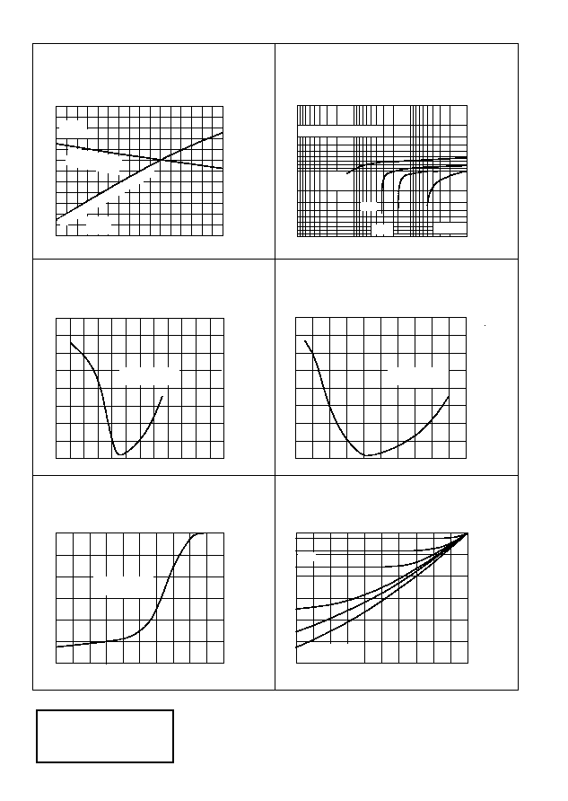
TYPICAL CHARACTERISTICS
0
-2
-4
-6
-8
-10
-1.2
Transfer Characteristics
V
DS
=-10V
300
µ
s Pulsed Test
I
D
-
Drain Cur
r
e
nt
(
Am
ps)
V
GS
- Gate Source
Voltage (Volts)
-0.8
-0.6
-0.4
0
-0.2
-1.0
0
-2
-4
-6
-8
-10
-1.2
Saturation Characteristics
I
D
- Drain Curre
n
t (Amps)
V
DS
- Drain Source
Voltage (Volts)
-0.8
-0.6
-0.4
0
-0.2
-1.0
300
µ
s Pulsed Test
V
GS
=-10V
-5V
-4V
-3V
-2.5V
-2V
Transconductance v drain current
I
D
- Drain Current (Amps
)
g
fs
-
T
r
a
n
s
c
o
n
d
ucta
nce (
m
S
)
300
0
-0.2
-0.4
-0.6
-0.8
-1.0
400
Transconductance v gate-source voltage
V
GS
-Gate Source Voltage (Volts)
g
fs
-
T
r
a
n
s
c
o
n
d
ucta
nce
(
m
S
)
0
-2
-4
-6
300
µ
s Pulsed Test
V
DS
=-10V
300
µ
s Pulsed Test
V
DS
=-10V
Normalised R
DS(on)
and V
GS(th)
vs Temperature
Junction Temperature (∞C)
Normali
s
ed R
D
S(o
n
)
a
nd
V
G
S(
t
h
)
-50
-25
0
25
50
75
125
100
150
2.4
2.2
2.0
1.8
1.6
1.4
1.2
1.0
0.6
0.8
Drai
n-
So
urce
R
esi
sta
nc
e R
DS(
on)
Gate Thres
hold
Voltage V
GS(TH)
On-resistance vs Drain Current
I
D-
Drain Current
(Amps)
R
D
S(on
)
-
D
r
a
i
n
So
u
rce
O
n
Re
s
istan
c
e
(
)
-2.5V
-3V
V
GS=
-10V
I
D=
-1mA
V
GS=
V
DS
-10V
10
1
100
-0.01
-0.1
-10
V
GS
=-2V
300
µ
s Pulsed Test
-1
I
D
=0.2A
0.2
0.4
0.0
200
100
0
300
400
200
100
0
C
rss
C
oss
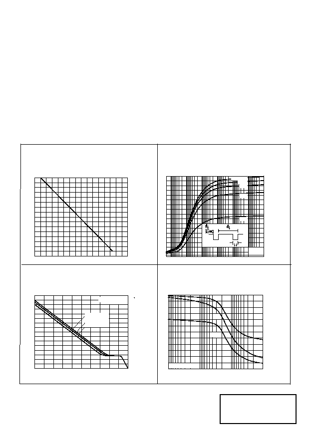
TYPICAL CHARACTERISTICS
0
1
4
5
-6
-8
-10
-14
-16
-12
-4
-2
0
Q-Gate Charge (nC)
200
150
100
0
50
250
300
-0.01
-1
-10
-100
V
DS
-Drain Source Voltage (Volts)
Capacitance v drain-source voltage
C-Capa
c
ita
n
ce (
p
F
)
Note:V
GS=
0V
C
iss
V
GS
-
G
a
te S
o
urc
e
V
oltage
(V
olts)
Gate charge v gate-source voltage
V
DS
= -20V
-50V
-100V
Note:I
D=-
0.25A
3
2
0.0001
50
150
100
Maximum transient thermal impedance
Pulse Width (seconds)
Thermal Resistance (∞C/W)
10
100
1
0.1
0.01
D=1 (D.C.)
D=0.5
D=0.2
D=0.1
Single Pulse
0.001
0
D=0.05
Derating Curve
T
amb
- Ambient Temperature (∞C)
P
to
t
-Power Dissipation (mW)
0.8
150
0.6
0.4
0.2
0
100
50
0
3-438
ZVP4424A
3-437
ZVP4424A
TYPICAL CHARACTERISTICS
0
-2
-4
-6
-8
-10
-1.2
Transfer Characteristics
V
DS
=-10V
300
µ
s Pulsed Test
I
D
-
Drain Cur
r
e
nt
(
Am
ps)
V
GS
- Gate Source
Voltage (Volts)
-0.8
-0.6
-0.4
0
-0.2
-1.0
0
-2
-4
-6
-8
-10
-1.2
Saturation Characteristics
I
D
- Drain Curre
n
t (Amps)
V
DS
- Drain Source
Voltage (Volts)
-0.8
-0.6
-0.4
0
-0.2
-1.0
300
µ
s Pulsed Test
V
GS
=-10V
-5V
-4V
-3V
-2.5V
-2V
Transconductance v drain current
I
D
- Drain Current (Amps
)
g
fs
-
T
r
a
n
s
c
o
n
d
ucta
nce (
m
S
)
300
0
-0.2
-0.4
-0.6
-0.8
-1.0
400
Transconductance v gate-source voltage
V
GS
-Gate Source Voltage (Volts)
g
fs
-
T
r
a
n
s
c
o
n
d
ucta
nce
(
m
S
)
0
-2
-4
-6
300
µ
s Pulsed Test
V
DS
=-10V
300
µ
s Pulsed Test
V
DS
=-10V
Normalised R
DS(on)
and V
GS(th)
vs Temperature
Junction Temperature (∞C)
Normali
s
ed R
D
S(o
n
)
a
nd
V
G
S(
t
h
)
-50
-25
0
25
50
75
125
100
150
2.4
2.2
2.0
1.8
1.6
1.4
1.2
1.0
0.6
0.8
Drai
n-
So
urce
R
esi
sta
nc
e R
DS(
on)
Gate Thres
hold
Voltage V
GS(TH)
On-resistance vs Drain Current
I
D-
Drain Current
(Amps)
R
D
S(on
)
-
D
r
a
i
n
So
u
rce
O
n
Re
s
istan
c
e
(
)
-2.5V
-3V
V
GS=
-10V
I
D=
-1mA
V
GS=
V
DS
-10V
10
1
100
-0.01
-0.1
-10
V
GS
=-2V
300
µ
s Pulsed Test
-1
I
D
=0.2A
0.2
0.4
0.0
200
100
0
300
400
200
100
0
C
rss
C
oss
TYPICAL CHARACTERISTICS
0
1
4
5
-6
-8
-10
-14
-16
-12
-4
-2
0
Q-Gate Charge (nC)
200
150
100
0
50
250
300
-0.01
-1
-10
-100
V
DS
-Drain Source Voltage (Volts)
Capacitance v drain-source voltage
C-Capa
c
ita
n
ce (
p
F
)
Note:V
GS=
0V
C
iss
V
GS
-
G
a
te S
o
urc
e
V
oltage
(V
olts)
Gate charge v gate-source voltage
V
DS
= -20V
-50V
-100V
Note:I
D=-
0.25A
3
2
0.0001
50
150
100
Maximum transient thermal impedance
Pulse Width (seconds)
Thermal Resistance (∞C/W)
10
100
1
0.1
0.01
D=1 (D.C.)
D=0.5
D=0.2
D=0.1
Single Pulse
0.001
0
D=0.05
Derating Curve
T
amb
- Ambient Temperature (∞C)
P
to
t
-Power Dissipation (mW)
0.8
150
0.6
0.4
0.2
0
100
50
0
3-438
ZVP4424A
3-437
ZVP4424A