1
ISSUE 1 - MARCH 2001
ZVP4525G
SUMMARY
(
DESCRIPTION
This 250V enhancement mode N-channel MOSFET provides users with a
competitive specification offering efficient power handling capability, high
impedance and is free from thermal runaway and thermally induced
secondary breakdown. Applications benefiting from this device include a
variety of Telecom and general high voltage circuits.
SOT89 and SOT23-6 versions are also available.
FEATURES
∑
High voltage
∑
Low on-resistance
∑
Fast switching speed
∑
Low gate drive
∑
Low threshold
∑
Complementary P-channel Type ZVN4525G
∑
SOT223 package
APPLICATIONS
∑
Earth Recall and dialling switches
∑
Electronic hook switches
∑
High Voltage Power MOSFET Drivers
∑
Telecom call routers
∑
Solid state relays
ORDERING INFORMATION
DEVICE
REEL SIZE
(inches)
TAPE WIDTH (mm)
QUANTITY
PER REEL
ZVP4525GTA
7
8mm embossed
1000 units
ZVP4525GTC
13
8mm embossed
4000 units
DEVICE MARKING
∑
ZVP4525G
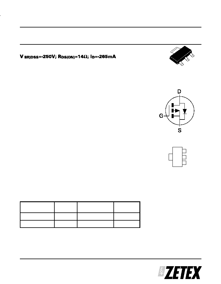
250V P-CHANNEL ENHANCEMENT MODE MOSFET
D
D
S
G
Top View
SOT223

ISSUE 1 - MARCH 2001
ZVP4525G
2
THERMAL RESISTANCE
PARAMETER
SYMBOL
VALUE
UNIT
Junction to Ambient (a)
R
JA
63
∞C/W
Junction to Ambient (b)
R
JA
26
∞C/W
NOTES
(a) For a device surface mounted on 25mm x 25mm FR4 PCB with high coverage of single sided 1oz copper,
in still air conditions
(b) For a device surface mounted on FR4 PCB measured at t 5 secs.
(c) Repetitive rating - pulse width limited by maximum junction temperature. Refer to Transient Thermal
Impedance graph.
ABSOLUTE MAXIMUM RATINGS.
PARAMETER
SYMBOL
LIMIT
UNIT
Drain-Source Voltage
V
DSS
250
V
Gate Source Voltage
V
GS
±
40
V
Continuous Drain Current (V
GS
=10V; TA=25∞C)(a)
(V
GS
=10V; TA=70∞C)(a)
I
D
I
D
-265
-212
mA
mA
Pulsed Drain Current (c)
I
DM
-1
A
Continuous Source Current (Body Diode)
I
S
-0.75
A
Pulsed Source Current (Body Diode)
I
SM
-1
A
Power Dissipation at T
A
=25∞C (a)
Linear Derating Factor
P
D
2
16
W
mW/∞C
Operating and Storage Temperature Range
T
j
:
T
stg
-55 to +150
∞C
NB High Voltage Applications
For high voltage applications, the appropriate industry sector guidelines should be considered with regard to
voltage spacing between conductors.

ISSUE 1 - MARCH 2001
ZVP4525G
3
CHARACTERISTICS

ISSUE 1 - MARCH 2001
ZVP4525G
4
ELECTRICAL CHARACTERISTICS (at T
amb
= 25∞C unless otherwise stated).
PARAMETER
SYMBOL MIN.
TYP.
MAX.
UNIT CONDITIONS.
STATIC
Drain-Source Breakdown Voltage
V
(BR)DSS
-250
-285
V
I
D
=-1mA, V
GS
=0V
Zero Gate Voltage Drain Current
I
DSS
-30
-500
nA
V
DS
=-250V, V
GS
=0V
Gate-Body Leakage
I
GSS
±1
±100
nA
V
GS
=
±
40V, V
DS
=0V
Gate-Source Threshold Voltage
V
GS(th)
-0.8
-1.5
-2.0
V
I
D
=-1mA, V
DS
= V
GS
Static Drain-Source On-State Resistance (1)
R
DS(on)
10
13
14
18
V
GS
=-10V, I
D
=-200mA
V
GS
=-3.5V, I
D
=-100mA
Forward Transconductance (3)
g
fs
80
200
mS
V
DS
=-10V,I
D
=-0.15A
DYNAMIC (3)
Input Capacitance
C
iss
73
pF
V
DS
=-25 V, V
GS
=0V,
f=1MHz
Output Capacitance
C
oss
12.8
pF
Reverse Transfer Capacitance
C
rss
3.91
pF
SWITCHING(2) (3)
Turn-On Delay Time
t
d(on)
1.53
ns
V
DD
=-30V, I
D
=-200mA
R
G
=50
, V
GS
=-10V
(refer to test circuit)
Rise Time
t
r
3.78
ns
Turn-Off Delay Time
t
d(off)
17.5
ns
Fall Time
t
f
7.85
ns
Total Gate Charge
Q
g
2.45
3.45
nC
V
DS
=-25V,V
GS
=-10V,
I
D
=-200mA(refer to
test circuit)
Gate-Source Charge
Q
gs
0.22
0.31
nC
Gate Drain Charge
Q
gd
0.45
0.63
nC
SOURCE-DRAIN DIODE
Diode Forward Voltage (1)
V
SD
0.97
V
T
j
=25∞C, I
S
=-200mA,
V
GS
=0V
Reverse Recovery Time (3)
t
rr
205
290
ns
T
j
=25∞C, I
F
=-200mA,
di/dt= 100A/
µ
s
Reverse Recovery Charge (3)
Q
rr
21
29
nC
(1) Measured under pulsed conditions. Width=300
µ
s. Duty cycle
2% .
(2) Switching characteristics are independent of operating junction temperature.
(3) For design aid only, not subject to production testing.

ISSUE 1 - MARCH 2001
ZVP4525G
5
TYPICAL CHARACTERISTICS