 | –≠–ª–µ–∫—Ç—Ä–æ–Ω–Ω—ã–π –∫–æ–º–ø–æ–Ω–µ–Ω—Ç: ZVP4525TC | –°–∫–∞—á–∞—Ç—å:  PDF PDF  ZIP ZIP |
1
ISSUE 1 - MARCH 2001
ZVP4525E6
SUMMARY
(
DESCRIPTION
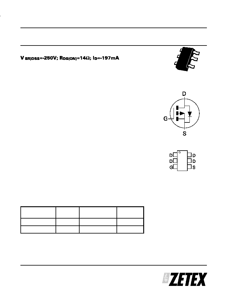
This 250V enhancement mode P-channel MOSFET provides users with a
competitive specification offering efficient power handling capability, high
impedance and is free from thermal runaway and thermally induced
secondary breakdown. Applications benefiting from this device include a
variety of Telecom and general high voltage circuits.
SOT89 and SOT223 versions are also available.
FEATURES
∑
High voltage
∑
Low on-resistance
∑
Fast switching speed
∑
Low gate drive
∑
Low threshold
∑
Complementary N-channel Type ZVN4525E6
∑
SOT23-6 package
APPLICATIONS
∑
Earth Recall and dialling switches
∑
Electronic hook switches
∑
High Voltage Power MOSFET Drivers
∑
Telecom call routers
∑
Solid state relays
ORDERING INFORMATION
DEVICE
REEL SIZE
(inches)
TAPE WIDTH (mm)
QUANTITY
PER REEL
ZVP4525TA
7
8mm embossed
3000 units
ZVP4525TC
13
8mm embossed
10000 units
DEVICE MARKING
∑
P52
250V P-CHANNEL ENHANCEMENT MODE MOSFET
Top View
SOT23-6
ISSUE 1 - MARCH 2001
ZVP4525E6
2
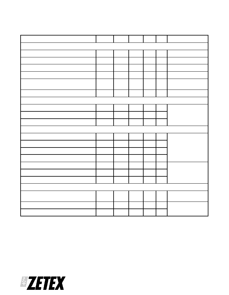
ABSOLUTE MAXIMUM RATINGS.
PARAMETER
SYMBOL
LIMIT
UNIT
Drain-Source Voltage
V
DSS
-250
V
Gate Source Voltage
V
GS
±
40
V
Continuous Drain Current (V
GS
=10V; TA=25∞C)(a)
(V
GS
=10V; TA=70∞C)(a)
I
D
I
D
-197
-157
mA
mA
Pulsed Drain Current (c)
I
DM
-1
A
Continuous Source Current (Body Diode)
I
S
-0.75
A
Pulsed Source Current (Body Diode)
I
SM
-1
A
Power Dissipation at T
A
=25∞C (a)
Linear Derating Factor
P
D
1.1
8.8
W
mW/∞C
Operating and Storage Temperature Range
T
j
:
T
stg
-55 to +150
∞C
THERMAL RESISTANCE
PARAMETER
SYMBOL
VALUE
UNIT
Junction to Ambient (a)
R
JA
113
∞C/W
Junction to Ambient (b)
R
JA
68
∞C/W
NOTES
(a) For a device surface mounted on 25mm x 25mm FR4 PCB with high coverage of single sided 1oz copper,
in still air conditions
(b) For a device surface mounted on FR4 PCB measured at t 5 secs.
(c) Repetitive rating - pulse width limited by maximum junction temperature. Refer to Transient Thermal
Impedance graph.
NB High Voltage Applications
For high voltage applications, the appropriate industry sector guidelines should be considered with regard to
voltage spacing between conductors.
ISSUE 1 - MARCH 2001
ZVP4525E6
3
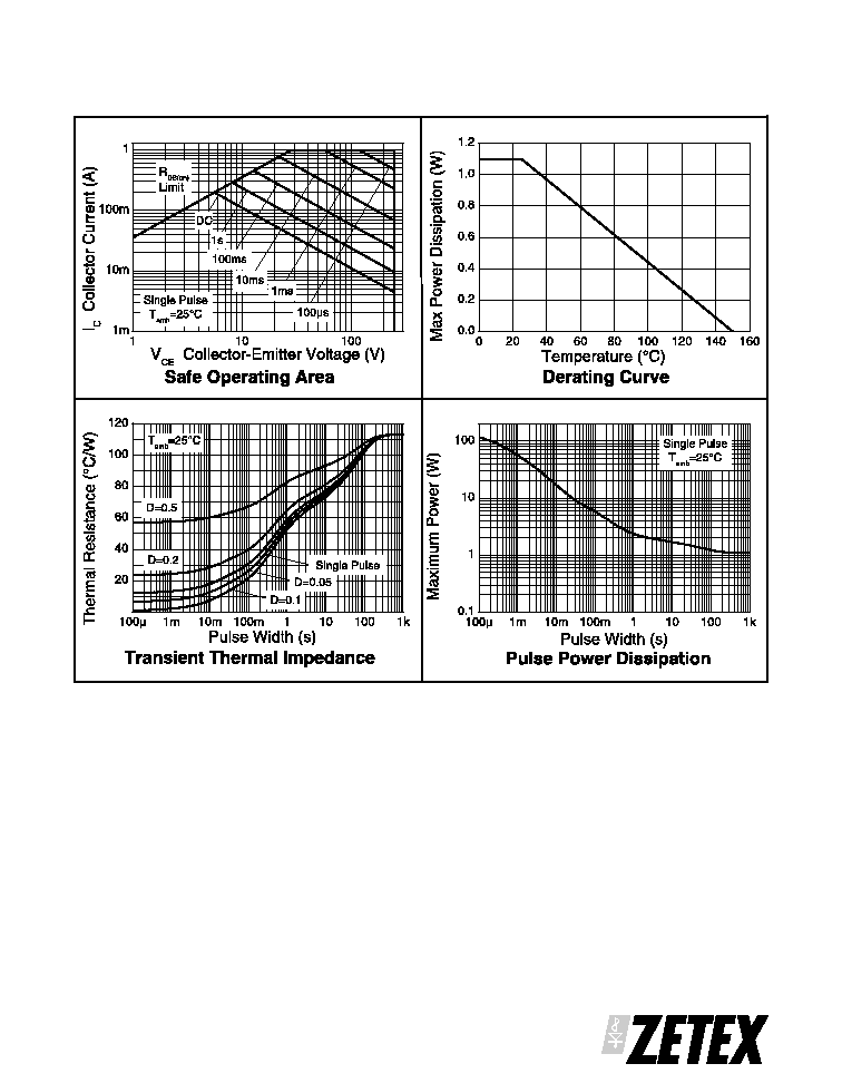
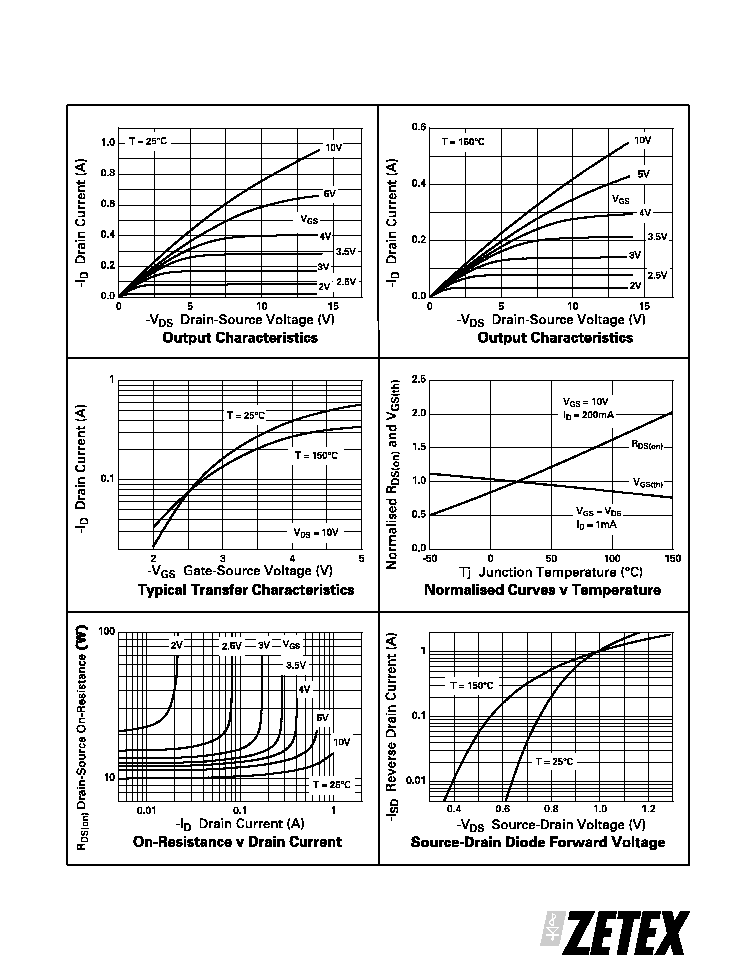
CHARACTERISTICS
ISSUE 1 - MARCH 2001
ZVP4525E6
4
ELECTRICAL CHARACTERISTICS (at T
amb
= 25∞C unless otherwise stated).
PARAMETER
SYMBOL MIN.
TYP.
MAX.
UNIT CONDITIONS.
STATIC
Drain-Source Breakdown Voltage
V
(BR)DSS
-250
-285
V
I
D
=-1mA, V
GS
=0V
Zero Gate Voltage Drain Current
I
DSS
-30
-500
nA
V
DS
=-250V, V
GS
=0V
Gate-Body Leakage
I
GSS
±1
±100
nA
V
GS
=
±
40V, V
DS
=0V
Gate-Source Threshold Voltage
V
GS(th)
-0.8
-1.5
-2.0
V
I
D
=-1mA, V
DS
= V
GS
Static Drain-Source On-State Resistance (1)
R
DS(on)
10
13
14
18
V
GS
=-10V, I
D
=-200mA
V
GS
=-3.5V, I
D
=-100mA
Forward Transconductance (3)
g
fs
80
200
mS
V
DS
=-10V,I
D
=-0.15A
DYNAMIC (3)
Input Capacitance
C
iss
73
pF
V
DS
=-25 V, V
GS
=0V,
f=1MHz
Output Capacitance
C
oss
12.8
pF
Reverse Transfer Capacitance
C
rss
3.91
pF
SWITCHING(2) (3)
Turn-On Delay Time
t
d(on)
1.53
ns
V
DD
=-30V, I
D
=-200mA
R
G
=50
, V
GS
=-10V
(refer to test circuit)
Rise Time
t
r
3.78
ns
Turn-Off Delay Time
t
d(off)
17.5
ns
Fall Time
t
f
7.85
ns
Total Gate Charge
Q
g
2.45
3.45
nC
V
DS
=-25V,V
GS
=-10V,
I
D
=-200mA(refer to
test circuit)
Gate-Source Charge
Q
gs
.22
.31
nC
Gate Drain Charge
Q
gd
.45
.63
nC
SOURCE-DRAIN DIODE
Diode Forward Voltage (1)
V
SD
0.97
V
T
j
=25∞C, I
S
=-200mA,
V
GS
=0V
Reverse Recovery Time (3)
t
rr
205
290
ns
T
j
=25∞C, I
F
=-200mA,
di/dt= 100A/
µ
s
Reverse Recovery Charge (3)
Q
rr
21
29
nC
(1) Measured under pulsed conditions. Width=300
µ
s. Duty cycle
2% .
(2) Switching characteristics are independent of operating junction temperature.
(3) For design aid only, not subject to production testing.
ISSUE 1 - MARCH 2001
ZVP4525E6
5
TYPICAL CHARACTERISTICS