 | –≠–ª–µ–∫—Ç—Ä–æ–Ω–Ω—ã–π –∫–æ–º–ø–æ–Ω–µ–Ω—Ç: ZXBM2002 | –°–∫–∞—á–∞—Ç—å:  PDF PDF  ZIP ZIP |
DESCRIPTION
The ZXBM200x is a series of 2-phase, DC brushless motor pre-drivers with PWM
variable speed control suitable for fan and blower motors.
FEATURES
∑
Built in lock detect protection, rotational speed sensing and automatic recovery
∑
Built in Hall amplifier allows direct connection to Hall element
∑
PWM Speed control can be implemented via external voltage or resistance (thermistor) input
∑
Speed (FG) pulse output ≠ ZXBM2003
∑
Rotor lock output ≠ ZXBM2002
∑
Combined Rotor Lock (RD) and Speed (FG) signal ≠ ZXBM2001
∑
Up to 18V input voltage (60V with external regulator)
∑
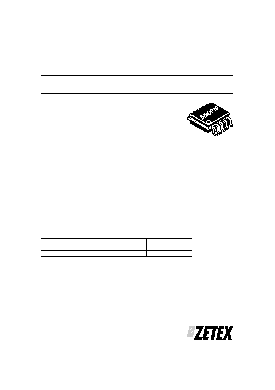
MSOP10 package
APPLICATIONS
∑
Mainframe and Personal Computer Fans and Blowers
∑
Instrumentation Fans
∑
Central Heating Blowers
∑
Automotive climate control
DEVICE MARKING
ZXBM2001 - BM21
ZXBM2002 - BM22
ZXBM2003 - BM23
ZXBM2001
ZXBM2002 ZXBM2003
ISSUE 1 - APRIL 2002
1
VARIABLE SPEED 2-PHASE FAN MOTOR CONTROLLER
DEVICE
REEL SIZE
TAPE WIDTH
QUANTITY PER REEL
ZXBM200xX10TA
7" (180mm)
12mm
1,000
ZXBM200xX10TC
13" (330mm)
12mm
4,000
ORDERING INFORMATION
Example: ZXBM2001X10TA
ZXBM2001
ZXBM2002 ZXBM2003
ISSUE 1 - APRIL 2002
2
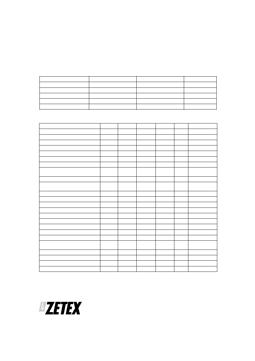
Parameter
Symbol
Limits
Unit
Supply Voltage
V
CCmax
-0.6 to 20
V
Input Current
I
CC
200
mA
Power Dissipation
P
D
500
mW
Operating Temp.
T
OPR
-40 to 85
C
Storage Temp.
T
STG
-55 to 125
C
Absolute maximum ratings
Parameter
Symbol
Min
Typ
Max
Unit
Conditions
Supply Voltage
V
CC
4.5
18
V
Supply Current
I
CC
2.2
3.25
mA
No Load
1
Hall Amp Input Voltage
40
mV
diff p-p
Hall Amp Common Mode Voltage
V
CM
0.5
0.5V
CC
V
CC
-1.5
V
Hall Amp Input Offset
V
OFS
±7
mV
Hall Amp Bias Current
V
BS
-350
nA
PH1, PH2 Output High
V
OH
V
CC
-2.2
V
CC
-1.8
V
I
OH
= 80mA
PH1, PH2 Output Off Leakage
Current
I
OFF
10
A
PH1, PH2 Output Current
I
OL
80
mA
Lock/FG Maximum Collector
Voltage
V
OH
V
CC
V
Lock/FG Sink Current
I
OL
5
mA
Lock/FG Low Level O/P Voltage
V
OL
0.3
0.5
V
I
OL
= 5mA
C
LCK
Charge Current
I
LCKC
-1.8
-2.8
A
V
in
= 1.5V
C
LCK
Discharge Current
I
LCKD
0.28
0.35
A
V
in
= 1.5V
Lock condition On:Off ratio
1:7
1:10
C
LCK
High Threshold Voltage
V
THH
2.0
V
C
LCK
Low Threshold Voltage
V
THL
1.0
V
C
PWM
Charge Current
I
PWMC
3.6
4.3
5.0
A
V
in
= 1.5V
C
PWM
Discharge Current
I
PWMD
50
62
75
A
V
in
= 1.5V
PWM Frequency
F
PWM
24
kHz
C
PWM
=
0.15nF
C
PWM
High Threshold Voltage
V
THH
2.0
V
C
PWM
Low Threshold Voltage
V
THL
1.0
V
SPD Voltage Control Range
V
SPD
1
2
V
2
SPD Open Circuit Voltage
1.5
V
3
Electrical Characteristics (at Tamb = 25∞C & Vcc = 12V)
Notes:
1
Measured with pins H+, H-, CLCK and CPWM = 0V and all other signal pins open circuit.
2
The 1V minimum represents 100% PWM drive and 2V represents 0% PWM drive.
3
This voltage is determined by an internal resistor network of 52.5k
from the pin to Gnd and 19.5k
from the pin to a 2V reference. Whilst both
resistors track each other the absolute values are subject to a
20% manufacturing tolerance.
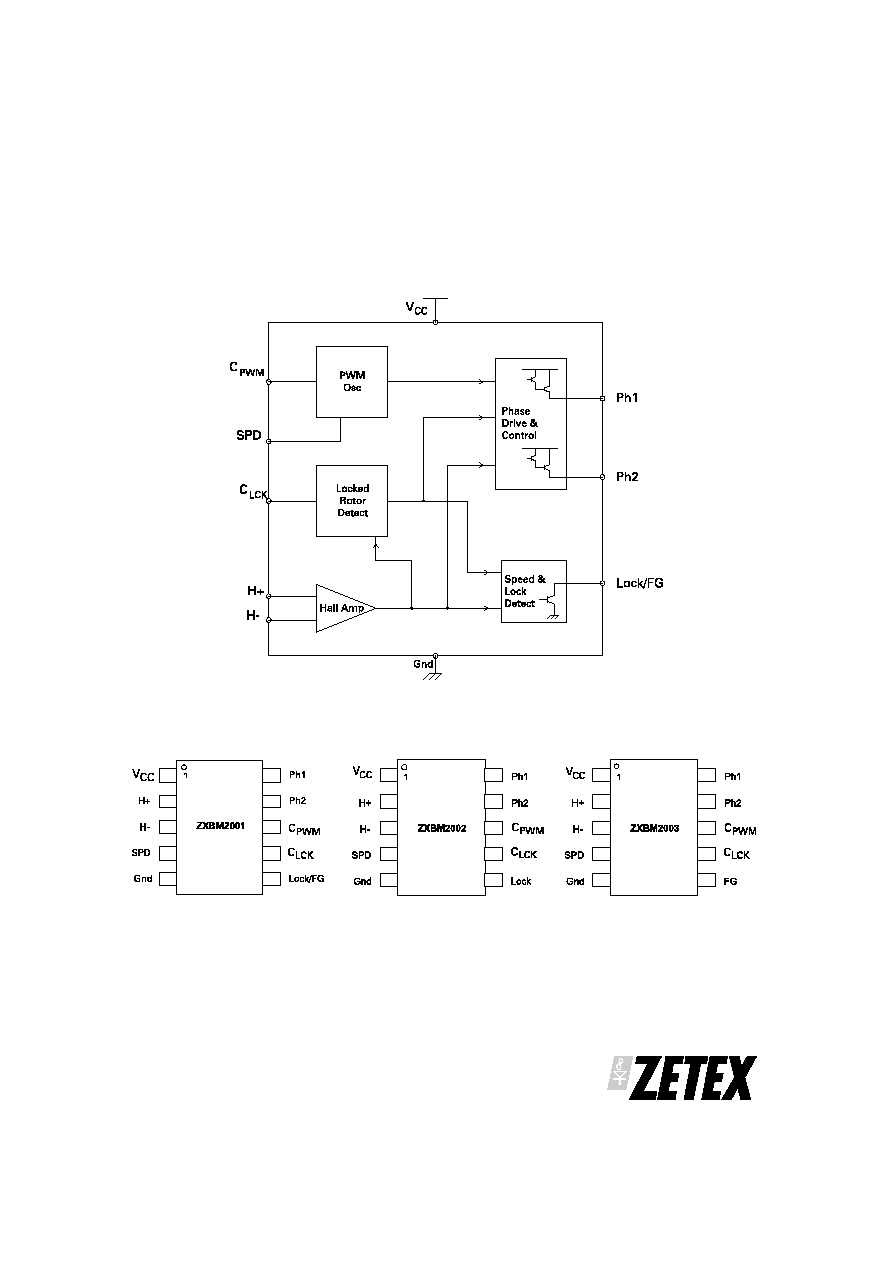
Block Diagram (ZXBM2001):
Pin Assignments
ZXBM2001
ZXBM2002 ZXBM2003
ISSUE 1 - APRIL 2002
3

Pin Functional Descriptions
1. VCC
- Applied voltage
This is the device supply voltage. For 5V to 12V fans this
can be supplied directly from the Fan Motor supply. For
fans likely to run in excess of the 18V maximum rating
for the device this will be supplied from an external
regulator such as a zener diode.
2. H+
- Hall input
3. H-
- Hall input
The rotor position of the Fan Motor is detected by a Hall
sensor whose output is applied to these pins. This
sensor can be either a 4 pin `naked' Hall device or a 3
pin buffered switching type. For a 4 pin device the
differential Hall output signal is connected to the H+
and H- pins. For a 3 pin buffered Hall sensor the Hall
device output is attached to the H+ pin whilst the H- pin
has an external potential divider attached to hold the
pin at half V
CC
. When H+ is high in relation to H- Ph2 is
the active drive.
4. SPD
- Speed control voltage input
This pin provides control over the Fan Motor speed by
varying the Pulse Width Modulated (PWM) drive ratio
at the Ph1 and Ph2 outputs. This control signal can take
the form of either a voltage input of nominal range 2V
to 1V, representing 0% to 100% drive respectively, or
alternatively a thermistor can be attached to this pin to
control the voltage. The pin has an internal potential
divider between Gnd and an internal 2.0V reference
designed to hold the pin at approximately 1.5V. This
will represent a drive of nominally 50%. The addition of
a 100k NTC thermistor to ground, for example, will
provide a drive nominally 70% at 25∞C and 100% at
50∞C.
If speed control is not required this pin is can be left
open circuit for 50% drive or tied to ground by a 10k
resistor to provide 100% drive.
If required this pin can also be used as an enable pin.
The application of a voltage of 2.0V to V
CC
will to force
the PWM drive fully off, in effect disabling the drive.
5. GND
- Ground
This is the device supply ground return pin and will
generally be the most negative supply pin to the fan.
6. LOCK/FG
- Locked Rotor error output /
Frequency Generator (speed) output
On the ZXBM2001 the Lock/FG pin is designed to be a
dual function pin to provide an indication of the Fans
rotational speed together with an indication of when
the Fan has failed rotating for whatever reason (Rotor
Locked condition). The pin is an open collector drive,
that is there is an active pull down with the high level
being provided by an external pull up resistor. Under
correct operating conditions, and with this external
pull-up in place, this pin will provide an output signal
whose frequency will be twice that of the rotational
frequency of the fan. Should the fan itself stop rotating
for any reason, i.e. an obstruction in the fan blade or a
seized bearing, then the device will enter a Rotor
Locked condition. In this condition the Lock/FG pin will
go high (regardless of the state of the Hall sensor)
when the C
LCK
pin reaches the V
THH
threshold and will
remain high until the fan blades start rotating again.
On the ZXBM2002 variant this pin is Lock. During
normal operation the signal will be low and during a
Locked Rotor condition the pin will go high when the
C
LCK
pin reaches the V
THH
threshold.
For the ZXBM2003 variant this pin is FG. This signal is a
buffered and inverted output of the Hall signal and
therefore provides an output signal whose frequency
will be twice that of the rotational frequency of the fan.
7. C
LCK
- Locked Rotor timing capacitor
When in a Locked Rotor condition as described above
the Ph1 and Ph2 drive outputs go into a safe drive mode
to protect the external drive devices and the motor
windings. This condition consists of driving the motor
for a short period then waiting for a longer period
before trying again. The frequency at which this takes
place is determined by the size of the capacitor applied
to this CLCK pin. For a 12V supply a value of 1.0uF will
typically provide an `On' (drive) period of 0.33s and an
`Off' (wait) period of 4.0s, giving an On:Off ratio of 1:12.
ZXBM2001
ZXBM2002 ZXBM2003
ISSUE 1 - APRIL 2002
4
Locked Rotor timing capacitor (CONT).
The C
LCK
timing periods are determined by the
following equations:
T
V
C
I
THH
LCK
LCKC
lock
=
◊
T
V
V
C
I
THH
THL
LCK
LCKD
off
=
-
◊
(
)
T
V
V
C
I
THH
THL
LCK
LCKC
on
=
-
◊
(
)
Where V
THH
and V
THL
are the C
LCK
pin threshold
voltages and I
LCKC
and I
LCKD
are the charge and
discharge currents.
As these threshold voltages are nominally set to
V
THH
=2V and V
THL
=1V the equations can be simplified
as follows:
T
C
I
LCK
LCKC
lock
=
◊
2
T =
C
I
on
LCK
LCKC
T
C
I
LCK
LCKD
off
=
8. C
PWM
- Sets PWM frequency
This pin has an external capacitor attached to set the
PWM frequency for the Phase drive outputs. A
capacitor value of 0.15nF will provide a PWM
frequency of typically 24kHz.
The C
LCK
timing period (T
pwm
) is determined by the
following equation:
T
V
V
C
I
V
V
C
I
THH
THL
PWM
PWMC
THH
THL
PWM
PWMD
pwm
=
-
◊
+
-
◊
(
)
(
)
Where V
THH
and V
THL
are the C
PWM
pin threshold
voltages and I
PWMC
and I
PWMD
are the charge and
discharge currents.
As these threshold voltages are nominally set to
V
THH
=2V and V
THL
=1V the equations can be simplified
as follows:
T
C
I
C
I
PWM
PWMC
PWM
PWMD
pwm
=
+
9. PH2
- External transistor driver
10. PH1
- External transistor driver
These are the Phase drive outputs and are open
darlington emitter followers designed to provide up to
80mA of drive to external transistors as shown in the
Application circuits following. The external transistors
in turn drive the fan motor windings.
Lock Timing Example:
Using the equation previously described and to be
found under the C
LCK
pin description:
T
C
I
LCK
LCKC
lock
=
◊
2
T
C
I
LCK
LCKC
on
=
T
C
I
LCK
LCKD
off
=
Using a value of C
LCK
= 1.0uF together with the values
of I
LCKC
and I
LCKD
to be found in the Electrical
Characteristics we can derive the following timings for
operation at 12V and 25∞C.
T
=
2 1.0 F
2.8 A
lock
◊
=
0 714
.
s
T
=
1.0 F
0.28 A
off
=
3 6
.
s
T =
2 1.0 F
2.8 A
on
◊
=
0 36
.
s
ZXBM2001
ZXBM2002 ZXBM2003
ISSUE 1 - APRIL 2002
5
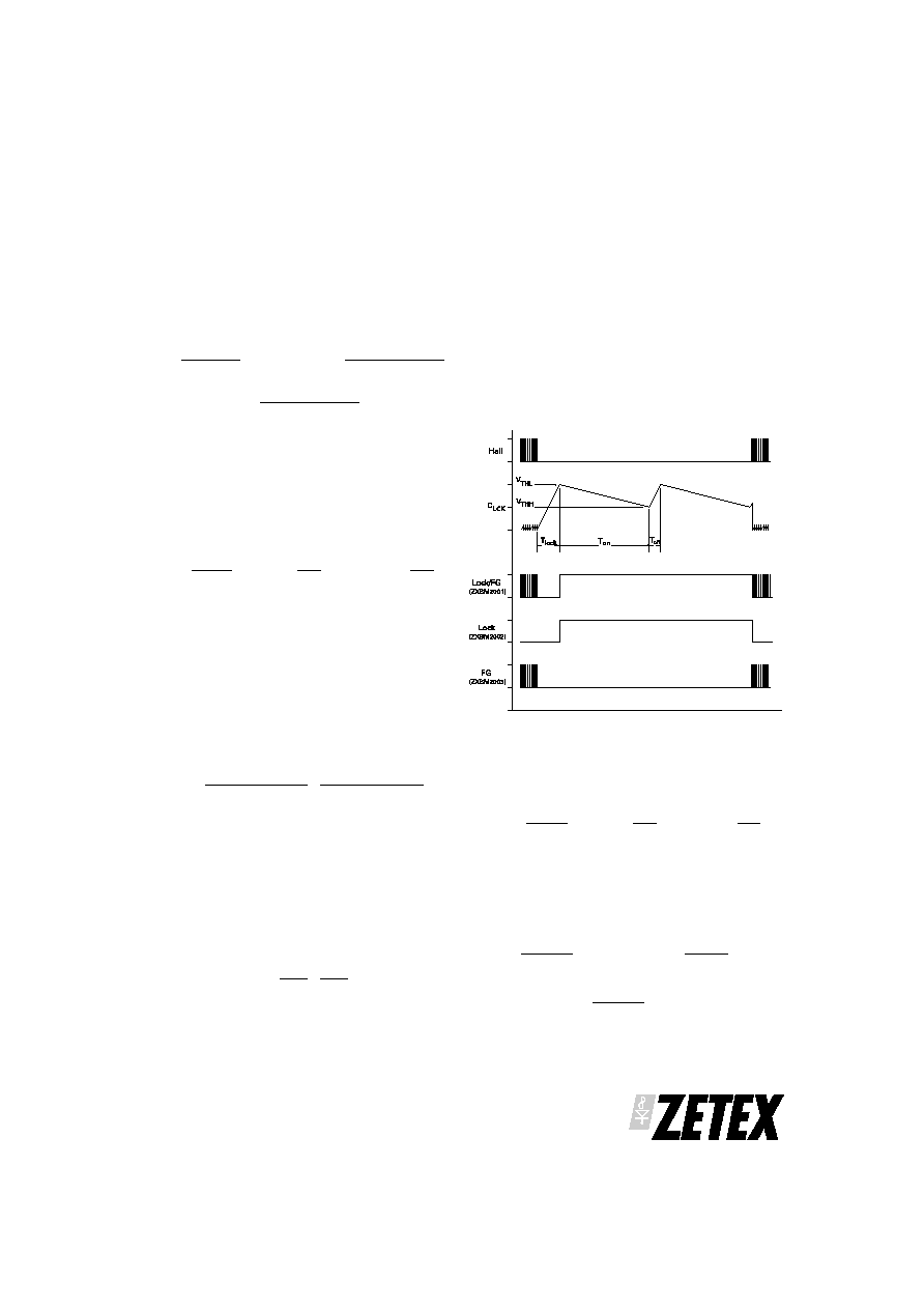
Lock and FG Timing Waveform: