S E M I C O N D U C T O R S
DESCRIPTION
The ZXCD1010 provides complete control and
modulation functions at the heart of a high efficiency
high performance Class D switching audio amplifier
solution.
In combination with matched output
magnetics and Zetex HDMOS MOSFET devices, the
ZXCD1010 provides a high performance Class D audio
amplifier with all the inherent benefits of Class D.
The ZXCD1010 is an enhanced version of the
ZXCD1000. The timing resistor for the oscillator is
taken off the chip enabling improved oscillator
frequency matching device to device.
The ZXCD1010 solution uses proprietary circuitry and
magnetic technology to realise the true benefits of
Class D without the traditional drawback of poor
distortion performance.
The combination of circuit
design, magnetic component choice and layout are
essential to realising these benefits.
FEATURES
∑
90% efficiency
∑
External R
OSC
C
OSC
for improved accuracy
∑
4 / 8
drive capability
∑
Noise Floor -115dB for solution
∑
Flat response 20Hz - 20kHz
∑
High gate drive capability ( 2200pF)
∑
Very low THD + N 0.2% typical of full power up to
90% ( for the solution)
∑
Complete absence of crossover artifacts
∑
OSC output available for sync in multi-channel
applications
∑
Available in a 16 pin exposed pad QSOP package
∑
Refer to ZXCD1000 data sheet for typical
characteristics and applications indormation
The ZXCD1010 reference designs give output powers
up to 100W rms with typical open loop (no feedback)
distortions of less than 0.2% THD + N over the entire
audio frequency range at 90% full output power. This
gives an extremely linear system. The addition of a
minimum amount of feedback (10dB) further reduces
distortion figures to give < 0.1 % THD + N typical at
1kHz.
From an acoustic point of view, even more important
than the figures above, the residual distortion is almost
totally free of any crossover artifacts. This allows the
ZXCD1010 to be used in true hi-fi applications. This lack
of crossover distortion, sets the ZXCD1010 solutions
quite apart from most other presently available
solutions.
APPLICATIONS
∑
DVD receivers
∑
Automotive audio systems
∑
Home Theatre
∑
Multimedia
∑
Wireless speakers
∑
Portable audio
∑
Sub woofer systems
∑
Public Address systems
ZXCD1010
ISSUE 3 - NOVEMBER 2003
1
HIGH FIDELITY CLASS D AUDIO AMPLIFIER SOLUTION
Distortion v Power
(8
open loop at 1kHz.)
ABSOLUTE MAXIMUM RATINGS
Terminal Voltage with respect to G
ND
V
CC
20V
Power Dissipation
1W
Package Thermal Resistance (
ja
)
54 C/W
Operating Temperature Range
-40 C to 70 C
Maximum Junction Temperature
125 C
Storage Temperature Range
-50∞C to 85 C
Stresses beyond those listed under "Absolute Maximum Ratings" may cause permanent damage to the device.
These are stress ratings only, and functional operation of the device at these or any other conditions beyond
those indicated in the operational sections of the specifications is not implied. Exposure to absolute maximum
conditions for extended periods may affect device reliability.
ZXCD1010
S E M I C O N D U C T O R S
ISSUE 3 - NOVEMBER 2003
2
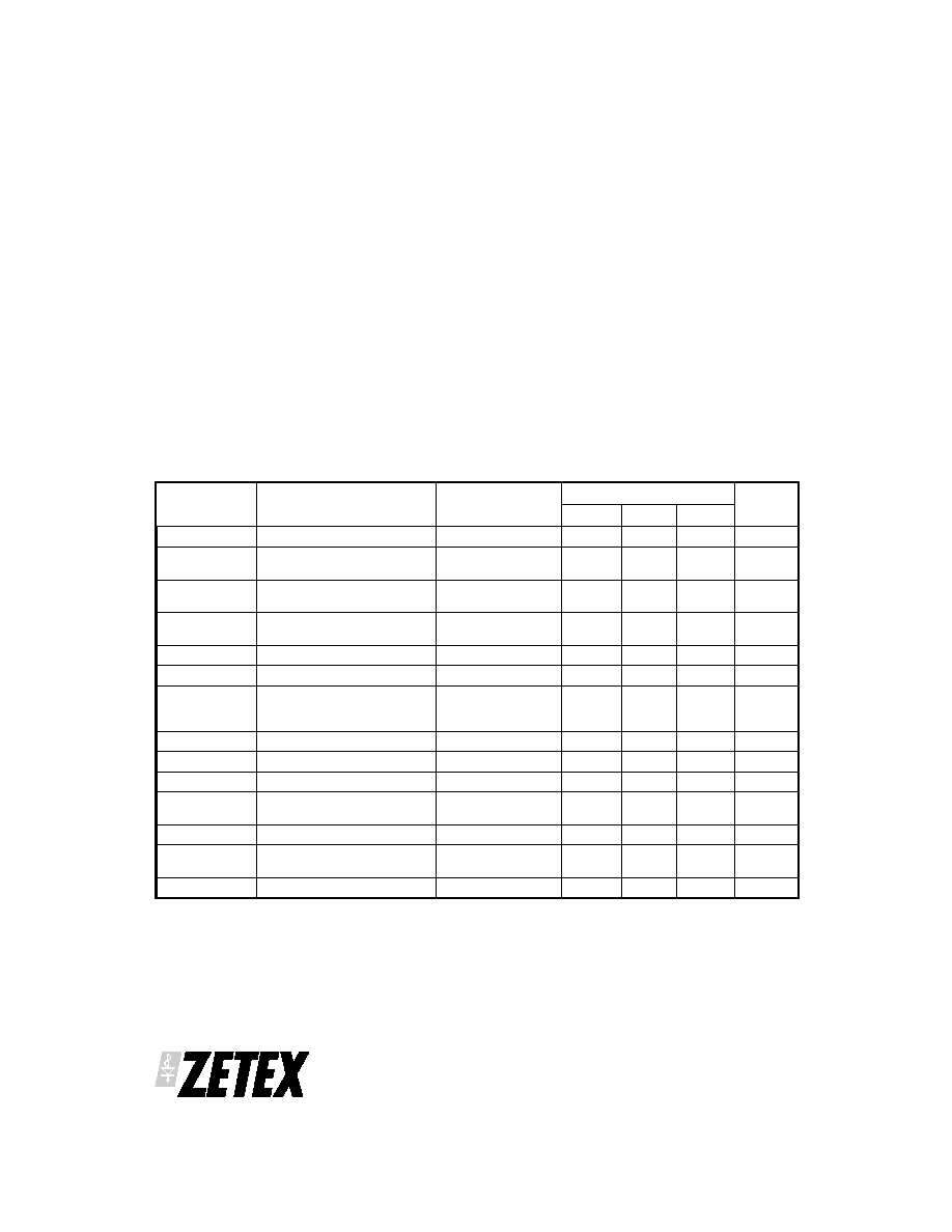
SYMBOL
PARAMETER
CONDITIONS
LIMITS
UNITS
MIN
TYP
MAX
V
CC
Operating Voltage Range
12
16
18
V
I
ss
Operating Quiescent
Current
V
CC
= 12V
V
CC
= 18V, 16V
45
50
mA
mA
F
osc
Switching Frequency
C
OSC
= 330pF,
R
OSC
= 31k5
173
192
211
kHz
F
osc(tol)
Frequency Tolerance
C
OSC
= 330pF,
R
OSC
= 31k5
+/-10
%
Vol OutA/B
Low level output voltage
No load
100
mV
Voh OutA/B
High level output voltage
No load
7.5
V
T
Drive
Output Drive Capability
(OUT A / B Rise/Fall)
Load
Capacitance
= 2200pF
50
ns
5V5tol
Internal Rail Tolerance
1µF Decoupling
5.16
5.5
5.77
V
9VA/Btol
Internal Rail Tolerance
1µF Decoupling
8.32
8.75
9.18
V
Audio A / B
Input Impedence
1.35k
1.8k
2.3k
Triangle
A / B
Input Impedence
1.35k
1.8k
2.3k
Audio A / B
Bias Level
2.95
3.1
3.25
V
Triangle
A / B
Bias Level
2.95
3.1
3.25
V
Osc A / B
Amplitude
0.89
1.05
1.2
V
ELECTRICAL CHARACTERISTICS
TEST CONDITIONS (unless otherwise stated) VCC = 16V, TA = 25∞C
ZXCD1010
S E M I C O N D U C T O R S
ISSUE 3 - NOVEMBER 2003
3
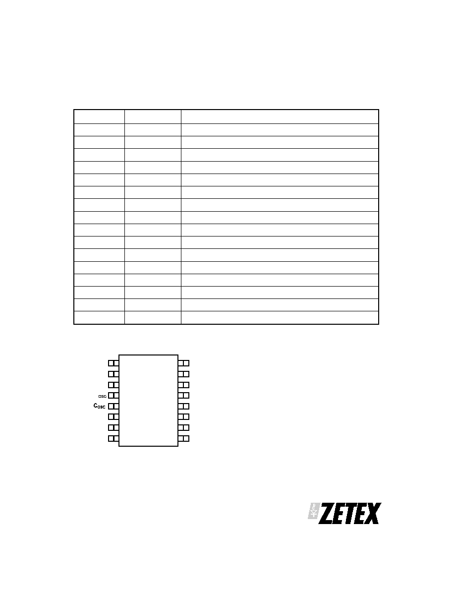
Pin number
Pin Name
Pin Description
1
Audio A
Audio Input for Channel A
2
Triangle A
Triangle Input for Channel A
3
Osc A
Triangle Output
4
R
OSC
External timing resistor node (to set the switching frequency)
5
C
osc
External timing capacitor node (to set the switching frequency)
6
Osc B
Triangle Output (for slave ZXCD1010 in stereo application)
7
Triangle B
Triangle Input for Channel B
8
Audio B
Audio Input for Channel B
9
Gnd
Small Signal GND
10
OUT B
Channel B PWM Output to drive external Bridge MOSFETs
11
Gnd2
Power GND (for Output Drivers)
12
9VB
Internal Supply Rail (Decouple with 1µF Cap)
13
VCC
Input Supply Pin (Max = 18V)
14
9VA
Internal Supply Rail (Decouple with 1µF Cap).
15
OUT A
Channel A PWM Output to drive external Bridge MOSFETs
16
5V5
Internal Supply Rail (Decouple with 1µF Cap)
Audio A
Triangle A
Osc A
R
Osc B
Triangle B
Audio B
Gnd
Out B
Gnd2
9VB
VCC
9VA
Out A
5V5
1
2
3
4
5
6
7
8
9
10
11
12
13
14
15
16
Figure 1
Pin Connection Diagram
ZXCD1010 Class D controller IC
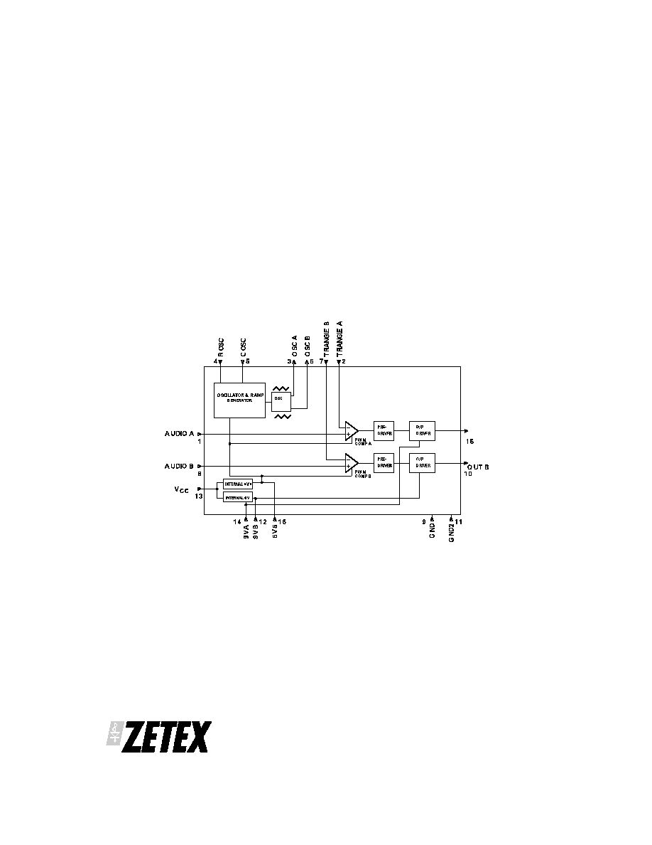
A functional block diagram of the ZXCD1010 is shown
in Figure 2. The on chip series regulators drop the
external V
CC
supply (12V-18V) to the approximate 9V
(9VA/9VB) and 5.5V (5V5) supplies required by the
internal circuitry.
A triangular waveform is generated on chip and is
brought out at the OscA and OscB outputs. The
frequency of this is set (to ~200kHz) by an external
capacitor (C
osc
) and resistor (R
osc
). The triangular
waveform must be externally AC coupled back into the
ZXCD1010 at the TriangleA and TriangleB inputs.
AC coupling ensures symmetrical operation resulting
in minimal system DC offsets. TriangleA is connected
to one of the inputs of a comparator and TriangleB is
connected to one of the inputs of a second comparator.
The other inputs of these two comparators are
connected to the AudioA and AudioB inputs, which are
anti-phase signals externally derived from the audio
input. The triangular wave is an order higher in
frequency than the audio input (max 20kHz). The
outputs of the comparators toggle every time the
TriangleA/B and the (relatively slow) AudioA/B signals
cross.
ZXCD1010
S E M I C O N D U C T O R S
ISSUE 3 - NOVEMBER 2003
4
Out A
Buffers
Figure 2
Functional Block Diagram

With no audio input signal applied, the AudioA/B
inputs are biased at the mid-point of the triangular
wave, and the duty cycle at the output of the
comparators is nominally 50%. As the AudioA/B signal
ascends towards the peak level, the crossing points
with the (higher frequency) triangular wave also
ascend. The comparator monitoring these signals
exhibits a corresponding increase in output duty cycle.
Similarly, as the AudioA/B signal descends, the duty
cycle is correspondingly reduced. Thus the audio input
Pulse Width Modulates the comparator outputs. This
principle is illustrated in Figures 3a, b, c and d. The
comparator outputs are buffered and used to drive the
OutA and OutB outputs. These in turn drive the speaker
load (with the audio information contained in the PWM
signal) via the off chip output bridge and single stage
L-C filter network.
The ramp amplitude is approximately 1V. The AudioA,
AudioB, TriangleA and TriangleB inputs are internally
biased to a DC voltage of approximately VCC/5. The
mid - point DC level of the OscA and OscB triangular
outputs is around 2V. The triangular wave at the Cosc
pin traverses between about 2.7Vand 3.8V and the dist
pin exhibits a roughly square wave from about 1.4V to
2V. (The above voltages may vary in practice and are
included for guidance only).
ZXCD1010
S E M I C O N D U C T O R S
ISSUE 3 - NOVEMBER 2003
5
Audio A/B
Triangle A/B
PWM Comparator
O/P
Audio A/B
Triangle A/B
Comparator O/P
(Duty Cycle = 50%)
O/P
Audio A/B
Triangle A/B
Comparator O/P
(Duty Cycle = 75%)
Audio A/B
Triangle A/B
Comparator O/P
(Duty Cycle = 25%)
Figures 3a,3b,3c and 3d
The audio input Pulse Width Modulates the comparator output