ISSUE 5 - NOVEMBER 2001
ZXCL250 ZXCL260 ZXCL280
ZXCL300 ZXCL330 ZXCL400
1
DESCRIPTION
The ZXCL series are very small low dropout
regulators designed for use in low power and
severely space limited applications.
The devices operate with a low dropout voltage,
typically of only 85mV at 50mA load. Supply current
is minimised with a ground pin current of only 50
µ
A
at full 150mA load. Logic control allows the devices
to be shut down, consuming typically less than 10nA.
These features make the device ideal for battery
powered applications where power economy is
critical.
The parts have been designed with space sensitive
systems in mind. They are available in the ultra small
SC70 package, which is half the size of other SOT23
based regulator devices.
FEATURES
∑
5-pin SC70 package for the ultimate in space
saving
∑
5-pin SOT23 industry standard pinout
∑
Low 85mV dropout at 50mA load
∑
50
µ
A ground pin current with full 150mA load
∑
Typically less than 10nA ground pin current on
shutdown
∑
2.5, 2.6, 2.8, 3, 3.3 and 4 volts output
∑
Very low noise, without bypass capacitor
∑
Thermal overload and over-current protection
∑
-40 to +85∞C operating temperature range
For applications requiring improved performance
over alternative devices, the ZXCL is also offered in
the 5 pin SOT23 package with an industry standard
pinout.
The devices feature thermal overload and
over-current protection and are available with output
voltages of 2.5V, 2.6V, 2.8V, 3V, 3.3V and 4V. Other
voltage options between 1.5V and 4V can be
provided. Contact Zetex marketing for further
information.
The ZXCL series are manufactured using CMOS
processing, however advanced design techniques
mean that output noise is improved even when
compared to other bipolar devices.
APPLICATIONS
∑
Cellular and Cordless phones
∑
Palmtop and laptop computers
∑
PDA
∑
Hand held instruments
∑
Camera, Camcorder, Personal Stereo
∑
PCMCIA cards
∑
Portable and Battery-powered equipment
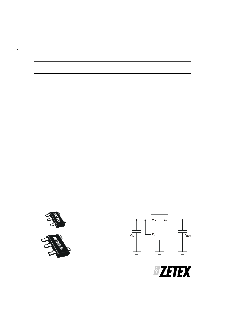
ULTRA SMALL MICROPOWER SC70 LOW DROPOUT REGULATORS
Battery Supply
Output Voltage
ZXCL
TYPICAL APPLICATION CIRCUIT
PACKAGE FOOTPRINT
Total Aea
2.1mm x 2mm
=4.2mm
2
Total Aea
2.8mm x 2.9mm
=8.12mm
2

2
ISSUE 5 - NOVEMBER 2001
ZXCL250 ZXCL260 ZXCL280
ZXCL300 ZXCL330 ZXCL400
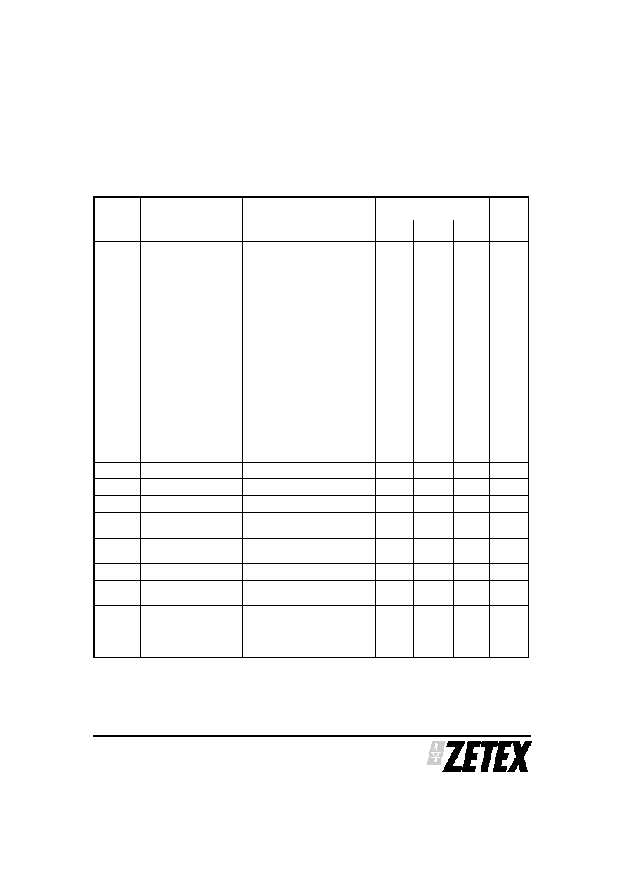
ABSOLUTE MAXIMUM RATINGS
Terminal Voltage with respect to GND
V
IN
-0.3V to 7.0V
E
N
-0.3V to 10V
V
O
-0.3V to 5.5V
Output short circuit duration
Infinite
Continuous Power Dissipation
Internally limited
Operating Temperature Range
-40∞C to +85∞C
Storage Temperature Range
-55∞C to +125∞C
ELECTRICAL CHARACTERISTICS
V
IN
= V
O
+ 0.5V, typical values at TA = 25 C V (Unless otherwise stated)
SYMBOL
PARAMETER
CONDITIONS
LIMITS
UNITS
MIN
TYP
MAX
V
IN
Input Voltage
(note2)
5.5
V
V
O
Output Voltage
I
O
= 1mA
ZXCL250
ZXCL260
ZXCL280
ZXCL300
ZXCL330
ZXCL400
I
O
= 100mA
V
O
+ 0.5V < V
IN
< V
IN
max.
ZXCL250
ZXCL260
ZXCL280
ZXCL300
ZXCL330
ZXCL400
2.450
2.548
2.744
2.940
3.234
3.920
2.425
2.522
2.744
2.910
3.201
3.880
2.5
2.6
2.8
3.0
3.3
4.0
2.550
2.652
2.856
3.060
3.366
4.080
2.575
2.678
2.884
3.090
3.399
4.120
V
V
V
O
/
T
Output Voltage
Temperature
Coefficient
-15
ppm/∞C
I
O(MAX)
Output Current
ZXCL250 only
150
100
mA
I
OLIM
Over Current Limit
ZXCL250 only
160
105
230
800
750
mA
I
Q
Ground pin current
No Load
I
O
= 150mA,
I
O
= 100mA,
25
50
40
50
120
100
A
A
A
Stresses beyond those listed under "Absolute Maximum Ratings" may cause permanent damage to the
device. These are stress ratings only, and functional operation of the device at these or any other conditions
beyond those indicated in the operational sections of the specifications is not implied. Exposure to absolute
maximum conditions for extended periods may affect device reliability.
Package Power Dissipation (T
A
=25∞C)
SC70
300mW (Note 1)
SOT23-5
450mW (Note 1)
ELECTRICAL CHARACTERISTICS
V
IN
= V
O
+ 0.5V, typical values at T
A
=25∞C (Unless otherwise stated)
ZXCL250 ZXCL260 ZXCL280
ZXCL300 ZXCL330 ZXCL400
ISSUE 5 - NOVEMBER 2001
3
SYMBOL
PARAMETER
CONDITIONS
LIMITS
UNITS
MIN
TYP
MAX
V
DO
Dropout Voltage
Note 3
ZXCL250
I
O
=10mA
I
O
=50mA
I
O
=100mA
ZXCL260
I
O
=10mA
I
O
=50mA
I
O
=100mA
ZXCL280
I
O
=10mA
I
O
=50mA
I
O
=100mA
ZXCL300
I
O
=10mA
I
O
=50mA
I
O
=100mA
ZXCL330
I
O
=10mA
I
O
=50mA
I
O
=100mA
ZXCL400
I
O
=10mA
I
O
=50mA
I
O
=100mA
15
85
163
15
85
155
15
85
140
15
85
140
15
85
140
15
85
140
325
310
280
280
280
280
mV
mV
mV
mV
mV
mV
V
LNR
Line Regulation
V
IN
=(V
O
+0.5V) to 5.5V, I
O
=1mA
0.02
0.1
%/V
V
LDR
Load Regulation
I
O
=1mA to 100mA
0.01
0.04
%/mA
E
N
Output Noise Voltage
f=10Hz to 100kHz, C
O
=10
µ
F,
50
µ
V rms
V
ENH
Enable pin voltage for
normal operation
T
A
= -40
∞
C
2
2.2
10
V
V
ENL
Enable pin voltage for
output shutdown
0
0.8
V
V
ENHS
Enable pin hysteresis
150
mV
I
EN
Enable Pin input
current
V
EN
=5.5V
100
nA
I
QSD
Shutdown supply
current
V
EN
=0V
1
µ
A
T
SD
Thermal Shutdown
Temperature
125
165
∞C
Device testing is performed at T
A
=25 C. Device thermal performance is guaranteed by design.
Note1: Maximum power dissipation is calculated assuming the device is mounted on a PCB measuring 2
inches square
Note 2: Output Voltage will start to rise when V
IN
exceeds a value or approximately 1.3V. For normal
operation, V
IN
(min) > V
OUT
(nom) + 0.5V.
Note 3: Dropout voltage is defined as the difference between V
IN
and V
O
, when V
O
has dropped 100mV below
4
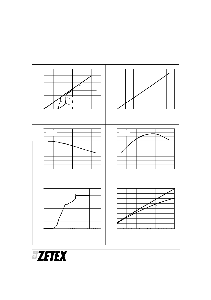
-50
-25
0
25
50
75
100
2.79
2.80
2.81
-50
-25
0
25
50
75
100
23.0
23.2
23.4
23.6
23.8
24.0
24.2
24.4
24.6
24.8
25.0
0
1
2
3
4
5
0
5
10
15
20
25
30
0
25
50
75
100
125
150
20
25
30
35
40
45
50
55
60
0
1
2
3
4
5
6
0
1
2
3
4
5
6
0
25
50
75
100
125
150
175
0.00
0.05
0.10
0.15
0.20
0.25
V
IN
= 3.3V
No Load
Output Voltage v Temperature
Output
Voltage
(V)
Temperature (∞C)
V
IN
= 3.3V
No Load
Ground Current v Temperature
Gr
ound
Cur
r
ent
(µA)
Temperature (∞C)
No Load
Ground Current v Input Voltage
Gr
ound
Cur
r
ent
(µA)
Input Voltage (V)
V
IN
= 3.3V
V
IN
= 5V
Ground Current v Load Current
Gr
ound
Cur
r
ent
(µA)
Load Current (mA)
V
IN
I
OUT
= 100mA
I
OUT
= 1mA
Input to Output Characteristics
Volt
age
(V
)
Input Voltage (V)
Dropout Voltage v Output Current
D
r
opout
Voltage
(V)
Output Current (mA)
ISSUE 5 - NOVEMBER 2001
ZXCL250 ZXCL260 ZXCL280
ZXCL300 ZXCL330 ZXCL400
TYPICAL CHARACTERISTICS
(ZXCL280 shown)
ISSUE 5 - NOVEMBER 2001
ZXCL250 ZXCL260 ZXCL280
ZXCL300 ZXCL330 ZXCL400
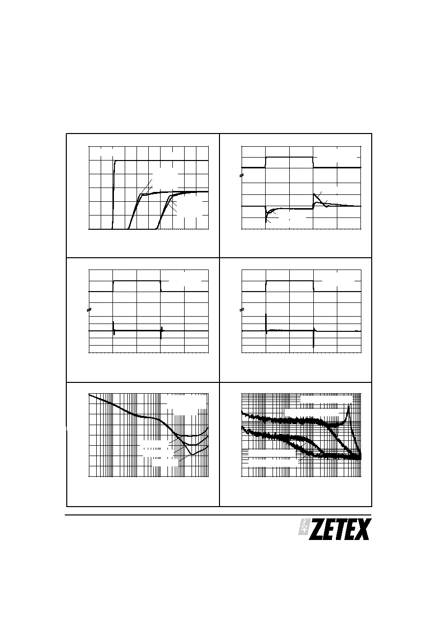
5
0.0
0.1
0.2
0.3
0.4
0.5
-20
-10
0
10
20
3
4
5
6
0
10
20
30
40
50
60
70
80
90
100
0
1
2
3
4
5
6
0.0
0.1
0.2
0.3
0.4
0.5
-20
-10
0
10
20
3
4
5
6
0.0
0.1
0.2
0.3
0.4
0.5
-100
-50
0
50
100
0
50
100
10
100
1k
10k
100k
1M
0.01
0.1
1
10
10
100
1k
10k
100k
1M
0
10
20
30
40
50
60
70
80
C
OUT
= 1
mF
T
r
& T
f
= 2.5
ms
Line Rejection I
L
= 100mA
D
V
OUT
(mV)
V
IN
(V)
Time (ms)
V
IN
= 5V
I
L
= 1mA
I
L
= 100mA
Enable
V
IN
= 3.3V
I
L
= 1mA
I
L
= 100mA
C
OUT
= 1
mF
Start-Up Response
Voltage
(V)
Time (
µ
s)
C
OUT
= 1
mF
T
r
& T
f
= 2.5
ms
D
V
OUT
(mV)
V
IN
(V)
Line Rejection I
L
= 1mA
Time (ms)
C
OUT
= 10
mF
C
OUT
= 1
mF
C
OUT
= 10
mF
C
OUT
= 1
mF
V
IN
= 5V
I
L
= 1mA to 50mA
Load Response
D
V
OUT
(mV)
I
L
(mA)
Time (ms)
I
L
= 100mA, C
OUT
= 1
mF
I
L
= 100mA, C
OUT
= 10
mF
No Load, C
OUT
= 10
mF
No Load, C
OUT
= 1
mF
Output Noise v Frequency
Noise
µ
V/
Hz
Frequency (Hz)
All Caps Ceramic
Surface Mount
I
L
= 50mA
C
OUT
= 1
mF
C
OUT
= 2.2
mF
C
OUT
= 10
mF
Power Supply Rejection v Frequency
Power
Supply
Rejection
(dB)
Frequency (Hz)
TYPICAL CHARACTERISTICS
(ZXCL280 shown)