 | –≠–ª–µ–∫—Ç—Ä–æ–Ω–Ω—ã–π –∫–æ–º–ø–æ–Ω–µ–Ω—Ç: ZXCM209XF | –°–∫–∞—á–∞—Ç—å:  PDF PDF  ZIP ZIP |

ISSUE 3 - FEBRUARY 2001
ZXCM209
ZXCM210
DESCRIPTION
The ZXCM209/210 are three terminal supervisory
circuits used to monitor the power supplies in
microprocessor and digital systems. They provide a
high performance economical solution when used
with 5V, 3V or lower powered circuits. Reset
thresholds suitable for operation with a variety of
supply voltages are available.
These devices provide a reset signal whenever the
supply voltage falls below a preset threshold, keeping
it asserted for a minimum delay period of 140ms after
the supply has risen above the reset level. The
ZXCM209 has an active-low RESET output (which is
guaranteed to be in the correct state for supplies down
to 1V), while the ZXCM210 has an active-high RESET
output.
The reset comparator has in built hysteresis to prevent
erratic operation and is designed to ignore supply
transients. Low supply current (typically 2µA) makes
the ZXCM209/210 devices ideal for use in portable
equipment. They are available in a 3-pin SOT23
surface mount package with an industry standard
pinout.
FEATURES
∑
Enhanced alternative to MAX809/810 and similar
parts
∑
Precision monitoring of 5V, 3.3V, 3V power
supply voltages
∑
1% threshold tolerance
∑
2µA typical supply current
∑
140ms minimum power on reset pulse width
∑
Alternative minimum pulse widths available,
contact your local sales office for availability
∑
RESET LOW Output (ZXCM209)
∑
RESET HIGH Output (ZXCM210)
∑
Power supply transient immunity
∑
No latch up
∑
No external components
∑
3-Pin SOT23 package
APPLICATIONS
∑
Computer systems
∑
Controllers
∑
Instrumentation
∑
Microprocessor power monitoring
∑
Microcontroller power monitoring
∑
Power supplies
∑
Portable/Battery-powered equipment
∑
Automotive
VERY LOW POWER MICROPROCESSOR RESET DEVICES
APPLICATION CIRCUIT
v
cc
ZXCM
Reset
Output
Gnd
v
cc
v
cc
Micro
Reset
Input
Gnd
1
ZXCM209
ZXCM210
ABSOLUTE MAXIMUM RATINGS
Terminal Voltage with respect to G
ND
V
CC
-0.3V to 7.0V
RESET, RESET
-0.3V to (V
CC
+ 0.3V)
Input Current, V
CC
20mA
Output Current
20mA
Rate of Rise, V
CC
250V/µs
Continuous Power Dissipation
500mW
Operating Temperature Range
-55∞C to +125∞C
Storage Temperature Range
-65∞C to +150∞C
Stresses beyond those listed under "Absolute Maximum Ratings" may cause permanent damage to the device.
These are stress ratings only, and functional operation of the device at these or any other conditions beyond
those indicated in the operational sections of the specifications is not implied. Exposure to absolute maximum
conditions for extended periods may affect device reliability.
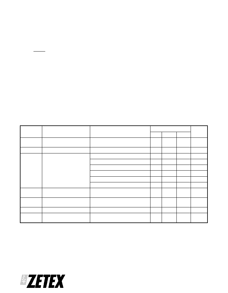
ELECTRICAL CHARACTERISTICS
TEST CONDITIONS (unless otherwise stated) V
CC
= full range, T
A
= -55∞C to +125∞C
SYMBOL
PARAMETER
CONDITIONS
LIMITS
UNITS
MIN
TYP
MAX
V
R
V
CC
Range
T
A
=0∞ to 70∞C
T
A
=-55∞ to 125∞C
1.0
1.2
5.5
5.5
V
V
I
CC
Supply Current
2
5
µ
A
V
TH
Reset Threshold
Suffix L; T
A
=25∞C
4.58
4.63
4.68
V
Suffix M; T
A
=25∞C
4.34
4.38
4.42
V
Suffix J; T
A
=25∞C
3.96
4.00
4.04
V
Suffix T; T
A
=25∞C
3.05
3.08
3.11
V
Suffix S; T
A
=25∞C
2.90
2.93
2.96
V
Suffix R; T
A
=25∞C
2.60
2.63
2.66
V
V
THT
Reset Threshold
Tolerance
T
A
=25∞C
T
A
=-55∞ to 125∞C
1
5
%
%
V
TH
/∞C
Reset Threshold Temp.
Coefficient
50
ppm/∞C
V
D
V
CC
to Reset Delay
30
µ
s
V
TO
Reset Active Timeout
Period
140
560
ms
2
2
ISSUE 3 - FEBUARY 2001
ISSUE 3 - FEBRUARY 2001
ZXCM209
ZXCM210
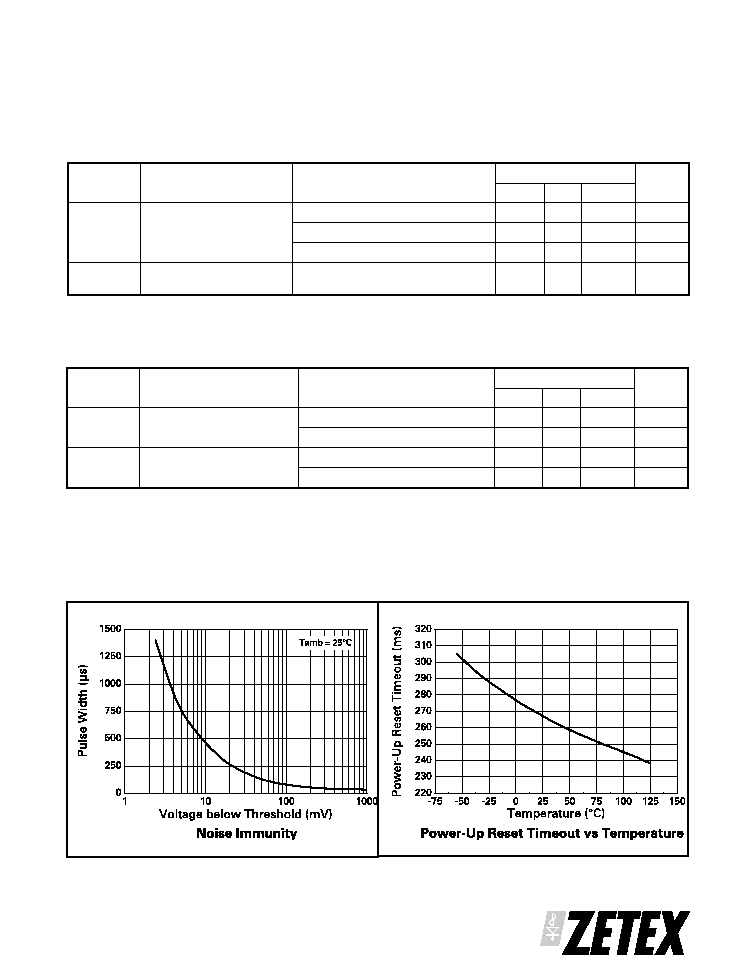
ELECTRICAL CHARACTERISTICS ZXCM209
TEST CONDITIONS (unless otherwise stated) V
CC
= full range, T
A
= -55∞C to +125∞C
SYMBOL
PARAMETER
CONDITIONS
LIMITS
UNITS
MIN
TYP
MAX
V
OL
Reset Output Voltage
Low
V
CC
>1V, I
OL
=100µA (0 to 85∞C)
0.3
V
V
CC
>1.2V, I
OL
=200µA
0.3
V
V
TH
>V
CC
>2.5V, I
OL
=2.7mA
0.4
V
V
OH
Reset Output Voltage
High
V
CC
>V
TH
max, I
OH
=1mA
0.8V
cc
V
ELECTRICAL CHARACTERISTICS ZXCM210
TEST CONDITIONS (unless otherwise stated) V
CC
= full range, T
A
= -55∞C to +125∞C
SYMBOL
PARAMETER
CONDITIONS
LIMITS
UNITS
MIN
TYP
MAX
V
OL
Reset Output Voltage
Low
V
CC
>V
TH
max, I
OL
=2mA
0.3
V
V
CC
>V
TH
max, I
OL
=2.7mA
0.4
V
V
OH
Reset Output Voltage
High
V
CC
>1.5V, I
OH
=150µA
0.8V
cc
V
V
CC
>V
TH
>2.5V, I
OH
=1mA
0.8V
cc
V
Note: Device testing is performed at T
A
=25∞C. Device thermal performance is guaranteed by design
TYPICAL CHARACTERISTICS
3

ZXCM209
ZXCM210
ISSUE 3 - FEBUARY 2001
TYPICAL CHARACTERISTICS
4
ISSUE 3 - FEBRUARY 2001
ZXCM209
ZXCM210
APPLICATIONS INFORMATION
Negative going V
CC
transients
The ZXCM209/210 are, to a good degree, immune to
short duration negative going supply transients. Under
certain circumstances very brief transients are allowed
without inappropriate false triggering of the reset
circuit. The response to supply transients is shown in the
Noise Immunity graph in the typical characteristics. The
graph indicates the typical allowable transient duration
for a specified threshold overdrive such that a reset
pulse is not generated. Addition of a bypass capacitor,
e.g. 0.1µF, as close as possible to the V
CC
pin will provide
extra transient immunity.
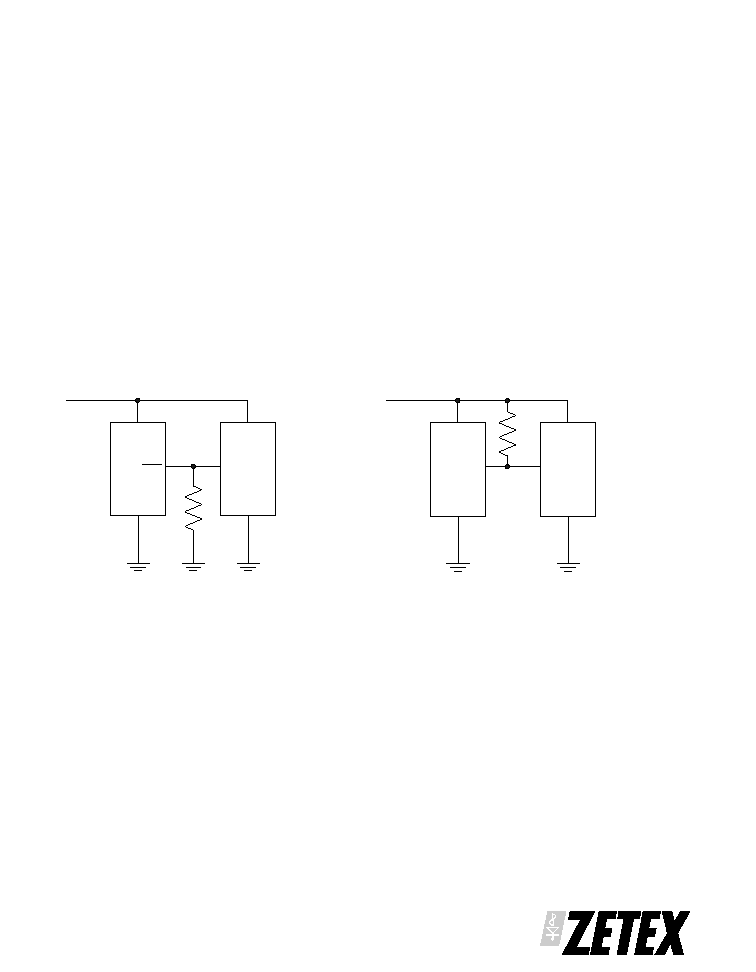
Reset valid down to very low supply voltages
With V
CC
between 0V and 1V the output of the
ZXCM209/210 may be in an undefined state. In many
s y s t e m s
t h i s
i s
i n c o n s e q u e n t i a l
a s
t h e
microprocessor, and other circuits, will be inoperative
with supplies this low. In applications where this is
important, the addition of an external resistor ensures
that the reset output remains valid for V
CC
< 1V. The
resistor value is non critical: a value of 100k
is
recommended. For the ZXCM209 the resistor should
be applied between reset output and ground: for the
ZXCM210 between reset output and V
CC
. Figure 1
shows the connection diagram for the ZXCM devices
in these configurations.
v
cc
ZXCM210
Reset
Output
Gnd
v
cc
Micro
Reset
Input
Gnd
v
cc
100k
v
cc
ZXCM209
Reset
Output
Gnd
v
cc
Micro
Reset
Input
Gnd
v
cc
100k
Figure 1
Circuit for operation of ZXCM with reset valid down to very low supply voltage.
5