
S E M I C O N D U C T O R S
DESCRIPTION
The ZXCT1022 is a precision high side current sense
monitor. Using this type of device eliminates the need
to disrupt the ground plane when sensing a load
current.
The ZXCT1022 provides a fixed gain of 100 for
applications where minimal sense voltage is required.
The very low offset voltage enables a typical accuracy
of 3% for sense voltages of only 10mV, giving better
tolerances for small sense resistors necessary at
higher currents.
The wide input voltage range of 20V down to as low as
2.5V make it suitable for a range of applications. With a
minimum operating current of just 25µA, combined
with its SOT23-5 package make it suitable for portable
battery equipment too.
FEATURES
∑
Accurate high-side current sensing
∑
Output voltage scaling
∑
2.5V ≠ 20V supply range
∑
25 A quiescent current
∑
1% typical accuracy
∑
SOT23-5 package
APPLICATIONS
∑
Battery chargers
∑
Smart battery packs
∑
DC motor control
∑
Over current monitor
∑
Power management
∑
Level translating
∑
Programmable current source
ZXCT1022
PROVISIONAL ISSUE J - APRIL 2004
LOW OFFSET HIGH-SIDE CURRENT MONITOR
1
DEVICE
REEL
SIZE
TAPE
WIDTH
QUANTITY PER
REEL
ZXCT1022E5TA
7"
8mm
3,000 units
DEVICE MARKING
1022
ORDERING INFORMATION
TYPICAL CIRCUIT APPLICATION

Absolute Maximum Ratings
Voltage on any pin
-0.6V to 20V
V
sense
-0.6V to Vin + 0.5V
Operating temperature
-40 to 85
∞C
Storage temperature
-55 to 150
∞C
Package power dissipation
(T
A
= 25
∞C)
SOT23
450mW
ZXCT1022
S E M I C O N D U C T O R S
PROVISIONAL ISSUE J - APRIL 2004
2
SYMBOL
PARAMETER
CONDITIONS
LIMITS
UNIT
Min
Typ
Max
V
in
V
CC
range
2.5
20
V
V
out
Output voltage
(ZXCT1022)
V
sense
= 0V
V
sense
= 10mV
V
sense
= 30mV
V
sense
= 100mV
0
0.97
2.91
9.7
30
1.0
3.0
10.0
100
1.03
3.09
10.3
mV
V
V
V
R
out
Output resistance
10
15
20
K
T
c
Output temperature
coefficient
50
300
ppm
I
q
Ground pin current
V
sense
= 0V
25
35
A
V
sense
(2)
Sense voltage
0
1.5
V
I
sense
Load pin input
current
100
nA
Acc
Accuracy
V
sense
= 10mV
-3
3
%
Gain
V
out
/ V
sense
V
sense
= 10mV
0.97
1.0
1.03
V
BW
Bandwidth
V
sense
= 10mV
V
sense
= 100mV
300
2
kHz
MHz
ELECTRICAL CHARACTERISTICS Test Conditions T
A
= 25
∞C, V
in
= 15V
NOTES
(2)
Vsense= Vin - Vload
T
C
Limits are determined by characterization.

TYPICAL CHARACTERISTICS
ZXCT1022
S E M I C O N D U C T O R S
PROVISIONAL ISSUE J - APRIL 2004
3

TYPICAL CHARACTERISTICS
ZXCT1022
S E M I C O N D U C T O R S
PROVISIONAL ISSUE J - APRIL 2004
4
BLOCK DIAGRAM
Application information
The ZXCT1022 has a fixed dc voltage gain of 100. No external scaling resistors are required for the output. Output
voltage is simply defined as:
Where V
sense
= V
in
- V
Load
PCB trace shunt resistor for low cost solution
The figure below shows a PCB layout suggestion for a low cost solution where a PCB resistive trace in
replacement for a conventional shunt resistor, can be used. The resistor section is 25mm x 0.25mm giving
approximately 150m
using 1 oz copper. Smaller resistances can be used if required.
Total circuit solution: 1 component. Shows area of 150m
sense resistor
compared to SOT23 package.
Practical tolerance of the PCB resistor will be around 5% depending on
manufacturing methods.
ZXCT1022
S E M I C O N D U C T O R S
PROVISIONAL ISSUE J - APRIL 2004
5
V
out
= 100 x V
sense
(V)
GND
Load
Top view
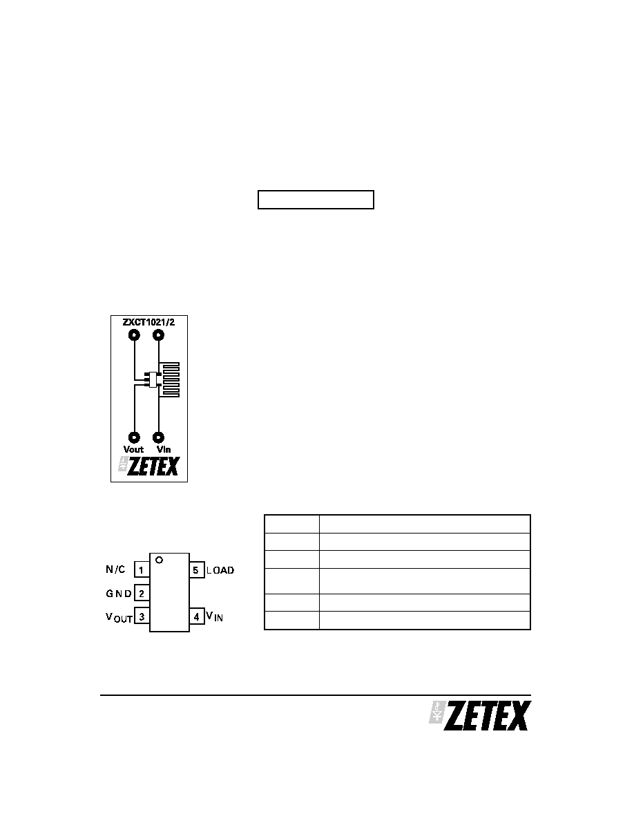
PINOUT
PIN NAME
PIN FUNCTION
N/C
Not internally connected
GND
Ground
V
out
Voltage output referenced to GND. Intended to
drive high impedance loads
Load
High impedance negative sense voltage input
V
in
Supply and positive sense voltage input