
S E M I C O N D U C T O R S
DESCRIPTION
The ZXCT1030 is a high side current sense monitor
containing an internal reference and comparator with a
non-latching output. Using this device eliminates the
need to disrupt the ground plane when sensing a load
current.
The wide input voltage range of 20V down to as low as
2.2V make it suitable for a range of applications.
Dynamics and supply current are optimised for the
processing of fast pulses, associated with switch mode
applications.
FEATURES
∑
Low cost, accurate high-side current sensing.
∑
Output voltage scaling.
∑
Up to 18V output.
∑
2.2V ≠ 20V supply range.
∑
270 A quiescent current.
∑
1.5% typical accuracy.
∑
MSOP8 Package.
∑
Voltage reference on chip
∑
Comparator on chip
DEVICE MARKING
∑
ZXCT
1030
APPLICATIONS
∑
Battery chargers
∑
Electronic fuse
∑
DC motor control
∑
Over current monitor
∑
Power management
∑
Inrush current limiting
ZXCT1030
PROVISIONAL ISSUE J - MAY 2004
HIGH-SIDE CURRENT MONITOR WITH COMPARATOR
1
+
-
Comp_in
Vout
Comp_out
To load
Rsense
Vin
sense+
sense-
Current
Monitor
Rcomp
5V Vcomp_supply
ZXCT1030
Vcc
Vref_out
FUNCTIONAL BLOCK DIAGRAM
ORDERING INFORMATION
Device
Reel size
Tape width
Quantity per reel
ZXCT1030X8TA
7"
12mm
500 units
ZXCT1030X8TC
13"
12mm
2500 units
Absolute Maximum Ratings
Voltage on any pin
-0.6V and V
cc
+0.6V
Operating Temperature
-40 to 85
∞C
Storage Temperature
-55 to 125
∞C
Package Power Dissipation
(T
A
= 25
∞C)
MSOP8
500mW
ZXCT1030
S E M I C O N D U C T O R S
PROVISIONAL ISSUE J - MAY 2004
2
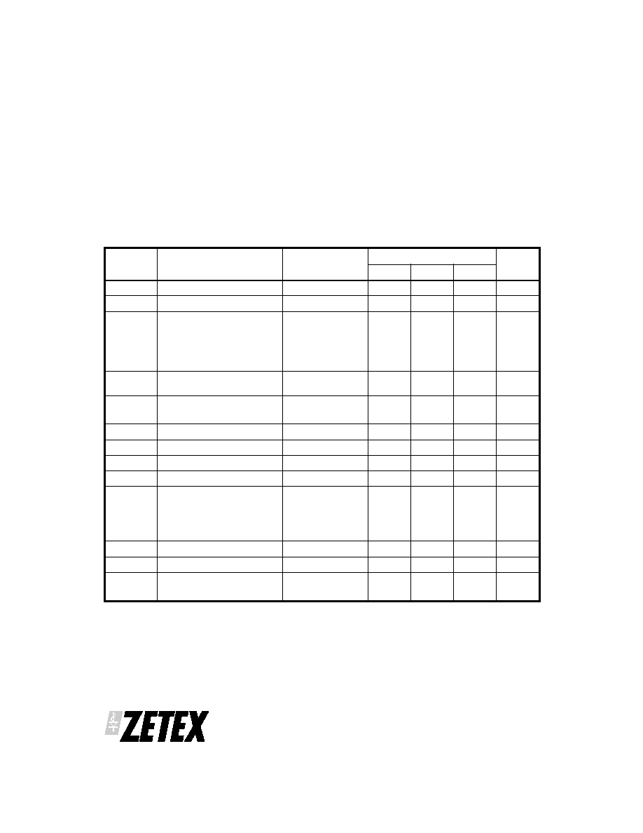
SYMBOL
PARAMETER
CONDITIONS
LIMITS
UNIT
Min
Typ
Max
V
CC
V
CC
Range
2.2
20
V
V
sense+
Sense+ range
2.2
V
CC
V
out
Output Voltage
V
sense
= 0V
V
sense
= 10mV
V
sense
= 30mV
V
sense
= 50mV
V
sense
= 100mV
V
sense
= 500mV
0
88
284
480
970
4500
2
100
300
500
1000
5000
10
112
316
520
1030
5500
mV
mV
mV
mV
mV
mV
R
out
Output resistance
V
sense-
= 15V,
V
out
= 1V
1.2
1.5
1.8
K
V
out
TC
V
out
temperature coefficient
30
ppm/ C
I
CC
Supply current
V
sense-
= 15V
170
270
350
µA
I
sense+
Sense+ input current
25
48
90
µA
I
sense-
Sense- input current
V
sense-
= 14.9V
25
70
220
nA
V
sense
2
Sense Voltage
0
500
mV
V
cm
3
Common Mode Range
V
cc
= 15V
V
comp_supply
= 5V
V
comp_in
= V
ref
V
sense
= 10mV
2.8
V
Acc
Accuracy
V
sense
= 100mV
-3
3
%
Gain
V
out
/ V
sense
V
sense
= 100mV
9.7
10.0
10.3
BW
Bandwidth
V
sense
= 10mVp-p
V
sense
= 100mVp-p
3
6
MHz
MHz
ELECTRICAL CHARACTERISTICS Test Conditions T
A
= 25
∞C, V
in
= V
cc
= 15V
2
Vsense = (Vsense +) - (Vsense -)
3
Level of Vin where comparator output defaults to `off'.

Absolute Maximum Ratings
Voltage on any pin
-0.6V and V
cc
+0.6 V
Operating Temperature
-40 to 85
∞C
Storage Temperature
-55 to 125
∞C
Package Power Dissipation
(T
A
= 25
∞C)
MSOP8
500mW
ZXCT1030
S E M I C O N D U C T O R S
PROVISIONAL ISSUE J - MAY 2004
3
SYMBOL
PARAMETER
CONDITIONS
LIMITS
UNIT
Min
Typ
Max
Comparator
Vcomp
Input Voltage
0.005
10
V
V
H
Hysteresis
V
comp_supply
= 5V
R
comp
= 10k
15
mV
I
B
Input Bias
V
comp_supply
= 5V
V
comp- in
= 1V
R
comp
= 10k
5
50
100
nA
T
D
Propagation Delay
V
comp_supply
= 5V
R
comp
= 10k
100
ns
V
OL
Output Voltage Low
V
comp_supply
= 5V
R
comp
= 10k
30
150
200
mV
V
OH
Output Voltage High
V
comp_supply
= 5V
R
comp
= 10k
V
comp_
supply
V
I
OL
Output Sink Current
V
OL
= 0.4V
2
mA
I
OH
Output High Leakage
Current
V
comp_supply
= 5V
R
comp
= 10K
1.0
µA
Voltage Reference
V
ref
Reference Current
= 0 A
Reference Current
= -300 A
Reference Current
= +5 A
1.200
1.200
1.200
1.240
1.240
1.240
1.280
1.280
1.280
V
V
V
delta V
ref
Change in Vref
Isource 5 A to
Isink 300 A
10
mV
TC
30
ppm/ C
PSR
Supply rejection
0.01
%/V
ELECTRICAL CHARACTERISTICS (Cont.) Test Conditions T
A
= 25
∞C, V
in
= Vcc = 15V
ZXCT1030
S E M I C O N D U C T O R S
PROVISIONAL ISSUE J - MAY 2004
4
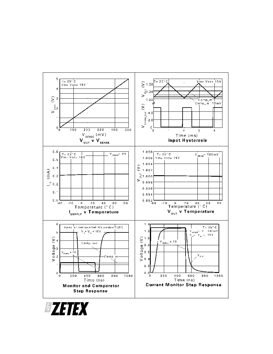
TYPICAL CHARACTERISTICS
Voltage output Current Monitor
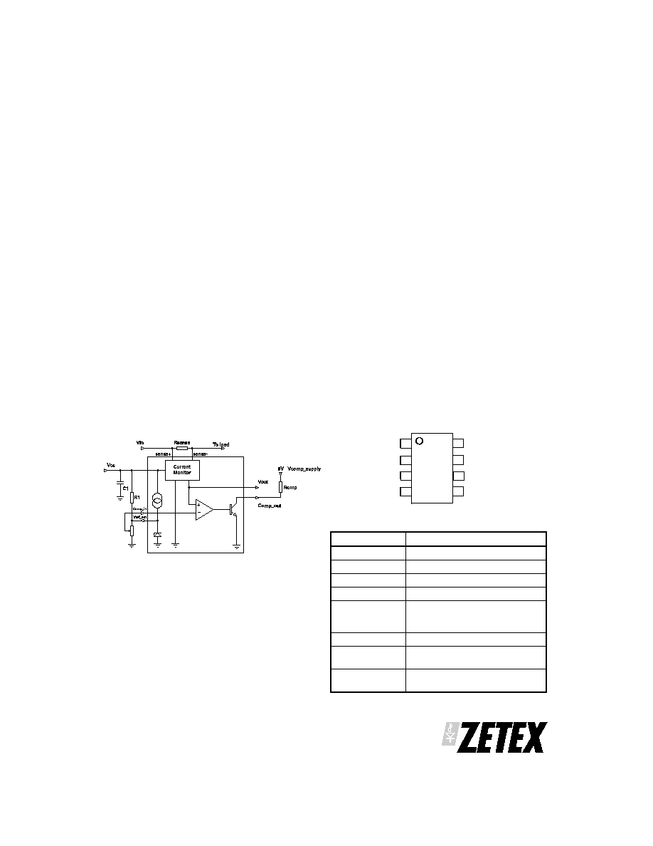
Referring to the block diagram, the current monitor
takes the small voltage developed across the sense
resistor (Vsense) and transfers it from the large
common mode supply voltage to a ground-referenced
signal with a gain of 10. The sense input common
mode range is 2.2V to 20V. In this range, a linear output
voltage is delivered.
Reference
The bandgap reference allows the comparator to
compare the translated Vsense with threshold value
chosen by the user which can be any voltage from 0 to
1.24V, configured by two external resistors which
forms Vcomp_in.
The output current which can be drawn from the
comparator reference (I
ref
source) is limited to 5
µA,
making potentiometers
250k suitable for setting a
threshold level. Where a lower potentiometer resistor
value is used, an additional resistor value should be
inserted between V
ref
and V
cc
to maintain sufficient
current for the reference. (as shown in figure 1.0).
The Voltage reference has a maximum current sink
capability. This magnitude of current will be influenced
by the value of R
1
which is inserted between V
ref
and
V
cc.
The value of current flowing through R
1
can be
expressed as:
I = (Vcc -Vref) / R
1
Comparator
The open collector output is active low and is asserted
when Vsense x 10 (Vout) > Vcomp_in.
It can be connected to any voltage rail up to Vin via a
pull-up resistor. Suggest values for the resistor are in
the range of 10-100k .
In the case where high load currents or a short circuit
occurs, thus reducing the common mode signals (V+,
V-) typically below 2.2V, the comparator will default to
the asserted state. This can eliminate a closed loop
system `latch-up' condition, allowing the controller to
remove the applied power.
Stability
To ensure stable operation of the ZXCT1030, it is
recommended a decoupling capacitor is placed across
the V
CC
and ground connections. A ceramic 10 F will
be adequate.
Pin Name
Pin Function
Vcc
Supply voltage
Sense-
Negative sense input
Sense+
Positive sense input
GND
Ground
Comp_in
Comparator input, usually a
ratio of the reference or other
control signal.
Vref_out
Reference output
Vout
Current Monitor output
voltage
Comp_out
Open collector comparator
output
ZXCT1030
S E M I C O N D U C T O R S
PROVISIONAL ISSUE J - MAY 2004
5
Vcc
Sense-
Sense+
GND
Comp_out
Vout
Vref_out
Comp_in
1
2
3
4
8
7
6
5
PIN CONNECTIONS
MSOP8
FIGURE 1.0
External resistor for reference level

ZXCT1030
S E M I C O N D U C T O R S
6
PROVISIONAL ISSUE J - MAY 2004
Europe
Zetex GmbH
Streitfeldstraþe 19
D-81673 M¸nchen
Germany
Telefon: (49) 89 45 49 49 0
Fax: (49) 89 45 49 49 49
europe.sales@zetex.com
Americas
Zetex Inc
700 Veterans Memorial Hwy
Hauppauge, NY 11788
USA
Telephone: (1) 631 360 2222
Fax: (1) 631 360 8222
usa.sales@zetex.com
Asia Pacific
Zetex (Asia) Ltd
3701-04 Metroplaza Tower 1
Hing Fong Road, Kwai Fong
Hong Kong
Telephone: (852) 26100 611
Fax: (852) 24250 494
asia.sales@zetex.com
Corporate Headquaters
Zetex Semiconductors plc
Zetex Technology Park, Chadderton
Oldham, OL9 9LL
United Kingdom
Telephone (44) 161 622 4444
Fax: (44) 161 622 4446
hq@zetex.com
These offices are supported by agents and distributors in major countries world-wide.
This publication is issued to provide outline information only which (unless agreed by the Company in writing) may not be used, applied or reproduced
for any purpose or form part of any order or contract or be regarded as a representation relating to the products or services concerned. The Company
reserves the right to alter without notice the specification, design, price or conditions of supply of any product or service.
For the latest product information, log on to www.zetex.com
© Zetex Semiconductors plc 2004
H
E
D
e X 6
A
A
1
L
C
1
2
3
4
5
6
7
8
B
PACKAGE DIMENSIONS
PAD LAYOUT DETAILS
DIM
Millimetres
Inches
MIN
MAX
MIN
MAX
A
-
1.10
-
0.043
A1
0.05
0.15
0.002
0.006
B
0.25
0.40
0.010
0.016
C
0.13
0.23
0.005
0.009
D
2.90
3.10
0.114
0.122
e
0.65 BSC
0.0256 BSC
E
2.90
3.10
0.114
0.122
H
4.90 BSC
0.193 BSC
L
0.40
0.70
0.016
0.028
∞
0∞
6∞
0∞
6∞
PACKAGE DIMENSIONS