
DESCRIPTION
The ZXF103 is a versatile analog high Q bandpass filter.
It can be configured to provide pass or notch
characteristics.
The basic filter section requires 2 resistors and 2 capacitors to set the centre frequency. The frequency range is up
to 600kHz. Two external resistors control filter Q Factor. The Q can be varied up to 50.
APPLICATIONS
Many filter applications including: -
∑
Sonar and Ultrasonic Systems
∑
Line frequency notch
∑
Signalling
∑
Motion detection
∑
Instrumentation
∑
Low frequency telemetry
FEATURES AND BENEFITS
∑
Centre Frequency up to 1MHz
∑
Variable Q up to 50
∑
Low distortion
∑
Low noise
∑
Low power 25mW
∑
Devices easily cascaded
∑
Small QSOP16 package
ZXF103
ISSUE 1 - APRIL 2002
VARIABLE Q FILTER
1
R
R
C
C
R
Q SET
ZXF103
Filter Input
Filter Output
SYSTEM DIAGRAM
PART NUMBER
PACKAGE
PART
MARK
ZXF103Q16
QSOP16
ZXF103
ORDERING INFORMATION
PART NUMBER
CONTAINER
INCREMENT
ZXF103Q16TA
Reel 7"
178mm
500
ZXF103Q16TC
Reel 13"
330mm
2500
R2
0V
RC2
GP1
Vcc
GP3
BIAS
RC1
0V
C1
FI1
GP2
NC
Vcc
FO
FI2
1
16
PINOUT

ZXF103
ISSUE 1 - APRIL 2002
2
ABSOLUTE MAXIMUM RATINGS
Voltage on any pin
7.0V (relative to 0V)
Operating temperature range
0 to 70∞C
Storage temperature
-55 to 125∞C
ELECTRICAL CHARACTERISTICS
Test Co
ditions: Temperature =25∞C, V
CC
= 5.00V, 0V =0.00V,
R
L
=10k,C
L
=10pF
GENERAL CHARACTERISTICS
Parameter
Conditions
Min.
Typical
Max.
Units
Operating current
4.0
5.0
mA
Max. operating frequency
Vout=1.6V p-p
Vout=1.0V p-p
600
1000
kHz
Q usable range
0.5
50
Centre Frequency temperature
coefficient
Q=30,
fo = 1kHz
100
ppm/∞C
Q temperature coefficient
Q=30,
fo = 1kHz
0.1
% /∞C
Voltage noise
1 ≠ 100 kHz
20
nV/
Hz
Input impedance
10
15
20
k
Linear Output Range
Output load
=
10 k
2
V pk-pk
Sink current
450
µ
A
Source current
450
µ
A
Pin
Name
Function
1
R2
Phase retard node
2
0V
0 Volts
3
RC2
Phase retard node
4
BIAS
Internal bias generator
5
RC1
Phase advance node
6
0V
0 Volts
7
C1
Phase advance node
8
FI1
Filter input mode dependent
9
FI2
Filter input, mode dependent
10
FO
Filter output for all modes
11
Vcc
+5 Volt supply
12
N/C
No connection
13
GP2
Loop gain node
14
GP3
Loop gain node
15
Vcc
+5 Volt supply
16
GP1
Loop gain node
11.78
11.79
11.80
11.81
11.82
Number
o
f
Devi
ces
Frequency (KHz)
Histogram of Centre Frequency
(Fo = 11.80KHz Q = 25)
ZXF103
ISSUE 1 - APRIL 2002
5
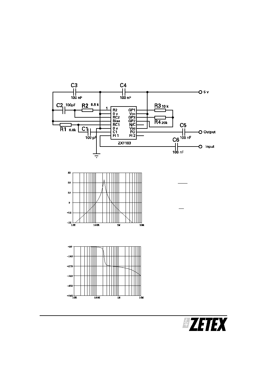
Filter Configurations and Responses (Continued)
Inverse Notch Filter (with attenuating skirts)
10K
100K
1M
10M
-20
-10
0
10
20
30
Frequency (Hz)
Gain
(dB)
AC Filter Performance
10K
100K
1M
10M
-540
-450
-360
-270
-180
-90
Frequency (Hz)
Phase
(
deg)
Fo
1
2 RC
=
where R=R1=R2
and
C=C1=C2
Q
R4
R3
where R1,R2,R3 and R4
2k
and C1 and C2
50pF
See "Designing for a value of Q"
for more details.
The skirt `roll off' away from the
peak is -20dB/Decade regardless
of chosed Q.
Typical responses from the
circuit with component values
derived from the diagram.

