TARGET - FEB 2001
ZXFV202
DEVICE DESCRIPTION
The ZXFV202 is a single high speed amplifier designed
for video and other high speed applications. Packaged
in a small SOT23-5 it is ideally suited to applications
where space is at a premium. In applications where
cross talk is critical this part provides better isolation
than dual or quad devices.
I t f e a t u r e s l o w d i f f e r e n t i a l g a i n a n d p h a s e
p e r f o r m a n c e .
H i g h o u t p u t d r i v e c a p a b i l i t y
compliments this part for use in video applications.
FEATURES AND BENEFITS
∑
-3dB bandwidth 300MHz
∑
Slew rate 400V/
µ
s
∑
Differential gain 0.01%
∑
Differential phase 0.01∞
∑
Output current 40mA
∑
Characterised up to 400pF load
∑
±5 Volt supply
∑
Supply current 7mA
∑
SOT23-5 package
APPLICATIONS
∑
Video gain stages
∑
CCTV buffer
∑
Video distribution
∑
RGB buffering
∑
High frequency instrumentation
∑
Cable Driving
∑
Radar Imaging
∑
Medical Imaging
ORDERING INFORMATION
PART NUMBER
CONTAINER
INCREMENT
ZXFV202E5TA
Reel 7"
3000
ZXFV202E5TC
Reel 13"
10000
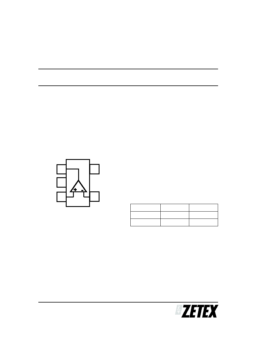
Video Amplifier
1
OUT
+IN
-IN
V+
V-
-
+
1
5
CONNECTION DIAGRAM
ADVANCED INFORMATION
ZXFV202
ABSOLUTE MAXIMUM RATINGS
Supply Voltage
±5.25V
Inputs to ground
Outputs to ground
Operating Temperature Range
-40∞C to 85∞C Storage -65∞C to 150∞C
Continuous Power Dissipation
250mW
Thermal resistance
250∞C/W
The power dissipation of the device including the loads must be designed to keep t
j
below 150∞
C
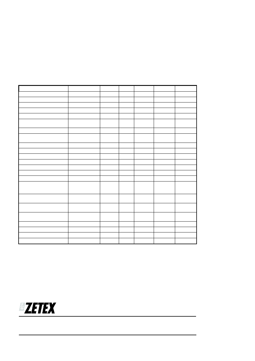
ELECTRICAL CHARACTERISTICS
Test Conditions: Vcc=±5V, Tamb= 25C unless otherwise stated. Rf = 1k
,
R
L
= 150
, C
L
<= 10pF
Parameter
Conditions
Test
Min.
Typical
Max.
Units
Supply Voltage V+
4.75
5
5.25
V
Supply Voltage V-
-5.25
-5
-4.75
V
Supply current
P
7
mA
Input Common mode
Voltage
P
±3
V
Input offset voltage
P
-10
±3
10
mV
Input bias current non
inverting input
P
+10
-4.5
µA
µA
Input Resistance
P
3
7
M
Output voltage swing
P
±3
V
Output drive current
P
40
mA
Positive PSRR
-55
dB
Negative PSRR
-57
dB
Bandwidth
Av= +1
C
300
MHz
Slew rate
Av= +1
Av = +2
Av = +10
400
400
V/µs
Rise time
Vout =
±
1 V,
10% - 90%
4.0
ns
Fall time
Vout = ±1V,
10% - 90%
3.2
ns
Propagation delay
Vout = +2 V,
50%
4
ns
Open loop gain
53
dB
Differential Gain
RL = 150
0.01
%
Differential phase
RL = 150
0.01
deg
Test: P=Production tested, C= Characterised
Zetex plc.
Fields New Road, Chadderton, Oldham, OL9-8NP, United Kingdom.
Telephone: (44)161 622 4422 (Sales), (44)161 622 4444 (General Enquiries)
Fax: (44)161 622 4420
Zetex GmbH
Zetex Inc.
Zetex (Asia) Ltd.
These are supported by
Streitfeldstraþe 19
47 Mall Drive, Unit 4
3701-04 Metroplaza, Tower 1
agents and distributors in
D-81673 M¸nchen
Commack NY 11725
Hing Fong Road,
major countries world-wide
Germany
USA
Kwai Fong, Hong Kong
© Zetex plc 2000
Telefon: (49) 89 45 49 49 0
Telephone: (631) 543-7100
Telephone:(852) 26100 611
Fax: (49) 89 45 49 49 49
Fax: (631) 864-7630
Fax: (852) 24250 494
Internet:http://www.zetex.com
This publication is issued to provide outline information only which (unless agreed by the Company in writing) may not be used, applied or reproduced for
any purpose or form part of any order or contract or be regarded as a representation relating to the products or services concerned. The Company reserves
the right to alter without notice the specification, design, price or conditions of supply of any product or service.