 | –≠–Ľ–Ķ–ļ—ā—Ä–ĺ–Ĺ–Ĺ—č–Ļ –ļ–ĺ–ľ–Ņ–ĺ–Ĺ–Ķ–Ĺ—ā: ZXFV203 | –°–ļ–į—á–į—ā—Ć:  PDF PDF  ZIP ZIP |

Issue 3 - October 2005
1
www.zetex.com
© Zetex Semiconductors plc 2005
ZXFV201, ZXFV202, ZXFV203, ZXFV204
Quad, single, triple and dual video amplifiers
Device description
The ZXFV201, ZXFV202, ZXFV203 and
ZXFV204 are quad, single, triple and dual,
respectively, high speed amplifiers designed
for video and other high speed applications.
Their low differential gain and phase
performance make them ideal for video
amplifier buffer applications.
The quad allows one IC to drive RGBS format
component video signals, while the triple
provides RGB component video buffer/driver.
The dual amplifier is a mainstay of the video
market providing two channels in the space of
1 single in SO8. The small size of the ZXFV202
in SOT23 allows it to be placed where needed
for position/size critical applications.
Together with high output drive and slew rate
capability, they bring high performance to
video applications.
Ordering information
Features
∑
High speed
∑
Gain of 1 - 3dB bandwidth 210MHz
∑
Slew rate 380V/Ķs
∑
Good video
∑
25 MHz 0.1dB bandwidth
∑
Differential gain 0.04%
∑
Differential phase 0.04į
∑
40mA output current @ 3V Output
∑
Characterized up to 300pF load
∑
Ī5 Volt supply operation
∑
Supply current 7.5mA per amplifier
Applications
∑
Industry standard pinouts
∑
Video gain stages
∑
CCTV buffer
∑
Video distribution
∑
RGB buffering
∑
Home theater
∑
High Speed ADC signal input drive
∑
Cable driving
Application diagram
Part number
Description
Reel
size
(inches)
Qty.
Part
mark
ZXFV202E5TA
Single
7
3,000
V202
ZXFV202E5TD
Single
7
500
V202
ZXFV202N8TA
Single
7
500
ZXFV202
ZXFV202N8TC
Single
13
2,500
ZXFV202
ZXFV204N8TA
Dual
7
500
ZXFV204
ZXFV204N8TC
Dual
13
2,500 ZXFV204
ZXFV203N14TA
Triple
7
500
ZXFV203
ZXFV203N14TC
Triple
13
2,500
ZXFV203
ZXFV201N14TA
Quad
7
500
ZXFV201
ZXFV201N14TC
Quad
13
2,500
ZXFV201
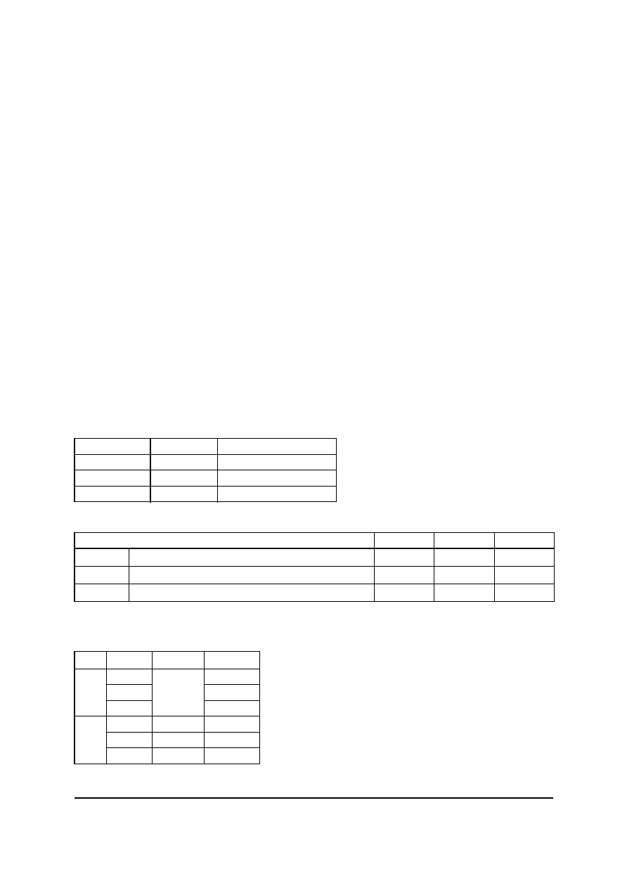
75 Co-ax
75 Co-ax
75
Back termination
+2
+2
Y
C
Dual amplifier S - video driver
ZXFV201, ZXFV202, ZXFV203, ZXFV204
Issue 3 - October 2005
2
www.zetex.com
© Zetex Semiconductors plc 2005
Power derating table
Recommended operating conditions
Recommended resistor values
V
SĪ
= 5V, C
L
= 10pF
Absolute maximum ratings over operating free-air temperature (unless
otherwise stated
(a)
)
NOTES:
(a) Stresses above those listed under Absolute maximum ratings may cause permanent damage to the device. This is a
stress rating only; functional operation of the device at these or any other conditions above those indicated in the
operational section of this specification is not implied. Exposure to absolute maximum rating conditions for extended
periods may affect device reliability.
Supply voltage (V
S+
to V
S-
)
-0.5V to +11V
Input voltage (V
IN-
, V
IN+
)
(b)
(b) During power-up and power-down, these voltage ratings require that signals be applied only when the power supply
is connected.
V
S-
-0.5V to V
S+
+0.5 V
Differential input voltage (V
ID
)
Ī3V
Inverting input current (I
IN-
)
(c)
(c) At high closed loop gains and low gain setting resistors care must be taken if large input signals are applied to the
device which cause the output stage to saturate for extended periods of time.
Ī5mA
Output current (continuous, T
J
< 110įC)
Ī60mA
Internal power dissipation
See power dissipation derating table
Storage temperature range
-65įC to +150įC
Operating ambient junction temperature (T
JMAX
) 150įC
Package
Theta-ja
Power rating at 25'C
SOT23-5
195įC/W
0.64W
SO8
168įC/W
0.74W
SO14
120įC/W
1.04W
Parameter
Min.
Max.
Unit
V
SĪ
Dual supply voltage range
Ī4.75
Ī5.25
V
V
CMR
Common mode input voltage range
-3
+3
V
T
A
Ambient temperature range
-40
85
įC
G
CL
R
F
R
G
Peaking
680
n/c
2 dB
1
820
0
1000
-2dB
430
430
2dB
2
470
470
1.5dB
560
560
0
ZXFV201, ZXFV202, ZXFV203, ZXFV204
Issue 3 - October 2005
3
www.zetex.com
© Zetex Semiconductors plc 2005
DC electrical characteristics (Ī5V power supplies, T
amb
= 25įC unless otherwise
stated. R
f
= 1k , R
L
= 150 , C
L
= 10pF)
Test - P = production tested. C = characterized
AC electrical characteristics (Ī5V, R
f
= 470 , G = 2, C
L
= 10pF, T
A
= 25įC, unless
otherwise stated)
Parameter
Conditions
Test
Min.
Typ. Max.
Unit
Supply voltage V+ operating range
4.75
5
5.25
V
Supply voltage V- operating range
-5.25
-5
-4.75
V
Supply current/per channel
P
5.0
7.5
10
mA
Input common mode voltage range
P
3
V
Input offset voltage
P
1
10
mV
Output offset voltage
P
2
20
mV
Input bias current, non-inverting input
P
5
10
A
Input resistance
P
1.5
2
6.5
M
Output voltage swing
I
OUT
= 40mA
P
3
V
Output drive current
V
IN
= 3V
P
40
mA
Positive PSRR
V+ = Ī0.25
P
49
57
dB
Negative PSRR
V- = Ī0.25
P
49
57
dB
Parameter Conditions
Min
Typ
Max
Unit
BW
-3
Bandwidth, -3dB
V
OUT
= 0.2V
PP
G = +2, R
F
= 470
210
MHz
V
OUT
= 0.2V
PP
G = +1, R
F
= 820
210
BW
0.1
Bandwidth, Ī0.1dB
V
OUT
= 0.2V
PP
30
MHz
SR
Slew Rate
V
OUT
= 2V
PP
G = +2, R
F
= 470
600
V/ s
V
OUT
= 2V
PP
G = +1, R
F
= 820
380
t
r
Rise time
V
OUT
= Ī1V, 10% - 90%
5.8
t
f
Fall time
4.6
ns
t
p
Propagation delay
V
OUT
= Ī2V, 10% - 90%
2.6
dG
Differential phase, NTSC NTSC/PAL, 280mV
PP
,
DC = -1.428V to +1.428 V
0.04
%
dP
Differential phase, NTSC
0.04į
ZXFV201, ZXFV202, ZXFV203, ZXFV204
Issue 3 - October 2005
4
www.zetex.com
© Zetex Semiconductors plc 2005
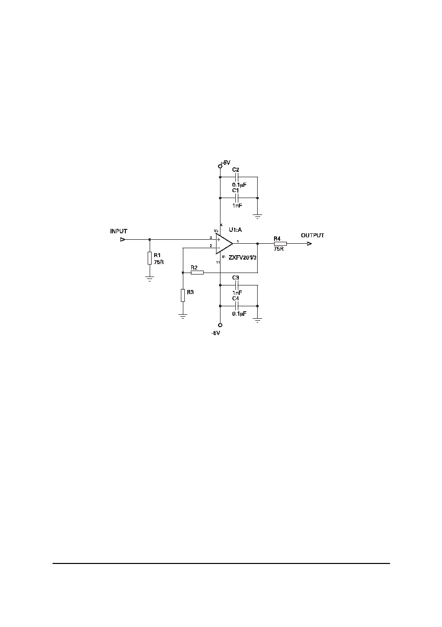
Applications information
A typical circuit application is shown in Figure 1. This is suitable for 75 transmission line
connections at both the input and the output and is useful for distribution of wide-band signals
such as video via cables. The 75 reverse terminating resistor R4 gives the correct matching
condition to a terminated video cable. The amplifier load is then 150 in parallel with the local
feedback network.
Figure 1
Typical video signal application circuit, gain = 2 (overall gain = 1 for 75 load
The wide bandwidth of this device necessitates some care in the layout of the printed circuit. A
continuous ground plane is required under the device and its signal connection paths, to provide
the shortest possible ground return paths for signals and power supply filtering. A double-sided
or multi-layer PCB construction is required, with plated-through via holes providing closely
spaced low-inductance connections from some components to the continuous ground plane.
For the power supply filtering, low inductance surface mount capacitors are normally required. It
has been found that very good RF decoupling is provided on each supply using a 1000pF NPO
size 0805 or smaller ceramic surface mount capacitor, closest to the device pin, with an adjacent
0.1 F X7R capacitor. Other configurations are possible and it may be found that a single 0.01 F
X7R capacitor on each supply gives good results. However this should be supported by larger
decoupling capacitors elsewhere on the printed circuit board. Values of 1 to 10 F are
recommended, particularly where the voltage regulators are located more than a few inches from
the device. These larger capacitors are recommended to be solid tantalum electrolytic or ceramic
types.
Note particularly that the inverting input of this current feedback type of amplifier is sensitive to
small amounts of capacitance to ground which occur as part of the practical circuit board layout.
This capacitance affects bandwidth, frequency response peaking and pulse overshoot. Therefore
to minimize this capacitance, the feedback components R2 and R3 of Figure 1 should be
positioned as close as possible to the inverting input connection.
470
470

ZXFV201, ZXFV202, ZXFV203, ZXFV204
Issue 3 - October 2005
5
www.zetex.com
© Zetex Semiconductors plc 2005
The frequency response and pulse response will vary according to particular values of resistors
and layout capacitance. The response can be tailored for the application to some extent by choice
of the value of feedback resistor. Figures 2 and 3 show the small signal unity gain and gain of 2
frequency responses.
Figure 2
Unity gain small signal bandwidth
Figure 3
Gain of 2 small signal bandwidth
-6
-3
0
3
1
10
100
1000
Frequency (MHz)
Gai
n
(dB
)
R
F
= 680
R
F
= 820
R
F
= 1k
V
IN
= 200mV
PP
V
SĪ
=
Ī
5V
R
L
=
150
T
A
= 25
į
G
=
1
C
L
=
10pF
0
3
6
9
1
10
100
1000
Frequency (MHz)
Gain (dB)
R
F
= 430
R
F
= 470
R
F
= 560
V
IN
= 200mV
PP
V
SĪ
=
Ī
5V
R
L
=
150
T
A
= 25
į
G
=
2
C
L
=
10pF