1
S E M I C O N D U C T O R S
DESCRIPTION
The ZXLD1100 is a PFM inductive boost converter
designed for driving 2, 3 or 4 series connected white
LEDs from a Li-Ion cell and up to 8 LEDs from a 5V
supply. The device operates from an input supply of
between 2.5V and 5.5V and provides an adjustable
output current of up to 50mA.
The ZXLD1100 includes the output switch and peak
current sense resistor, and can operate with a
maximum output voltage of 28V.
Quiescent current is typically 60 A and a shutdown
function is provided to reduce this current to less than
500nA in the 'off' state.
ADVANCED FEATURES
∑
Internal 30V NDMOS switch, current sense and
open circuit protection
∑
True Analog Dimming via PWM
FEATURES
∑
Low profile SC70 6 pin package
∑
Internal PWM filter for flicker free output
∑
High efficiency (80% typ)
∑
Wide input voltage range: 2.5V to 5.5V
∑
Up to 50mA output current
∑
Low quiescent current: (60 A typ)
∑
500nA maximum shutdown current
∑
Up to 1MHz switching frequency
∑
Low external component count
∑
Inherently matched LED currents
Output current can be adjusted by applying a PWM
control signal to the 'Enable' pin. Depending upon the
control frequency, this will provide either a continuous
or a 'chopped' output current. The PWM filter
components are contained within the chip.
The ZXLD1100 contains an internal avalanche diode to
protect the output switch. This allows the device to
operate indefinitely if the load is open circuit. Input
supply current during this condition is less than 1mA.
The device is assembled in a low profile SC70-6 pin
package with industry standard pinout.
APPLICATIONS
∑
Mobile phones
∑
Digital cameras
∑
PDAs
∑
LCD modules
∑
Portable internet appliances
∑
Palmtop computers
ZXLD1100
ISSUE 4 - JULY 2004
ADJUSTABLE LED DRIVER WITH INTERNAL SWITCH AND OPEN
CIRCUIT PROTECTION IN SC70-6
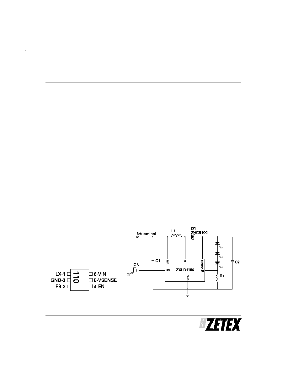
PIN CONNECTIONS
TYPICAL APPLICATION CIRCUIT
ZXLD1100
S E M I C O N D U C T O R S
ISSUE 4 - JULY 2004
2
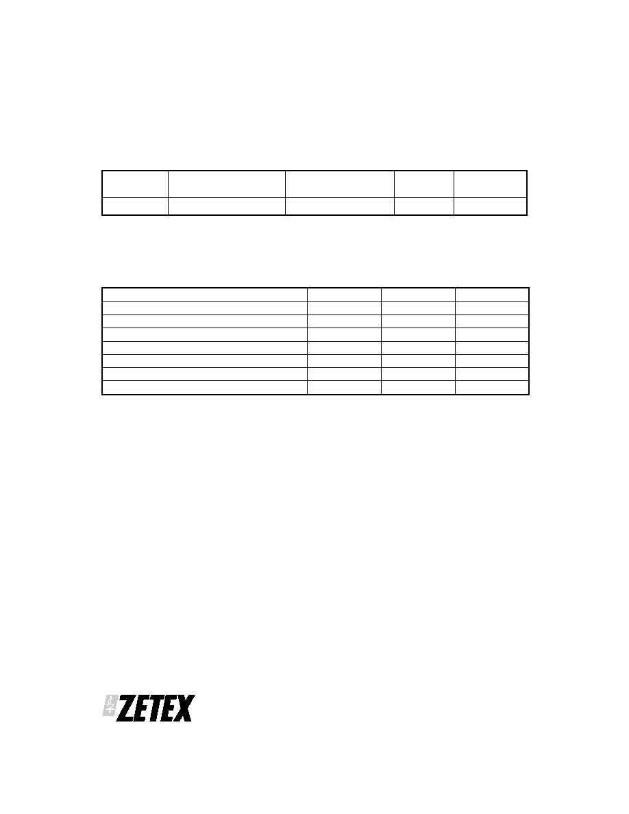
PARAMETER
SYMBOL
LIMIT
UNIT
Input voltage
(V
IN
)
7
V
LX output voltage
(V
LX
)
30
V
Switch output current
(I
LX
)
500
mA
Power dissipation
(PD)
300
mW
Operating temperature
(T
OP
)
-40 to 85
∞C
Storage temperature
(T
ST
)
-55 to 150
∞C
Junction temperature
(T
j MAX
)
125
∞C
ABSOLUTE MAXIMUM RATINGS (Voltages to GND unless otherwise stated)
DEVICE
DEVICE DESCRIPTION
TEMPERATURE RANGE
PART MARK
TAPING
OPTIONS
ZXLD1100H6
Boost convertor in SC70-6
-40 to +85∞C
110
TA, TC
ORDERING INFORMATION
ZXLD1100H6TA = 7" reel of 3,000 devices
ZXLD1100H6TC = 13" reel of 10,000 devices
ZXLD1100
S E M I C O N D U C T O R S
ISSUE 4 - JULY 2004
3
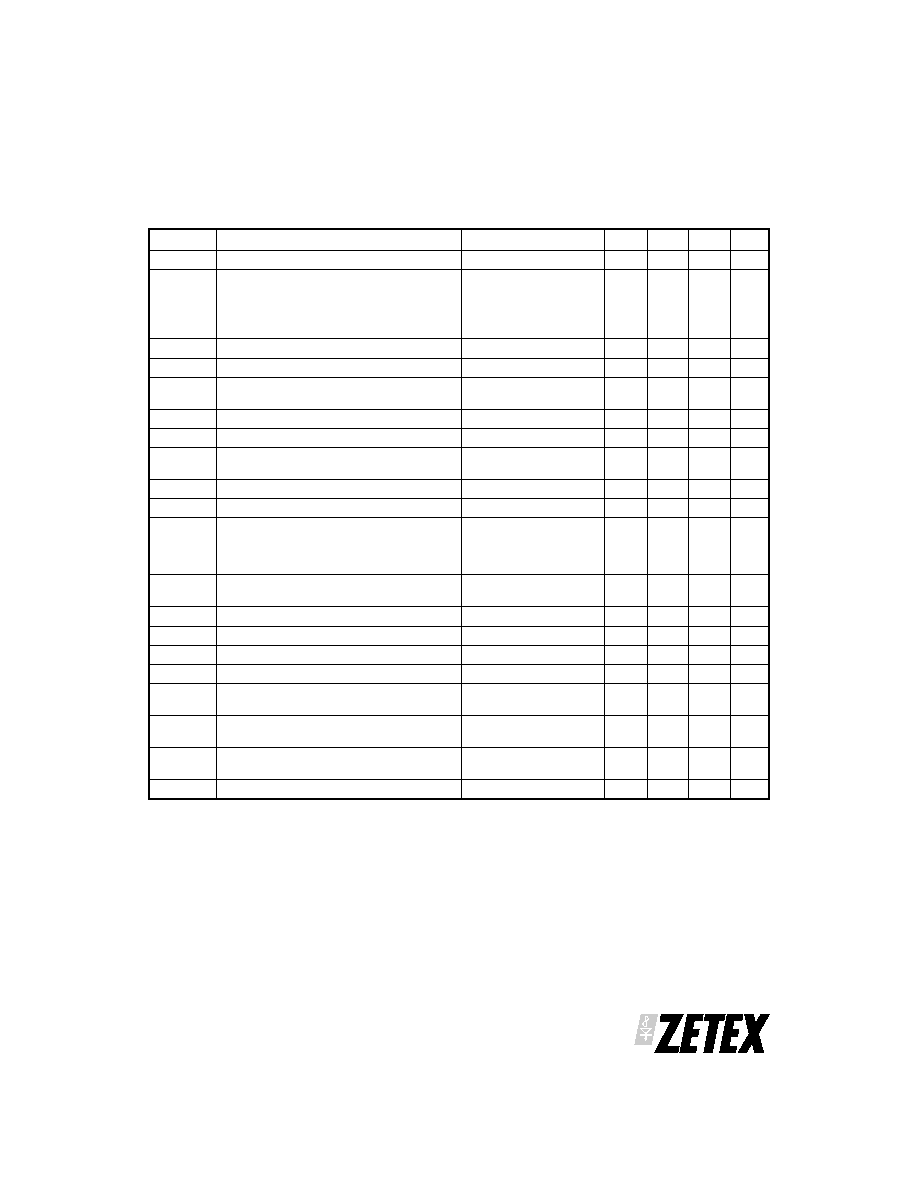
SYMBOL
PARAMETER
CONDITIONS
MIN.
TYP.
MAX.
UNIT
V
IN
Input voltage
2.5
5.5
V
I
IN
Supply current
Quiescent
Shutdown
V
EN
= V
IN
, I
LX
= 0,
Output not switching
V
EN
= 0V
60
100
500
A
nA
V
FB
FB pin control voltage
90.5
109.5
mV
I
FB
FB pin input current
100
nA
f
LX
Operating frequency
L=10 H, V
OUT
=10V,
I
OUT
=20mA
0.35
1
MHz
T
OFF
LX output 'OFF' time
350
500
ns
T
ON
LX output 'ON' time
(2)
5
µs
I
LXpk
Switch peak current limit
L=10 H, V
OUT
=10V,
I
OUT
=20mA
320
mA
R
LX
Switch 'On' resistance
1.5
I
LX(leak)
Switch leakage current
V
LX
=20V
1
µA
V
OUT
Controller output voltage
Normal operation
VSENSE pin
open-circuit or
grounded
28
V
V
OUT(MAX)
Controller output voltage with output
open circuit
(3)
VSENSE connected to
Vout
25
30
V
V
ENH
EN pin High level Input voltage
Device active
1.5
V
IN
V
V
ENL
EN pin Low level Input voltage
Device in shutdown
0.4
V
I
ENL
EN pin Low level input current
V
EN
=0V
-100
nA
I
ENH
EN pin High level input current
V
EN
=V
IN
1
A
T
EN(hold)
EN pin turn off delay
(4)
V
EN
switched from
high to low
120
µs
T/T
PWM duty cycle range at `EN' input for
filtered PWM control
(5)
10kHz < f < 100kHz,
V
ENH
=V
IN
20
100
%
f
LPF
Internal PWM low pass filter cut-off
frequency
4
kHz
A
LPF
Filter attenuation
f=30kHz
52.5
dB
ELECTRICAL CHARACTERISTICS (at V
IN
= 3V, T
amb
= 25∞C unless otherwise stated
(1)
)
NOTES:
(1) Production testing of the device is performed at 25∞C. Functional operation of the device over a -40∞C to +85∞C temperature range is
guaranteed by design, characterization and process control.
(2) Nominal 'on' time (T
ONnom
) is defined by the input voltage (V
IN
), coil inductance (L) and peak current (I
LXpkdc
) according to the expression:
T
ONnom
= {I
LX(pkdc
) x L/V
IN
} +200ns.
(3) When using the open circuit protection feature, the maximum output voltage under normal operation should be maintained below the
minimum value specified, in order to prevent possible disturbance of the current control loop.
(4) This is the time for which the device remains active after the EN pin has been asserted low. This delay is necessary to allow the output to be
maintained during dc PWM mode operation.
(5) The minimum PWM signal frequency during this mode of operation is to ensure that the device remains active during PWM control. This
provides a continuous dc output current. For lower frequencies, the device will be gated 'on' and 'off' during PWM control.
(6) The maximum PWM signal frequency during this mode of operation should be kept as low as possible to minimize errors due to the turn-off
delay of the device (see Enable pin turn-off delay).

ZXLD1100
S E M I C O N D U C T O R S
ISSUE 4 - JULY 2004
4
BLOCK DIAGRAM
PIN NO.
NAME
DESCRIPTION
1
LX
Output of NDMOS switch
2
GND
Ground (0V)
3
FB
Feedback pin for current control loop (connect resistor R1
from this pin to GND for output current I=100mV/ R1)
4
EN
Enable input (active high to turn on device)
Also used to adjust output current by PWM signal.
Connect to V
in
for permanent operation.
5
VSENSE
Output voltage sense (used for open circuit protection).
Connect to GND if not required.
6
V
IN
Input voltage (2.5V to 5.5V). Decouple with capacitor close
to device.
PIN DESCRIPTION

DEVICE DESCRIPTION
The device is a PFM flyback dc-dc boost converter,
working in discontinuous mode.
With reference to the chip block diagram and typical
application circuit, the operation of the device is as
follows:
Control loop
When 'EN' is high, the control circuits become active
and the low side of the coil (L1) is switched to ground
via NDMOS transistor (MN). The current in L1 is
allowed to build up to an internally defined level
(nominally 320mA) before MN is turned off. The energy
stored in L1 is then transferred to the output capacitor
(C2) via schottky diode (D1). When the voltage on C2
has risen above the threshold voltage of the series
connected LEDs, current will flow through external
sense resistor R1. The voltage developed across R1 is
sensed at pin 'FB' and compared to a 100mV reference
voltage (V
REF
). A comparator senses when the
feedback voltage is above V
REF
and its output is used to
control the 'off' time of the output switch. The control
loop is self-oscillating, producing pulses of up to 5 s
maximum duration (switch 'on'), at a frequency that
varies in proportion to the LED current. The feedback
loop maintains a voltage of V
REF
at the FB pin and
therefore defines a maximum LED current equal to V
REF
divided by R1. The minimum 'off' time of the output
switch is fixed at 0.5 s nominal, to allow time for the
coil's energy to be dissipated before the switch is
turned on again. This maintains stable and efficient
operation in discontinuous mode.
Open circuit protection
There is an internal avalanche diode between the
V
SENSE
and FB pins of the device. This diode, together
with the associated resistors provides open circuit
protection when the V
SENSE
pin is connected to the
output voltage. In the event of an open circuit
condition, the output voltage will rise above the
breakdown voltage of the internal diode, which will
then conduct and override the control signal from the
current sense resistor. This maintains the output
voltage at a level below the breakdown voltage of the
output switch. Supply current in this condition will fall
to a low value as the control loop provides only the bias
current for the diode.
Filtered PWM operation
The input of an internal low pass filter is switched to
V
REF
when the EN pin is high and switched to ground
when the EN pin is low. The output of this filter drives
the comparator within the control loop. A continuous
high state on EN therefore provides a filtered voltage of
value V
REF
to the comparator. However, by varying the
duty cycle of the EN signal at a suitably high frequency
(f>10kHz), the control loop will see a voltage, that has
an average value equal to the duty cycle multiplied by
V
REF
. This provides a means of adjusting the output
current to a lower value. It also allows the device to be
both turned on and adjusted with a single signal at the
'EN' pin. The output during this mode of operation will
be a dc current equal to (V
REF
/R1) x duty cycle
Gated PWM operation
The internal circuitry of the ZXLD1100 is turned off
when no signal is present on the 'EN' pin for more than
120 s (nominal). A low frequency signal applied to the
EN pin will therefore gate the device 'on' and 'off' at the
gating frequency and the duty cycle of this signal can
be varied to provide a 'chopped' output current equal
to (V
REF
/R1) x duty cycle. For best accuracy, the gating
frequency should be made as low as possible (e.g.
below 1kHz), such that the turn off delay of the chip is
only a small proportion of the gating period
Further details of setting output current are given in the
applications section under brightness control.
ZXLD1100
S E M I C O N D U C T O R S
ISSUE 4 - JULY 2004
5