S E M I C O N D U C T O R S
SUMMARY
V
(BR)DSS
= 60V : R
DS(on)
= 0.3 ; I
D
= 1.6A
DESCRIPTION
This new generation of trench MOSFETs from Zetex
utilizes a unique structure that combines the benefits of
low on-resistance with fast switching speed. This
makes them ideal for high efficiency, low voltage,
power management applications.
FEATURES
∑
Compact package
∑
Low on state losses
∑
Low drive requirements
∑
Operates up to 60V
∑
1 Amp continuous rating
APPLICATIONS
∑
Motor control
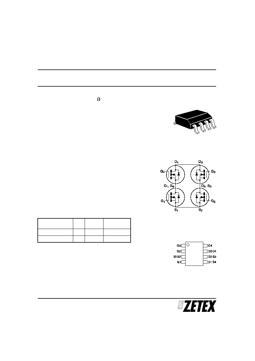
DEVICE MARKING
∑
ZXMH
N6A07
ZXMHN6A07T8
ISSUE 2 - MAY 2004
60V N-CHANNEL MOSFET H-BRIDGE
1
SM8
TOP VIEW
PINOUT
DEVICE
REEL
SIZE
TAPE
WIDTH
QUANTITY PER
REEL
ZXMHN6 A0 7 T8 TA
7"
12mm
1,000 units
ZXMHN6 A0 7 T8 TC
13"
12mm
4,000 units
ORDERING INFORMATION
ZXMHN6A07T8
S E M I C O N D U C T O R S
ISSUE 2 - MAY 2004
2
PARAMETER
SYMBOL
LIMIT
UNIT
Drain-source voltage
V
DSS
60
V
Gate-source voltage
V
GS
± 20
V
Continuous drain current (V
GS
= 1 0 V; T
A
= 2 5 ∞ C)
(b) (d)
(V
GS
= 1 0 V; T
A
= 7 0 ∞ C)
(b) (d)
(V
GS
= 1 0 V; T
A
= 2 5 ∞ C)
(a) (d)
I
D
1.6
1.3
1.4
A
A
A
Pulsed drain current
(c )
I
DM
9
A
Continuous source current (body diode)
(b) (d)
I
S
1
A
Pulsed source current (body diode)
(c )
I
SM
9
A
Total power dissipation at T
A
= 2 5 ∞ C
Any Single transistor " on"
(a) (d)
Single transistor ` on'
(b) (d)
Two transistors ` on' equally
(a) (e)
P
TOT
1.1
1.4
1.6
W
W
W
Linear derating factor above 2 5 ∞ C
(a)
Single transistor " on"
(a) (d)
Single transistor ` on'
(b) (d)
Two transistors ` on' equally
(a) (e)
8.8
11.2
13.2
mW/∞ C
mW/∞ C
mW/∞ C
Thermal resistance - junction to ambient
Single transistor " on"
(a) (d)
Single transistor " on"
(b) (d)
Two transistors ` on' equally
(a) (e)
R
t h(j-amb)
114
89
76
∞ C/W
∞ C/W
∞ C/W
Operating and storage temperature range
T
j
, T
st g
-55 to + 150
∞ C
ABSOLUTE MAXIMUM RATINGS
(a) For a device mounted on 50mm x 50mm x 1.6mm FR4 PCB with a high coverage of single sided 2oz weight copper in still air conditions with the
heat sink split into three equal areas, one for each drain connection.
(b) For a device surface mounted on a FR4 PCB at t
= 10 sec.
(c) Repetitive rating on 50mm x 50mm x 1.6mm FR4 PCB, duty cycle 2% , pulse width 300 S in still air conditions with the heat sink split into three
equal areas, one for each drain connection.
(d) For device with one active die.
(e) For any two die not sharing the same drain connection.
ZXMHN6A07T8
S E M I C O N D U C T O R S
ISSUE 2 - MAY 2004
4
PARAMETER
SYMBOL
MIN.
TYP.
MAX.
UNIT CONDITIONS
STATIC
Drain-source breakdown voltage
V
(BR)DSS
60
V
I
D
= 2 5 0 A, V
GS
= 0 V
Zero gate voltage drain current
I
DSS
1.0
A
V
DS
= 6 0 V , V
GS
= 0 V
Gate-body leakage
I
GSS
100
nA
V
GS
= ± 2 0 V , V
DS
= 0 V
Gate-source threshold voltage
V
GS(t h)
1.0
3.0
V
I
D
= 2 5 0 A, V
DS
= V
GS
Static drain-source on-state
resistance
(1 )
R
DS(on)
0.3
0.45
V
GS
= 1 0 V , I
D
= 1 . 8 A
V
GS
= 4 . 5 V , I
D
= 1 . 3 A
Forward transconductance
(1 ) (3 )
g
f s
2.3
S
V
DS
= 1 5 V , I
D
= 1 . 8 A
DYNAMIC
(3 )
Input capacitance
C
iss
166
pF
V
DS
= 4 0 V , V
GS
= 0 V
f= 1 MHz
Output capacitance
C
oss
20
pF
Reverse transfer capacitance
C
rss
9
pF
SWITCHING
(2 ) (3 )
Turn-on-delay time
t
d(on)
1.8
ns
V
DD
= 3 0 V , I
D
= 1 . 8 A
R
G
@ 6.0W, V
GS
= 1 0 V
Rise time
t
r
1.4
ns
Turn-off delay time
t
d(of f )
4.9
ns
Fall time
t
f
2.0
ns
Total gate charge
Q
g
3.2
nC
V
DS
= 3 0 V , V
GS
= 1 0 V
I
D
= 1 . 8 A
Gate-source charge
Q
gs
0.7
nC
Gate drain charge
Q
gd
0.8
nC
SOURCE-DRAIN DIODE
Diode forward voltage
(1 )
V
SD
0.95
V
T
j
= 2 5 ∞ C, I
S
= 0 . 4 5 A,
V
GS
= 0 V
Reverse recovery time
(3 )
t
rr
21
ns
T
j
= 2 5 ∞ C, I
F
= 1 . 0 A,
di/ dt= 1 0 0 A/ s
Reverse recovery charge
(3 )
Q
rr
21
nC
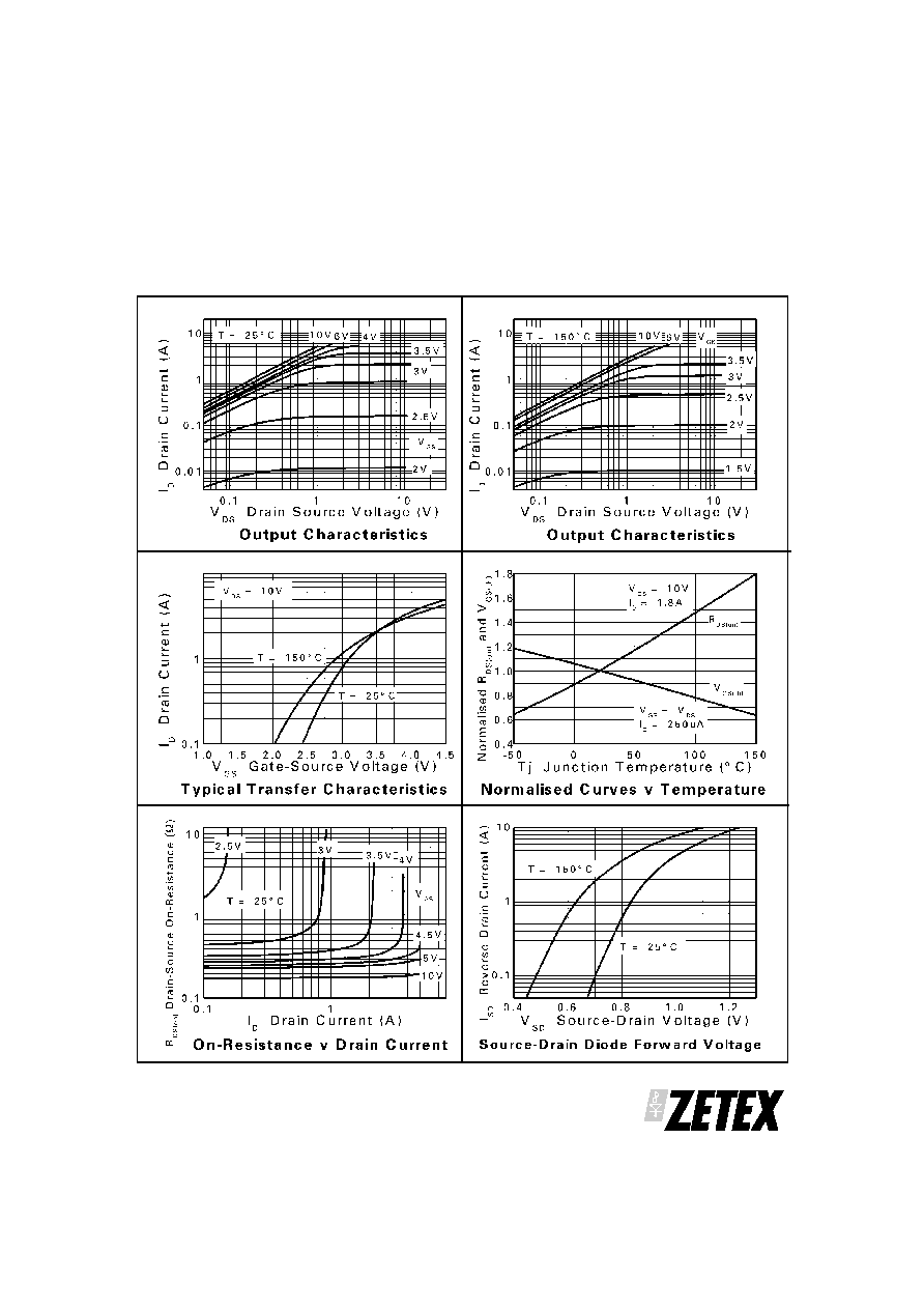
ELECTRICAL CHARACTERISTICS (at T
amb
= 25∞ C unless otherwise stated)
NOTES
(1) Measured under pulsed conditions. Pulse width
300 s; duty cycle
2% .
(2) Switching characteristics are independent of operating junction temperature.
(3) For design aid only, not subject to production testing.