SUMMARY
V
(BR)DSS
= 20V; R
DS(ON)
= 0.12 ; I
D
= 3A
DESCRIPTION
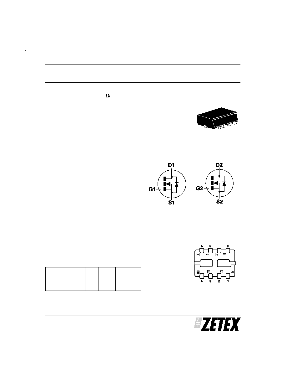
Packaged in the new innovative 3mm x 2mm MLP(Micro Leaded Package)
outline this dual 20V N channel Trench MOSFET utilizes a unique structure
combining the benefits of Low on-resistance with fast switching speed. This
makes them ideal for high efficiency, low voltage power management
applications. Users will also gain several other key benefits:
Performance capability equivalent to much larger packages
Improved circuit efficiency & power levels
PCB area and device placement savings
Reduced component count
FEATURES
∑
Low On - Resistance
∑
Fast switching speed
∑
Low threshold
∑
Low gate drive
∑
3mm x 2mm MLP
APPLICATIONS
∑
DC-DC Converters
∑
Power Management Functions
∑
Disconnection switches
∑
Motor Control
DEVICE MARKING
DNA
ZXMN2AM832
ISSUE 3 - JANUARY 2005
S E M I C O N D U C T O R S
1
MPPSTM Miniature Package Power Solutions
DUAL 20V N-CHANNEL ENHANCEMENT MODE MOSFET
DEVICE
REEL
TAPE
WIDTH
QUANTITY
PER REEL
ZXMN2AM832TA
7'`
8mm
3000 units
ZXMN2AM832TC
13'`
8mm
10000 units
ORDERING INFORMATION
3x2mm Dual Die MLP
7
3mm x 2mm Dual MLP
underside view
PINOUT

ZXMN2AM832
ISSUE 3 - JANUARY 2005
2
S E M I C O N D U C T O R S
PARAMETER
SYMBOL
VALUE
UNIT
Junction to Ambient (a)(f)
R
JA
83.3
∞C/W
Junction to Ambient (b)(f)
R
JA
51
∞C/W
Junction to Ambient (c)(f)
R
JA
125
∞C/W
Junction to Ambient (d)(f)
R
JA
111
∞C/W
Junction to Ambient (d)(g)
R
JA
73.5
∞C/W
Junction to Ambient (e)(g)
R
JA
41.7
∞C/W
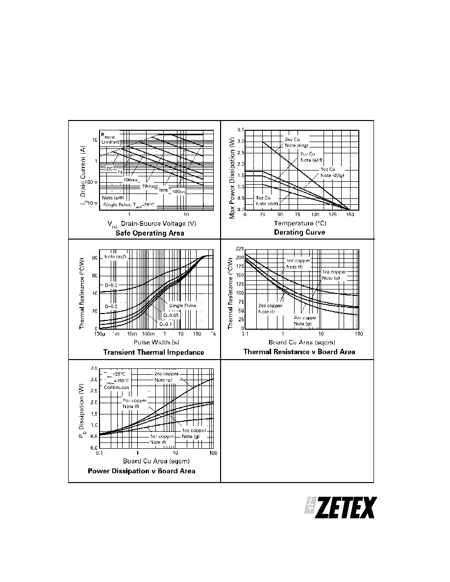
THERMAL RESISTANCE
Notes
(a) For a dual device surface mounted on 8 sq cm single sided 2oz copper on FR4 PCB, in still air conditions with all exposed pads attached. The
copper area is split down the centre line into two separate areas with one half connected to each half of the dual device.
(b) Measured at t<5 secs for a dual device surface mounted on 8 sq cm single sided 2oz copper on FR4 PCB, in still air conditions with all exposed
pads attached. The copper area is split down the centre line into two separate areas with one half connected to each half of the dual device.
(c) For a dual device surface mounted on 8 sq cm single sided 2oz copper on FR4 PCB, in still air conditions with minimal lead connections only.
(d) For a dual device surface mounted on 10 sq cm single sided 1oz copper on FR4 PCB, in still air conditions with all exposed pads attached
attached. The copper area is split down the centre line into two separate areas with one half connected to each half of the dual device.
(e) For a dual device surface mounted on 85 sq cm single sided 2oz copper on FR4 PCB, in still air conditions with all exposed pads attached
attached. The copper area is split down the centre line into two separate areas with one half connected to each half of the dual device.
(f) For a dual device with one active die.
(g) For dual device with 2 active die running at equal power.
(h) Repetitive rating - pulse width limited by max junction temperature. Refer to Transient Thermal Impedance graph.
(i) The minimum copper dimensions required for mounting are no smaller than the exposed metal pads on the base of the device as shown in the
package dimensions data. The thermal resistance for a dual device mounted on 1.5mm thick FR4 board using minimum copper 1 oz weight, 1mm
wide tracks and one half of the device active is Rth = 250∞C/W giving a power rating of Ptot = 500mW.
PARAMETER
SYMBOL
N-Channel
UNIT
Drain-Source Voltage
V
DSS
20
V
Gate-Source Voltage
V
GS
12
V
Continuous Drain Current @V
GS
=10V; T
A
=25 C
(b) (f)
@V
GS
=10V; T
A
=70 C
(b) (f)
@V
GS
=10V; T
A
=25 C
(a) (f)
I
D
3.7
3.0
2.9
A
A
A
Pulsed Drain Current
I
DM
13
A
Continuous Source Current (Body Diode)
(b) (f)
I
S
3.0
A
Pulsed Source Current (Body Diode)
I
SM
13
A
Power Dissipation at TA=25∞C
(a) (f)
Linear Derating Factor
P
D
1.5
12
W
mW/∞C
Power Dissipation at TA=25∞C
(b) (f)
Linear Derating Factor
P
D
2.45
19.6
W
mW/∞C
Power Dissipation at TA=25∞C
(c) (f)
Linear Derating Factor
P
D
1
8
W
mW/∞C
Power Dissipation at TA=25∞C (
d) (f)
Linear Derating Factor
P
D
1.13
9
W
mW/∞C
Power Dissipation at TA=25∞C
(d) (g)
Linear Derating Factor
P
D
1.7
13.6
W
mW/∞C
Power Dissipation at TA=25∞C
(e) (g)
Linear Derating Factor
P
D
3
24
W
mW/∞C
Operating and Storage Temperature Range
T
j
:T
stg
-55 to +150
∞C
ABSOLUTE MAXIMUM RATINGS.
ZXMN2AM832
ISSUE 3 - JANUARY 2005
4
S E M I C O N D U C T O R S
PARAMETER
SYMBOL
MIN.
TYP.
MAX.
UNIT CONDITIONS.
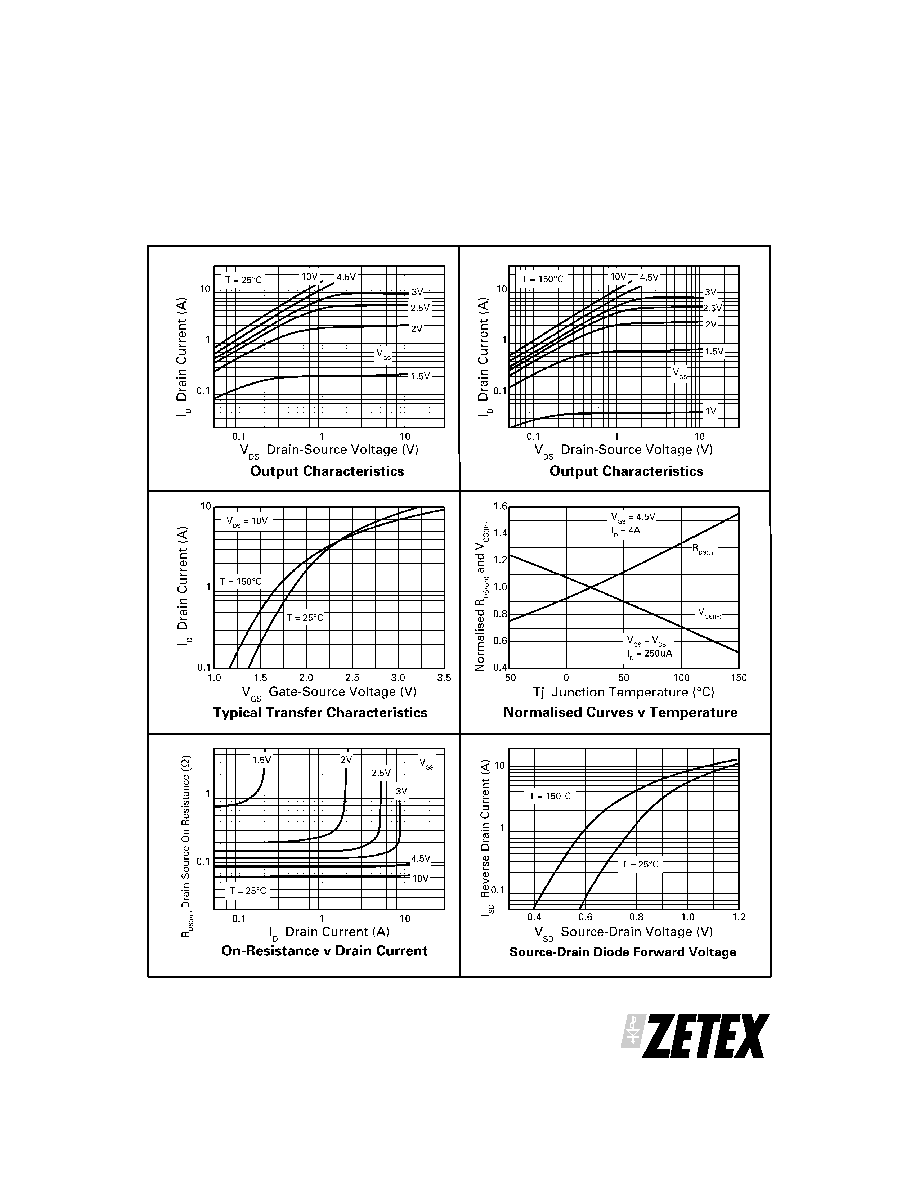
STATIC
Drain-Source Breakdown Voltage
V
(BR)DSS
20
V
I
D
=250 A, V
GS
=0V
Zero Gate Voltage Drain Current
I
DSS
1
A
V
DS
=20V, V
GS
=0V
Gate-Body Leakage
I
GSS
100
nA
V
GS
=
±12V, V
DS
=0V
Gate-Source Threshold Voltage
V
GS(th)
0.7
V
I
D
=250 A, V
DS
=V
GS
Static Drain-Source On-State
Resistance
(1)
R
DS(on)
0.09
0.12
0.30
V
GS
=4.5V, I
D
=4A
V
GS
=2.5V, I
D
=1.5A
Forward Transconductance
(3)
g
fs
6.2
S
V
DS
=10V,I
D
=4A
DYNAMIC
(3)
Input Capacitance
C
iss
299
pF
V
DS
=15 V, V
GS
=0V,
f=1MHz
Output Capacitance
C
oss
60
pF
Reverse Transfer Capacitance
C
rss
33
pF
SWITCHING
(2) (3)
Turn-On Delay Time
t
d(on)
2.31
ns
V
DD
=10V, I
D
=4A
R
G
6.0 , V
GS
=5V
Rise Time
t
r
2.60
ns
Turn-Off Delay Time
t
d(off)
1.55
ns
Fall Time
t
f
1.31
ns
Total Gate Charge
Q
g
3.1
nC
V
DS
=10V,V
GS
=4.5V,
I
D
=4A
Gate-Source Charge
Q
gs
0.7
nC
Gate-Drain Charge
Q
gd
1.0
nC
SOURCE-DRAIN DIODE
Diode Forward Voltage
(1)
V
SD
0.9
0.95
V
T
J
=25∞C, I
S
=3.2A,
V
GS
=0V
Reverse Recovery Time
(3)
t
rr
23
ns
T
J
=25∞C, I
F
=4A,
di/dt= 100A/ s
Reverse Recovery Charge
(3)
Q
rr
5.65
nC
ELECTRICAL CHARACTERISTICS (at T
amb
= 25∞C unless otherwise stated).
NOTES
(1) Measured under pulsed conditions. Width
300 s. Duty cycle
2%.
(2) Switching characteristics are independent of operating junction temperature.
(3) For design aid only, not subject to production testing.