SUMMARY
V
(BR)DSS
= 60V; R
DS(ON)
= 0.14
I
D
= 3.8A
DESCRIPTION
This new generation of TRENCH MOSFETs from Zetex utilises a unique structure
that combines the benefits of low on-resistance with fast switching speed. This
makes them ideal for high efficiency, low voltage, power management applications.
FEATURES
∑
Low on-resistance
∑
Fast switching speed
∑
Low threshold
∑
Low gate drive
∑
SOT223 package
APPLICATIONS
∑
DC - DC Converters
∑
Power Management Functions
∑
Relay and Solenoid driving
∑
Motor control
DEVICE MARKING
∑
ZXMN
6A11
ZXMN6A11G
ISSUE 1 - MARCH 2002
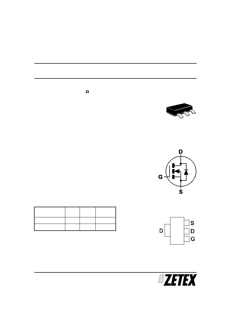
60V N-CHANNEL ENHANCEMENT MODE MOSFET
1
Top View
SOT223
DEVICE
REEL
SIZE
TAPE
WIDTH
QUANTITY
PER REEL
ZXMN6A11GFTA
7"
12mm
1000 units
ZXMN6A11GFTC
13"
12mm
4000 units
ORDERING INFORMATION
ZXMN6A11G
ISSUE 1 - MARCH 2002
2
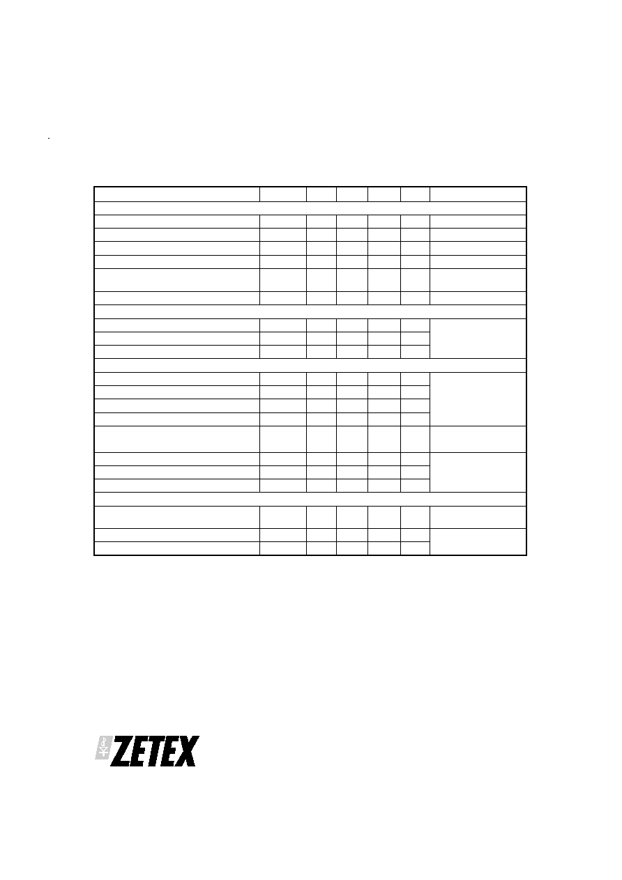
PARAMETER
SYMBOL
LIMIT
UNIT
Drain-Source Voltage
VDSS
60
V
Gate-Source Voltage
VGS
20
V
Continuous Drain Current VGS=10V; TA=25∞C(b)
VGS=10V; TA=70∞C(b)
VGS=10V; TA=25∞C(a)
ID
3.8
3.0
2.7
A
Pulsed Drain Current (c)
IDM
10
A
Continuous Source Current (Body Diode) (b)
IS
5
A
Pulsed Source Current (Body Diode)(c)
ISM
10
A
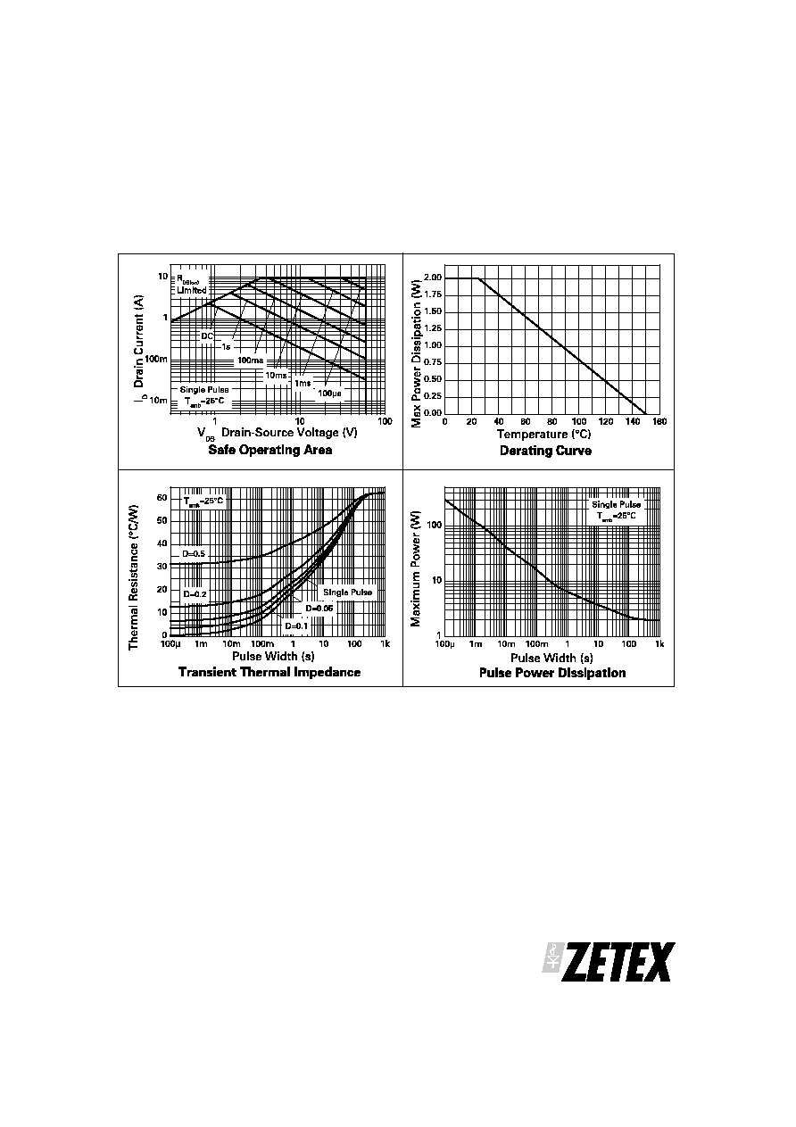
Power Dissipation at TA=25∞C (a)
Linear Derating Factor
PD
2.0
16
W
mW/∞C
Power Dissipation at TA=25∞C (b)
Linear Derating Factor
PD
3.9
31
W
mW/∞C
Operating and Storage Temperature Range
Tj:Tstg
-55 to +150
∞C
ABSOLUTE MAXIMUM RATINGS
PARAMETER
SYMBOL
VALUE
UNIT
Junction to Ambient (a)
R
JA
62.5
∞C/W
Junction to Ambient (b)
R
JA
32
∞C/W
THERMAL RESISTANCE
NOTES
(a) For a device surface mounted on 25mm x 25mm FR4 PCB with high coverage of single sided 1oz copper, in still air conditions
(b) For a device surface mounted on FR4 PCB measured at t 5 secs.
(c) Repetitive rating 25mm x 25mm FRA PCB, D=0.05 pulse width = 10 s - pulse width limited by maximum junction temperature.
ZXMN6A11G
ISSUE 1 - MARCH 2002
4
PARAMETER
SYMBOL
MIN.
TYP.
MAX.
UNIT
CONDITIONS.
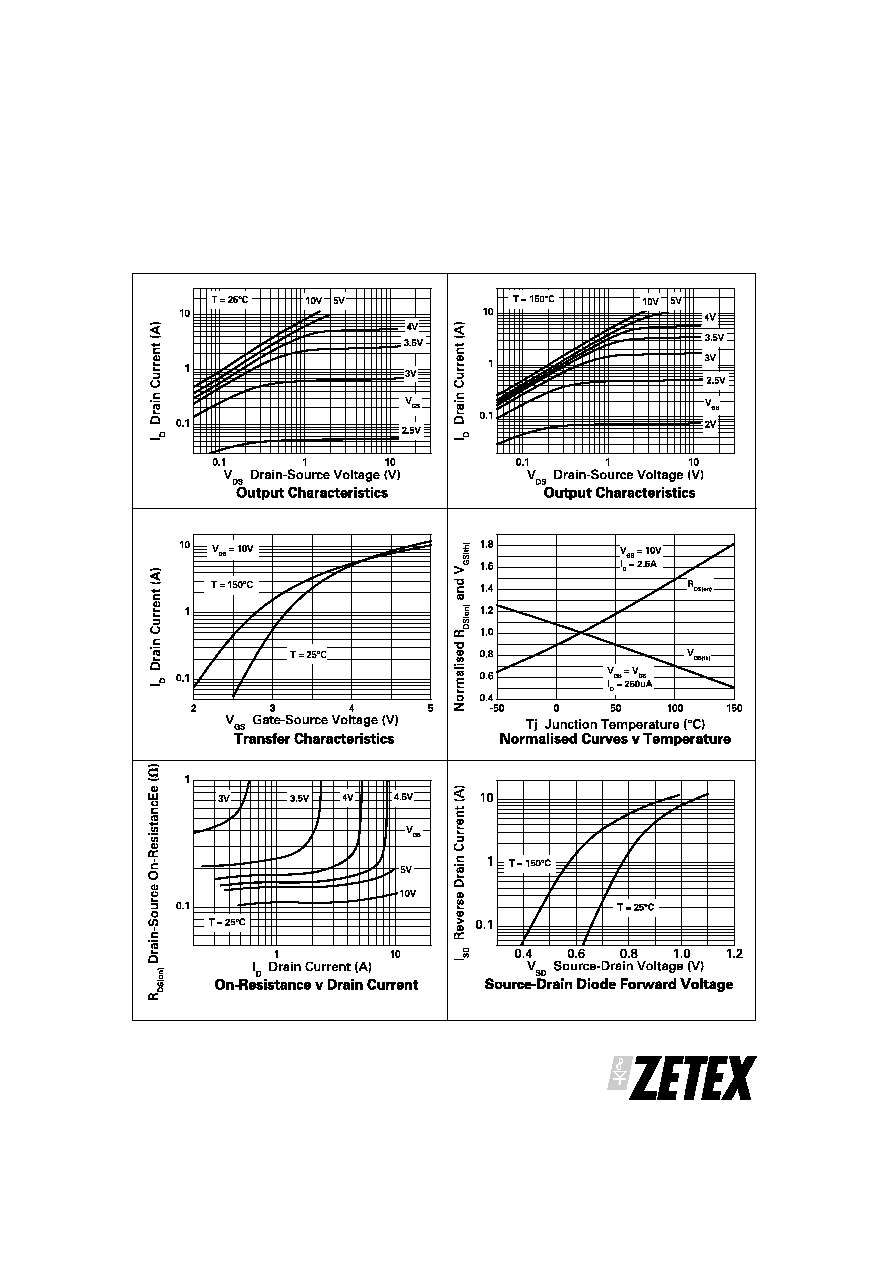
STATIC
Drain-Source Breakdown Voltage
V(BR)DSS
60
V
ID=250 A, VGS=0V
Zero Gate Voltage Drain Current
IDSS
1
A
VDS=60V, VGS=0V
Gate-Body Leakage
IGSS
100
nA
VGS=
±
20V, VDS=0V
Gate-Source Threshold Voltage
VGS(th)
1.0
V
I
D
=250 A, VDS= VGS
Static Drain-Source On-State
Resistance (1)
RDS(on)
0.140
0.250
VGS=10V, ID=4.4A
VGS=4.5V, ID=3.8A
Forward Transconductance (3)
gfs
4.9
S
VDS=15V,ID=2.5A
DYNAMIC (3)
Input Capacitance
Ciss
330
pF
VDS=40 V, VGS=0V,
f=1MHz
Output Capacitance
Coss
35.2
pF
Reverse Transfer Capacitance
Crss
17.1
pF
SWITCHING(2) (3)
Turn-On Delay Time
td(on)
1.95
ns
VDD =30V, ID=2.5A
RG=6.0 , VGS=10V
(refer to test circuit)
Rise Time
tr
3.5
ns
Turn-Off Delay Time
td(off)
8.2
ns
Fall Time
tf
4.6
ns
Gate Charge
Qg
3.0
nC
VDS=15V, VGS=5V,
ID=2.5A
Total Gate Charge
Qg
5.7
nC
VDS=15V,VGS=10V,
I
D
=2.5A
(refer to test circuit)
Gate-Source Charge
Qgs
1.25
nC
Gate-Drain Charge
Qgd
0.86
nC
SOURCE-DRAIN DIODE
Diode Forward Voltage (1)
VSD
0.85
0.95
V
TJ=25∞C, IS=2.8A,
VGS=0V
Reverse Recovery Time (3)
trr
21.5
ns
TJ=25∞C, IF=2.5A,
di/dt= 100A/
µ
s
Reverse Recovery Charge (3)
Qrr
20.5
nC
ELECTRICAL CHARACTERISTICS (at TA = 25∞C unless otherwise stated)
NOTES
(1) Measured under pulsed conditions. Width
300
µ
s. Duty cycle
2% .
(2) Switching characteristics are independent of operating junction temperature.
(3) For design aid only, not subject to production testing.