S E M I C O N D U C T O R S
DESCRIPTION
The ZXSC440 is a dedicated photoflash charger,
charging an 80 F photoflash capacitor to 300V in 3.5
seconds from a 3V supply.
The flyback conversion efficiency is typically 75%,
much higher than the commonly used discrete
charging circuits.
The Charge pin enables the circuit to be initiated from
the camera's microprocessor, using negligible current
when flash is not being used.
FEATURES
∑
Charges a 80 F photoflash capacitor to 300V in
3.5 seconds from 3V
∑
Charges various value photoflash capacitors
∑
Over 75% flyback efficiency
∑
Charge and Ready pins
∑
Consumes only 4.5 A when not charging
∑
Small MSOP8 low profile package
The Ready pin signals the microprocessor when the
flash is charged and ready to be fired.
A small amount of hysteresis on the voltage feedback
shuts down the device as long as the capacitor remains
fully charged, again using negligible current.
APPLICATIONS
∑
Digital camera flash unit
∑
Film camera flash unit
ZXSC440
DRAFT ISSUE F - MAY 2004
PHOTOFLASH CHARGER
1
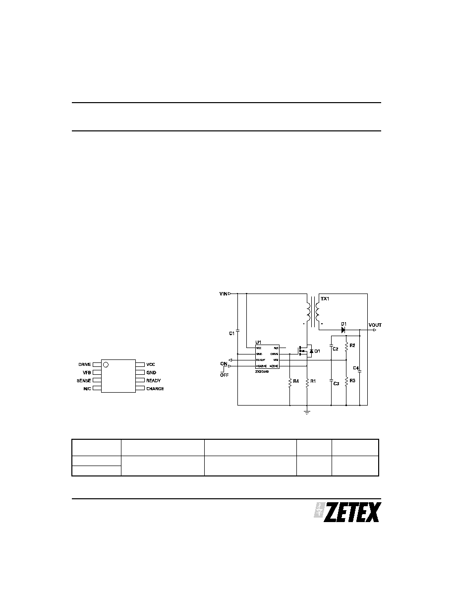
PINOUT
MSOP8 pin TOP VIEW
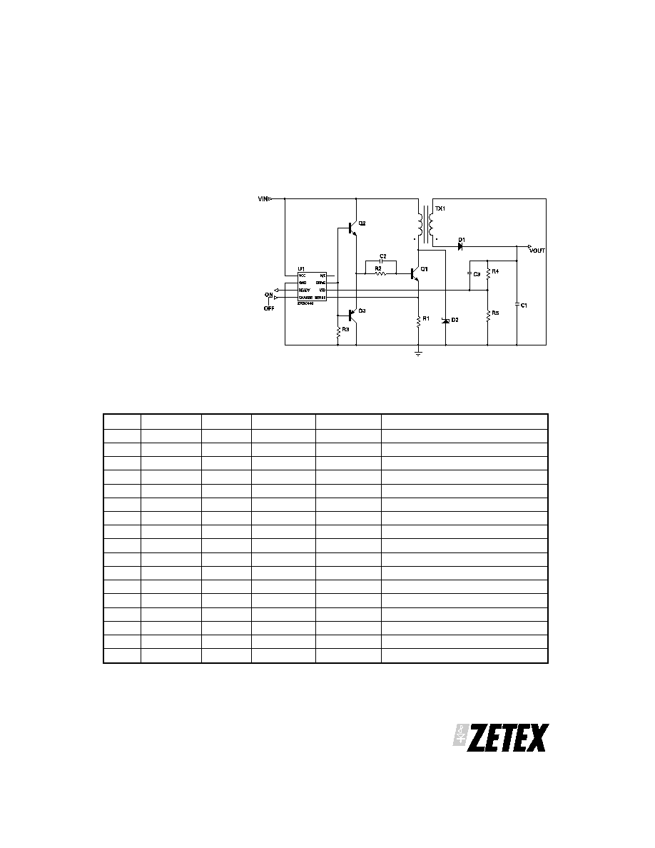
TYPICAL APPLICATION CIRCUIT
DEVICE
DEVICE DESCRIPTION
TEMPERATURE RANGE
PART
MARK
TAPING
OPTIONS
ZXSC440X8TA
Camera flash charger
-40∞C to +85∞C
ZXSC440
TA, TC
ZXSC440X8TC
ORDERING INFORMATION
∑
TA reels hold 1000 devices
∑
TC reels hold 4000 devices
ZXSC440
S E M I C O N D U C T O R S
DRAFT ISSUE F - MAY 2004
2
PARAMETER
LIMIT
UNIT
V
CC
-0.3 to +10
V
DRIVE
-0.3 to V
CC
+ 0.3
V
READY
-0.3 to V
CC
+ 0.3
V
CHARGE
-0.3 to The lower of (+5.0) or (V
CC
+0.3)
V
V
FB
, SENSE
-0.3 to The lower of (+5.0) or (V
CC
+0.3)
V
Operating temperature
-40 to +85
∞C
Storage temperature
-55 to +150
∞C
Power dissipation at 25∞C
450
mW
ABSOLUTE MAXIMUM RATINGS
SYMBOL
PARAMETER
CONDITIONS
MIN.
TYP.
MAX.
UNIT
V
CC
V
CC
range
1.8
8
V
Iq
(1)
Quiescent current
V
CC
=8V
220
A
I
STDN
Shutdown current
4.5
A
Eff
(2)
Efficiency
85
%
Acc
REF
Reference tolerance
1.8V < V
CC
< 8V
-3.0
3.0
%
TCO
REF
Reference temp co
0.005
%/∞C
T
DRV
Discharge pulse width
1.8V < V
CC
< 8V
1.7
s
F
OSC
Operating frequency
200
kHz
INPUT PARAMETERS
V
SENSE
Sense voltage
22
28
34
mV
I
SENSE
Sense input current
V
FB
=0V;V
SENSE
=0V
-1
-7
-15
A
V
FB
Feedback voltage
291
300
309
mV
I
FB
(2)
Feedback input current
V
FB
=0V;V
SENSE
=0V
-1.2
-4.5
A
VIH
(3)
Shutdown threshold
1.5
V
CC
V
VIL
Shutdown threshold
0
0.55
V
dV
LN
Line voltage regulation
0.5
%/V
OUTPUT PARAMETERS
I
DRIVE
Transistor drive current
V
DRIVE
= 0.7V
2
3.4
5
mA
V
DRIVE
Transistor voltage drive
0
V
CC
-0.4
V
C
DRIVE
Mosfet gate drive cpbty
300
pF
VOH
READY
Ready flag output high
I
EOR
= -300nA, T
A
=25∞C
2.5
V
CC
V
VOL
READY
Ready flag output low
I
EOR
= 1mA, T
A
=25∞C
0
1
V
T
READY
T
A
=25∞C
195
s
dI
LD
Load current regulation
0.01
%/mA
ELECTRICAL CHARACTERISTICS
(Test conditions V
CC
= 3V, T= 25∞C unless otherwise stated)
NOTES
(1) Excluding gate/base drive current.
(2) IFB is typically half of these at 3V.
(3) Shutdown pin voltage must not exceed (VCC+0.3V) or 5V, whichever is lower.
ZXSC440
S E M I C O N D U C T O R S
DRAFT ISSUE F - MAY 2004
3
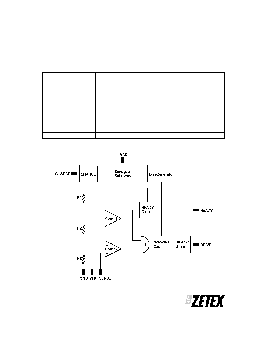
BLOCK DIAGRAM
PIN #
NAME
DESCRIPTION
1
DRIVE
Drive output for external switching transistor. Connect to base or gate of external
switching transistor
2
V
FB
Reference voltage. Internal threshold set to 300mV. Connect external resistor
network to set output voltage
3
SENSE
Inductor current sense input. Internal threshold voltage set to 28mV. Connect
external sense resistor
4
N/C
5
CHARGE
Initiate photoflash capacitor charging
6
READY
Signal to microprocessor when photoflash capacitor charged
7
GND
Ground
8
V
CC
Supply voltage, 1.8V to 8V
ABSOLUTE MAXIMUM RATINGS

DEVICE DESCRIPTION
Bandgap reference
All threshold voltages and internal currents are derived
from a temperature compensated bandgap reference
circuit with a reference voltage of 1.22V nominal. If the
REF terminal is used as a reference for external
devices, the maximum load should not exceed ±2 A.
Dynamic drive output
Depending on the input signal, the output is either
"LOW" or "HIGH". In the high state a 3.4mA current
source (max drive voltage = V
CC
-0.4V) drives the base
or gate of the external transistor. In order to operate the
external switching transistor at optimum efficiency,
both output states are initiated with a short transient
current in order to quickly discharge the base or the
gate of the switching transistor.
Switching circuit
The switching circuit consists of two comparators,
Comp1 and Comp2, a gate U1, a monostable and the
drive output. Normally the DRIVE output is "HIGH"; the
external switching transistor is turned on. Current
ramps up in the inductor, the switching transistor and
external current sensing resistor. This voltage is
sensed by comparator, Comp2, at input SENSE. Once
the current sense voltage across the sensing resistor
exceeds 28mV, comparator, Comp2, through gate U1,
triggers a re-triggerable monostable and turns off the
output drive stage for 1.7 s. The inductor discharges
into the reservoir capacitor. After 1.7 s a new charge
cycle begins, thus ramping the output voltage. When
the output voltage reaches the nominal value and V
FB
gets an input voltage of more than 300mV, the
monostable is forced "on" from Comp1 through gate
U1, until the feedback voltage falls below 300mV. The
above action continues to maintain regulation, with
slight hysteresis on the feedback threshold.
READY detector
T h e R E A D Y c i r c u i t i s a r e - t r i g g e r a b l e 1 9 5 s
monostable, which is re-triggered by every down
regulating action of comparator Comp1. As long as
regulation takes place, output READY is "HIGH" (high
impedance, 100K to V
CC
). Short dips of the output
voltage of less than 195 s are ignored. If the output
voltage falls below the nominal value for more than
195 s, output READY goes "LOW". This can be used to
signal to the camera controller that the flash unit has
charged fully and is ready to use.
ZXSC440
S E M I C O N D U C T O R S
DRAFT ISSUE F - MAY 2004
4
ZXSC440
S E M I C O N D U C T O R S
DRAFT ISSUE F - MAY 2004
5
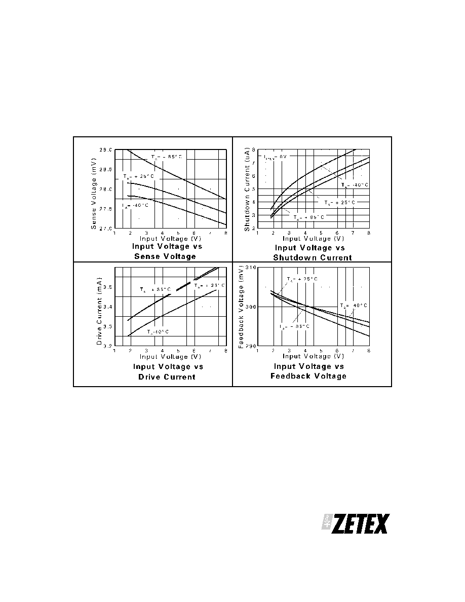
TYPICAL OPERATING CHARACTERISTICS
(For typical application circuit at V
IN
=3V and T
A
=25 ∞C unless otherwise stated)
APPLICATIONS
Switching transistor selection
The choice of switching transistor has a major impact
on the converter efficiency. For optimum performance,
a bipolar transistor with low V
CE(SAT)
and high gain is
required. The V
CEO
of the switching transistor is also an
important parameter as this sees typically three times
the input voltage when the transistor is switched off.
Zetex SuperSOT
TM transistors are an ideal choice for
this application. At input voltages above 4V, suitable
Zetex MOSFET transistors will give almost the same
performance with a simpler drive circuit, omitting the
ZXTD6717 pre-drive stage.
Using a MOSFET, the
Schottky diode may be omitted, as the body diode of
the MOSFET will perform the same function, with just a
small loss of efficiency.
Output rectifier diode selection
The diode should have a fast recovery, as any time
spent in reverse conduction removes energy from the
reservoir capacitor and dumps it, via the transformer,
into the protection diode across the output transistor.
This seriously reduces efficiency. Two BAS21 diodes
in series have been used, bearing in mind that the
reverse voltage across the diode is the sum of the
output voltage together with the input voltage
multiplied by the step-up ratio of the transformer:
V
R(DIODE)
= V
OUT(MAX)
+ (V
IN
x T
URNS
R
ATIO
)
Sense resistor
A low value sense resistor is required to set the peak
current. Power in this resistor is negligible due to the
low sense voltage threshold, V
SENSE
. Below is a table of
recommended sense resistors:
Using a 22m
sense resistor results in a peak current of
just over 1.2A.
Therefore, with a 300V output, a supply of 8 volts and a
1:12 step-up transformer, there will be a 396V across
the diode. This occurs during the current ramp-up in
the primary, as it transforms the input voltage up by the
turns ratio and the polarity at the secondary is such as
to
add
to the output voltage already being held off by
the diode.
Peak current definition
In general, the I
PK
value must be chosen to ensure that
the switching transistor, Q1, is in full saturation with
maximum output power conditions, assuming
worse-case input voltage and transistor gain under all
operating temperature extremes.
Once I
PK
is decided the value of R
SENSE
can be
determined by:
R
V
I
SENSE
SENSE
PK
=
ZXSC440
S E M I C O N D U C T O R S
DRAFT ISSUE F - MAY 2004
6
Manufacturer
Series
R
DC
(
) Range
Size
Tolerance
URL
Cyntec
RL1220
0.022 - 10
0805
±5%
http://www.cyntec.com
IRC
LR1206
0.010 - 1.0
1206
±5%
http://www.irctt.com
Transformer parameters
Proprietary transformers are available, for example the
Pulse PAO367, Primary inductance: 24uH, Core: Pulse
PAO367, Turns ratio: 1:12, see Bill of Materials below. If
designing a transformer, bear in mind that the primary
current may be over an amp and, if this flows through
10 turns, the primary flux will be 10 Amp. Turns and
small cores will need an air gap to cope with this value
without saturation.
Secondary winding capacitance
should not be too high as this is working at 300V and
could soon cause excessive losses.
ZXSC440
S E M I C O N D U C T O R S
DRAFT ISSUE F - MAY 2004
7
Part No.
Size
(WxLxH) mm
L
PRI
( H)
L
PRI -LEAK
(nH)
N
R
PRI
(m )
R
SEC
( )
Manufacturer
T-15-089
6.4x7.7x4
12
400
10:2
211
27
Tokyo Coil Eng.
www.tokyo-coil.co.jp
T-15-083
8x8.9x2
20
500
10:2
675
35
SBL-5.6-1
5.6x8.5x4
10
200
10:2
103
26
Kijima Musen
Kijimahk@netvigator.com
PAO367
9.1x9.1x5.1
24
12:1
Pulse
www.pulseeng.com
ZXSC440 Transformer specifications
Output power calculation
This is approximately the power stored in the coil times
the frequency of operation times the efficiency.
Assuming a current of 1.2 amps in a 30µH primary, the
stored energy will be 21.6µJ. The frequency is set by
the time it takes the primary to reach 1.2 amps plus the
1.7µs time allowed to discharge the energy into the
reservoir capacitor. Using 3 volts, the ramp time is
12µs, so the frequency will be 73kHz, giving an input
power of about 1.6 watts. With an efficiency of 75% the
output power will be 1.2 watts.
An 80µF capacitor
charged to 300 volts stores 3.6J, so 1.2 watts will take 3
seconds to charge it. Higher input voltages reduce the
ramp time, the frequency therefore goes up and the
output power is increased, resulting in shorter
charging times.
Output voltage adjustment
The ZXSC440 are adjustable output converters
allowing the end user the maximum flexibility. For
adjustable operation a potential divider network is
connected as follows:
The output voltage is determined by the equation:
V
OUT
= V
FB
(1 + RA / RB),
where V
FB
=300mV
In a circuit giving 300 volts, the "1" in the above
equation becomes negligible compared to the ratio
which is around 1000.
It will not be exactly
1000because of the negative input current in the
feedback pin. The resistor values, RA and RB, should
be maximized to improve efficiency and decrease
battery drain. Optimization can be achieved by
providing a minimum current of I
FB(MAX)
=200nA to the
V
FB
pin. Output is adjustable from V
FB
to the (BR)V
CEO
of the switching transistor, Q1.
In practice, there will be some stray capacitance across
RA and this will cause a lead in the feedback which can
affect hysteresis (it makes the device shut down too
early) and it is best to swamp this with a capacitor CA
and then use a capacitor CB across RB where CB/CA =
RA/RB.
This is similar to the method used for
compensating oscilloscope probes.
ZXSC440
S E M I C O N D U C T O R S
DRAFT ISSUE F - MAY 2004
8

Layout issues
Layout is critical for the circuit to function in the most
efficient manner in terms of electrical efficiency,
thermal considerations and noise.
For 'step-up converters' there are four main current
loops, the input loop, power-switch loop, rectifier loop
and output loop. The supply charging the input
capacitor forms the input loop. The power-switch loop
is defined when Q1 is 'on', current flows from the input
through the transformer primary, Q1, R
SENSE
and to
ground. When Q1 is 'off', the energy stored in the
transformer is transferred from the secondary to the
output capacitor and load via D1, forming the rectifier
loop. The output loop is formed by the output capacitor
supplying the load when Q1 is switched back off.
To optimize for best performance each of these loops
kept separate from each other and interconnected with
short, thick traces thus minimizing parasitic
inductance, capacitance and resistance. Also the
R
SENSE
resistor should be connected, with minimum
trace length, between emitter lead of Q1 and ground,
again minimizing stray parasitics.
ZXSC440
S E M I C O N D U C T O R S
DRAFT ISSUE F - MAY 2004
9
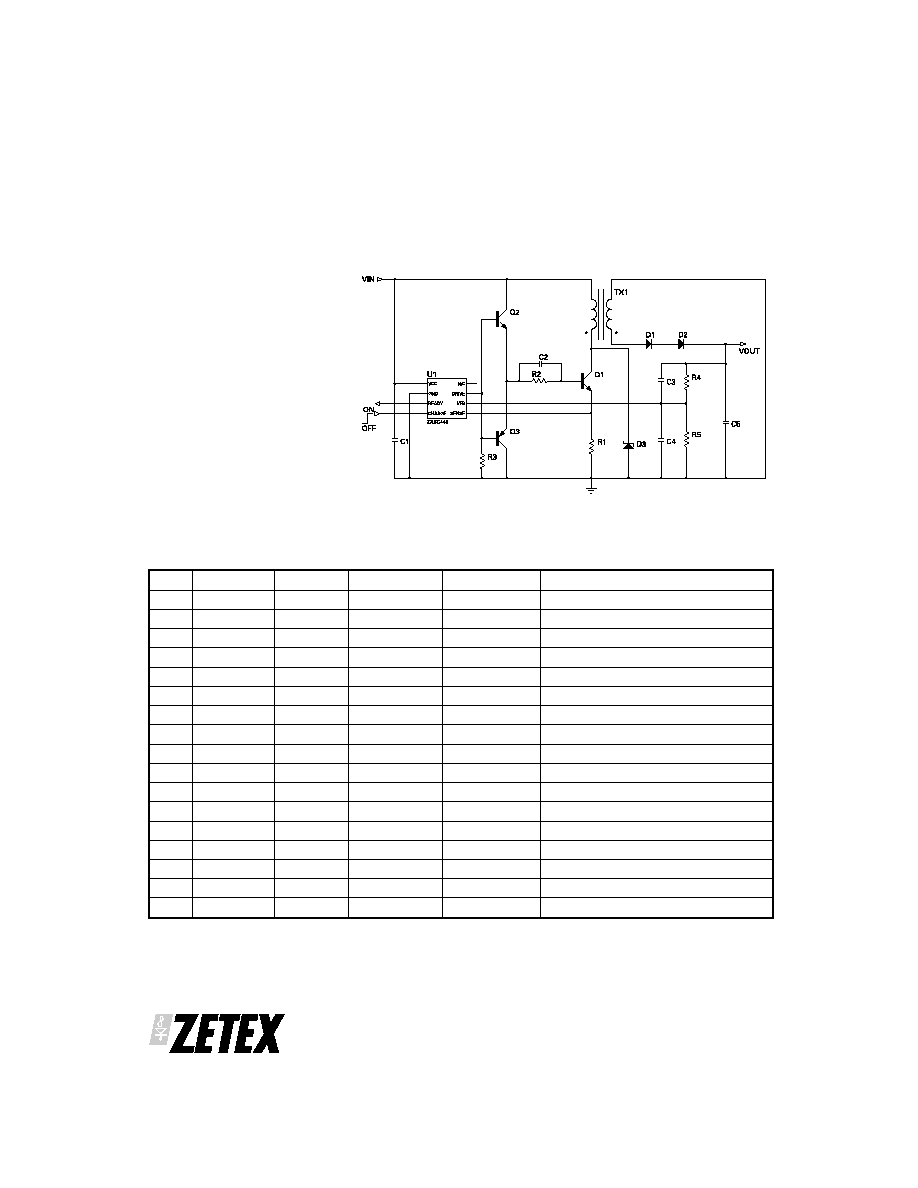
REFERENCE DESIGNS
General camera photoflash charger
Specification
V
IN
=
5V
V
OUT
=
275V
Efficiency =
71%
Charging time =
4 seconds
ZXSC440
S E M I C O N D U C T O R S
DRAFT ISSUE F - MAY 2004
10
Circuit diagram
Ref
Value
Package
Part number
Manufacturer
Notes
U1
MSOP8
ZXSC440
Zetex
Q1
SOT23
ZXMN6A07F
Zetex
60V N-channel MOSFET
D1
(2)
200V
SOT23
BAS21
Philips
x2 200V fast rectifier diodes
connected in series
Tx1
Pulse
See note
(1)
R1
22m
0805
RL1210
Cyntec
R2
10M /400V
Axial
Generic
Generic
Output voltage across resistor
R3
10k
0805
Generic
Generic
R4
100k
0805
Generic
Generic
C1
100uF/10V
0805
Generic
Murata
C2
10pF/500V
1206
Generic
Generic
Output voltage seen across capacitor
C3
10nF/6V3
1206
Generic
Generic
C4
120uF/330V
Radial
FW Series
Rubycon
Photoflash capacitor
Bill of materials
NOTES:
(1) Transformer specification: Primary inductance: 24uH, Core: Pulse PAO367, Turns ratio: 1:12
(2) Two BAS21 200V rectifier diodes are connected in series and used in place of a 400V rectifier diode to provide faster switching speeds and
higher efficiency.
High power digital camera photoflash charger
Specification
V
IN
=
3V
V
OUT
=
275V
Efficiency =
69%
Charging time =
5 seconds
ZXSC440
S E M I C O N D U C T O R S
DRAFT ISSUE F - MAY 2004
11
Circuit diagram
Ref
Value
Package
Part number
Manufacturer
Notes
U1
MSOP8
ZXSC440
Zetex
U2
SOT23-6
ZXTD6717
Zetex
NPN/PNP dual
Q1
SOT23
FMMT619
Zetex
50V NPN low sat
D1
200V
SOT23
BAS21
Philips
200V fast rectifier
D2
200V
SOT23
BAS21
Philips
200V fast rectifier
D3
2A
SOT23-6
ZLLS2000
Zetex
2A Schottky diode
Tx1
PAO367
Pulse
See note
(1)
R1
22m
0805
RL1210
Cyntec
R2
130
0805
Generic
Generic
R3
2k2
0805
Generic
Generic
R4
10M /400V
Axial
Generic
Generic
Output voltage across resistor
R5
10k
0805
Generic
Generic
C1
100uF/10V
0805
Generic
Murata
C2
220nF
0805
GRM Series
Murata
C3
10pF/500V
1206
Generic
Generic
Output voltage seen across capacitor
C4
10nF/6V3
1206
Generic
Generic
C5
120uF/330V
Radial
FW Series
Rubycon
Photoflash capacitor
Bill of materials
NOTES:
(1) Transformer specification: Primary inductance: 24uH, Core: Pulse PAO367, Turns ratio: 1:12
Low power digital camera photoflash charger
Specification
V
IN
=
3V
V
OUT
=
275V
Efficiency =
58%
Charging time =
6.8 seconds
ZXSC440
S E M I C O N D U C T O R S
DRAFT ISSUE F - MAY 2004
12
Circuit diagram
Ref
Value
Package
Part number
Manufacturer
Notes
U1
MSOP8
ZXSC440
Zetex
U2
SOT23-6
ZXTD6717
Zetex
NPN/PNP dual
Q1
SOT23
FMMT619
Zetex
50V NPN low sat
D1
200V
SOT23
BAS21
Philips
200V fast rectifier
D2
200V
SOT23
BAS21
Philips
200V fast rectifier
D3
2A
SOT23-6
ZLLS2000
Zetex
2A Schottky diode
Tx1
Sumida
See note
(1)
R1
33m
0805
RL1210
Cyntec
R2
200
0805
Generic
Generic
R3
2k2
0805
Generic
Generic
R4
10M /400V
Axial
Generic
Generic
Output voltage across resistor
R5
10k
0805
Generic
Generic
C1
100uF/10V
0805
Generic
Murata
C2
220nF
0805
GRM Series
Murata
C3
10pF/500V
1206
Generic
Generic
Output voltage seen across capacitor
C4
10nF/6V3
1206
Generic
Generic
C5
80uF/330V
Radial
FW Series
Rubycon
Photoflash capacitor
Bill of materials
NOTES:
(1) Transformer specification: Primary inductance: 32uH, Core: Sumida CEEH64, Turns ratio: 1:10
ZXSC440
S E M I C O N D U C T O R S
DRAFT ISSUE F - MAY 2004
13
Europe
Zetex GmbH
Streitfeldstraþe 19
D-81673 M¸nchen
Germany
Telefon: (49) 89 45 49 49 0
Fax: (49) 89 45 49 49 49
europe.sales@zetex.com
Americas
Zetex Inc
700 Veterans Memorial Hwy
Hauppauge, NY 11788
USA
Telephone: (1) 631 360 2222
Fax: (1) 631 360 8222
usa.sales@zetex.com
Asia Pacific
Zetex (Asia) Ltd
3701-04 Metroplaza Tower 1
Hing Fong Road, Kwai Fong
Hong Kong
Telephone: (852) 26100 611
Fax: (852) 24250 494
asia.sales@zetex.com
Corporate Headquaters
Zetex plc
Fields New Road, Chadderton
Oldham, OL9 8NP
United Kingdom
Telephone (44) 161 622 4444
Fax: (44) 161 622 4446
hq@zetex.com
These offices are supported by agents and distributors in major countries world-wide.
This publication is issued to provide outline information only which (unless agreed by the Company in writing) may not be used, applied or reproduced
for any purpose or form part of any order or contract or be regarded as a representation relating to the products or services concerned. The Company
reserves the right to alter without notice the specification, design, price or conditions of supply of any product or service.
For the latest product information, log on to
www.zetex.com
© Zetex plc 2004
DIM
Millimeters
Inches
DIM
Millimeters
Inches
Min
Max
Min
Max
Min
Max
Min
Max
A
-
1.10
-
0.0433
E
4.90 BSC
0.025 BSC
A1
0.05
0.15
0.002
0.006
E1
2.90
3.10
0.114
0.122
A2
0.75
0.95
0.0295
0.0374
e
0.65 BSC
0.193 BSC
b
0.25
0.40
0.010
0.0157
L
0.40
0.70
0.0157
0.0192
c
0.13
0.23
0.005
0.009
R
0.07
-
0.0027
-
PACKAGE DIMENSIONS
Controlling dimensions are in millimeters. Approximate conversions are given in inches
E
E1
e
D
A
A1
A2
L
0.25
15%%D MAX
GAGE PLANE
R1
R
c
INDENT AREA
(D/2 X E1/2)
b
0%%D-6%%D
1
8
PACKAGE OUTLINE