Issue 2 - January 2006
1
www.zetex.com
© Zetex Semiconductors plc 2006
ZXTN2031F
50V, SOT23, NPN medium power transistor
Summary
V
(BR)CEV
> 80V, V
(BR)CEO
> 50V
I
C(cont)
= 5A
R
CE(sat)
= 24m typical
V
CE(sat)
< 40mV @ 1A
P
D
= 1.2W
Complementary part number: ZXTP2025F
Description
Advanced process capability and package design have been used to
maximize the power handling and performance of this small outline
transistor. The compact size and ratings of this device make it ideally
suited to applications where space is at a premium.
Feature
∑
Higher power dissipation SOT23 Package
∑
High peak current
∑
Low saturation voltage
∑
High gain
∑
80V forward blocking voltage
Applications
∑
MOSFET and IGBT gate driving
∑
Motor drive
∑
Relay, lamp and solenoid drive
∑
DC-DC converters
Ordering information
Device marking
322
Device
Reel size
(inches)
Tape width
(mm)
Quantity per reel
ZXTN2031FTA
7
8
3,000
Pinout - top view
ZXTN2031F
Issue 2 - January 2006
2
www.zetex.com
© Zetex Semiconductors plc 2006
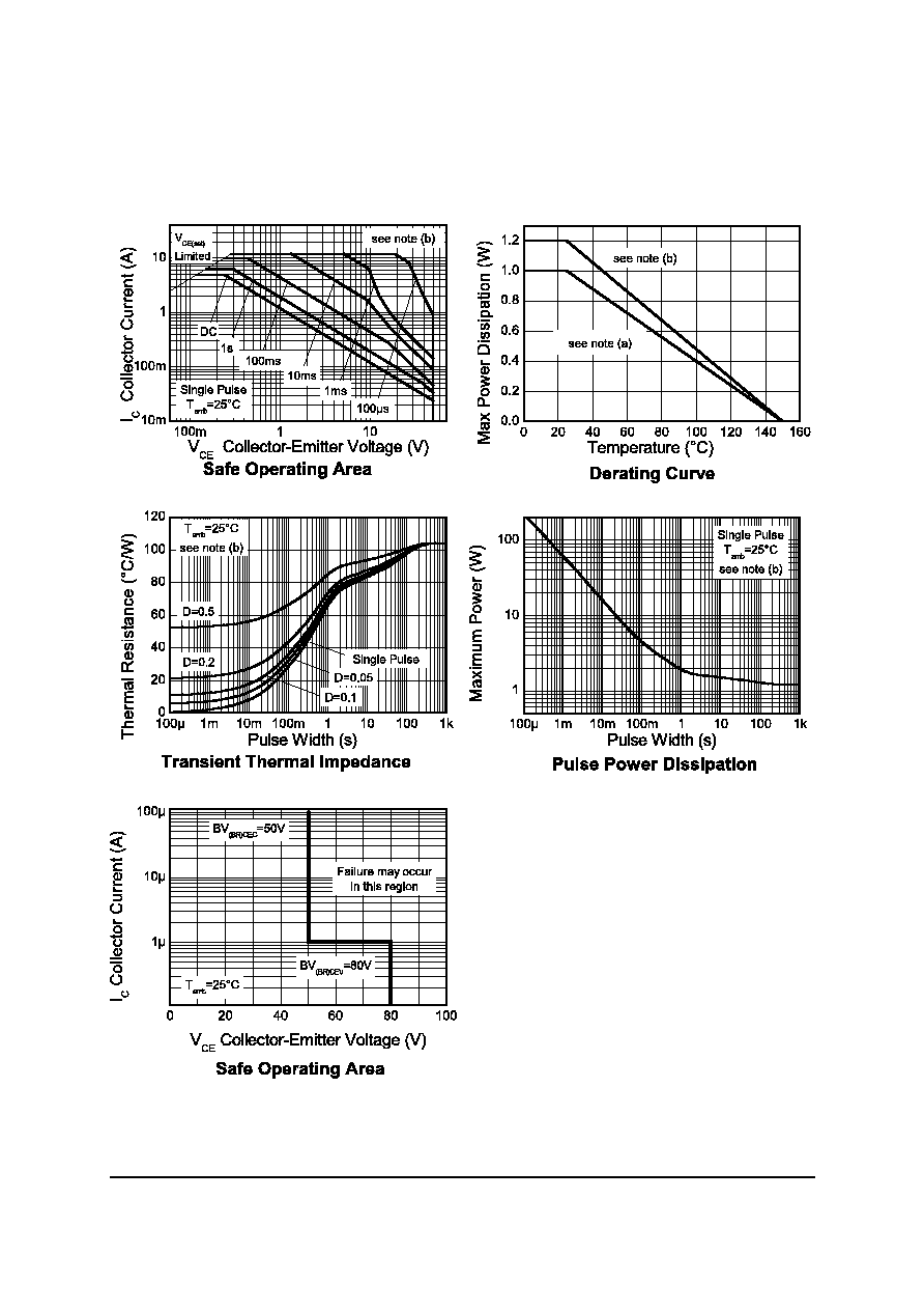
Absolute maximum ratings
Thermal resistance
Parameter
Symbol
Limit
Unit
Collector-base voltage
V
CBO
80
V
Collector-emitter voltage
V
(BR)CEV
80
V
Collector-emitter voltage
V
CEO
50
V
Emitter-base voltage
V
EBO
7.0
V
Peak pulse current
I
CM
12
A
Continuous collector current
(a)
I
C
5
A
Base current
I
B
1.2
A
Power dissipation @ T
A
=25
o
C
(a)
Linear derating factor
P
D
1.0
8.0
W
mW/
o
C
Power dissipation @ T
A
=25
o
C
(b)
Linear derating factor
P
D
1.2
9.6
W
mW/
o
C
Power dissipation @ T
A
=25
o
C
(c)
Linear derating factor
P
D
1.56
12.5
W
mW/
o
C
Operating and storage temperature
T
j
:T
stg
-55 to
+150
o
C
Parameter
Symbol
Value
Unit
Junction to ambient
(a)
NOTES:
(a) Mounted on 18mm x 18mm x 1.6mm FR4 PCB with a very high coverage of 2 oz weight copper in still air conditions.
R
JA
125
o
C/W
Junction to ambient
(b)
(b) Mounted on 30mm x 30mm x 1.6mm FR4 PCB with a very high coverage of 2 oz weight copper in still air conditions.
R
JA
104
o
C/W
Junction to ambient
(c)
(c) As (b) above measured at t<5secs.
R
JA
80
o
C/W
ZXTN2031F
Issue 2 - January 2006
4
www.zetex.com
© Zetex Semiconductors plc 2006
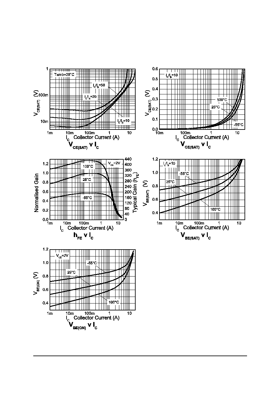
Electrical characteristics (at T
amb
= 25∞C unless otherwise stated)
Parameter
Symbol
Min.
Typ.
Max.
Unit
Conditions
Collector-base breakdown
voltage
V
(BR)CBO
80
175
V
I
C
=100
µA
Collector-emitter breakdown
voltage
V
(BR)CEV
80
175
V
I
C
=1
µA, -1V< V
BE
<+0.3V
Collector-emitter breakdown
voltage
V
(BR)CEO
50
75
V
I
C
=10mA
(a)
NOTES:
(a) Measured under pulsed conditions. Pulse width=300 S. Duty cycle 2%.
Emitter-base breakdown
voltage
V
(BR)EBO
7.0
8.3
V
I
E
=100
µA
Collector-emitter cut-off
current
I
CEV
<1
20
nA
V
CE
=60V, V
BE
= -1V
Collector-base cut-off current I
CBO
<1
20
nA
V
CB
=60V
Emitter-base cut-off current
I
EBO
<1
10
nA
V
EB
=6V
Static forward current
transfer ratio
H
FE
190
200
200
80
300
350
340
125
560
I
C
=10mA, V
CE
=2V
(a)
I
C
=500mA, V
CE
=2V
(a)
I
C
=2A, V
CE
=2V
(a)
I
C
=5A, V
CE
=2V
(a)
Collector-emitter saturation
voltage
V
CE(sat)
13
30
80
135
18
40
110
170
mV
mV
mV
mV
I
C
=0.1A, I
B
=5mA
(a)
I
C
=1A, I
B
=100mA
(a)
I
C
=2A, I
B
=40mA
(a)
I
C
=5A, I
B
=250mA
(a)
Base-emitter saturation
voltage
V
BE(sat)
0.80
0.92
0.90
1.00
V
V
I
C
=2A, I
B
=40mA
(a)
I
C
=5A, I
B
=250mA
(a)
Base-emitter turn-on voltage
V
BE(on)
0.83
0.93
V
I
C
=5A, V
CE
=2V
(a)
Transition frequency
f
T
125
MHz
Ic=500mA, V
CE
=10V,
f=50MHz
Output capacitance
C
obo
29
pF
V
CB
=10V, f=1MHz
Delay time
t
(d)
16
ns
Rise time
t
(r)
27
ns
V
CC
=12V, I
C
=2.5A,
Storage time
t
(stg)
468
ns
I
B1
=I
B2
=125mA
Fall time
t
(f)
44
ns