1
S E M I C O N D U C T O R S
SUMMARY
BV
CEO
= -40V : R
SAT
= 29m ; I
C
= -5.5A
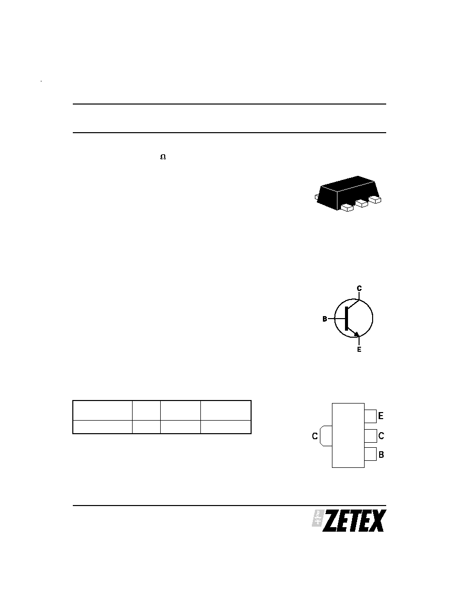
DESCRIPTION
Packaged in the SOT89 outline this new low saturation 40V PNP transistor
offers low on state losses making it ideal for use in DC-DC circuits, line
switching and various driving and power management functions.
FEATURES
∑
Extremely low equivalent on-resistance
∑
5.5 amps continuous current
∑
Up to 15 amps peak current
∑
Very low saturation voltages < -60mV @ -1A
APPLICATIONS
∑
DC - DC converters
∑
MOSFET gate drivers
∑
Charging circuits
∑
Power switches
∑
Motor control
DEVICE MARKING
53Z
ZXTP2009Z
ISSUE 1 - JUNE 2005
40V PNP HIGH GAIN LOW SATURATION MEDIUM POWER TRANSISTOR
IN SOT89
DEVICE
REEL
SIZE
TAPE
WIDTH
QUANTITY PER
REEL
ZXTP2009ZTA
7"
12mm
1,000 units
ORDERING INFORMATION
PINOUT
TOP VIEW
SOT89
ZXTP2009Z
S E M I C O N D U C T O R S
ISSUE 1 - JUNE 2005
2
PARAMETER
SYMBOL
VALUE
UNIT
Junction to ambient
(a)
R
JA
139
∞C/W
Junction to ambient
(b)
R
JA
83
∞C/W
Junction to ambient
(c)
R
JA
60
∞C/W
Junction to ambient
(d)
R
JA
42
∞C/W
NOTES
(a) For a device surface mounted on 15mm x 15mm x 1.6mm FR4 PCB with high coverage of single sided 1oz copper, in still air conditions.
(b) For a device surface mounted on 25mm x 25mm x 1.6mm FR4 PCB with high coverage of single sided 1oz copper, in still air conditions.
(c) For a device surface mounted on 50mm x 50mm x 1.6mm FR4 PCB with high coverage of single sided 1oz copper, in still air conditions.
(d) For a device surface mounted on 25mm x 25mm x 1.6mm FR4 PCB measured at t
5 secs.
THERMAL RESISTANCE
PARAMETER
SYMBOL
LIMIT
UNIT
Collector-base voltage
BV
CBO
-50
V
Collector-base voltage
BV
CBS
-50
V
Collector-emitter voltage
BV
CEO
-40
V
Emitter-base voltage
BV
EBO
-7.5
V
Continuous collector current
(b)
I
C
-5.5
A
Peak pulse current
I
CM
-15
A
Power dissipation at T
A
=25∞C
(a)
Linear derating factor
P
D
0.9
7.2
W
mW/∞C
Power dissipation at T
A
=25∞C
(b)
Linear derating factor
P
D
1.5
12
W
mW/∞C
Power dissipation at T
A
=25∞C
(c)
Linear derating factor
P
D
2.1
16.8
W
mW/∞C
Power dissipation at T
A
=25∞C
(d)
Linear derating factor
P
D
3
24
W
mW/∞C
Operating and storage temperature range
T
j
, T
stg
-55 to 150
∞C
ABSOLUTE MAXIMUM RATINGS
ZXTP2009Z
S E M I C O N D U C T O R S
ISSUE 1 - JUNE 2005
3
CHARACTERISTICS
ZXTP2009Z
S E M I C O N D U C T O R S
ISSUE 1 - JUNE 2005
4
PARAMETER
SYMBOL
MIN.
TYP.
MAX.
UNIT CONDITIONS
Collector-base breakdown voltage
BV
CBO
-50
-90
V
I
C
=-100 A
Collector-emitter breakdown voltage
BV
CES
-50
-90
V
I
C
=-100 A
Collector-emitter breakdown voltage
BV
CEO
-40
-58
V
I
C
=-10mA*
Emitter-base breakdown voltage
BV
EBO
-7.5
-8.3
V
I
E
=-100 A
Collector cut-off current
I
CBO
1
-20
nA
V
CB
=-40V
Collector cut-off current
I
CES
1
-20
nA
V
CB
=-32V
Emitter cut-off current
I
EBO
1
-20
nA
V
EB
=-6V
Collector-emitter saturation voltage
V
CE(SAT)
-15
-44
-50
-120
-70
-125
-130
-162
-30
-60
-70
-165
-80
-175
-175
-185
mV
mV
mV
mV
mV
mV
mV
mV
I
C
=-0.1A, I
B
=-10mA*
I
C
=-1A, I
B
=-100mA*
I
C
=-1A, I
B
=-50mA*
I
C
=-1A, I
B
=-10mA*
I
C
=-2A, I
B
=-200mA*
I
C
=-2A, I
B
=-40mA*
I
C
=-3.5A, I
B
=-175mA*
I
C
=-5.5A, I
B
=-550mA*
Base-emitter saturation voltage
V
BE(SAT)
-820
-1000
-900
-1075
mV
mV
I
C
=-2A, I
B
=-40mA*
I
C
=-5.5A, I
B
=-550mA*
Base-emitter turn-on voltage
V
BE(ON)
-778
-869
-850
-950
mV
mV
I
C
=-2A, V
CE
=-2V*
I
C
=-5.5A, V
CE
=-2V*
Static forward current transfer ratio
H
FE
200
200
170
110
390
350
290
175
550
I
C
=-10mA, V
CE
=-2V*
I
C
=-0.5A, V
CE
=-2V*
I
C
=-2A, V
CE
=-2V*
I
C
=-5.5A, V
CE
=-2V*
Transition frequency
f
T
152
MHz I
C
=-50mA, V
CE
=-10V
f=100MHz
Output capacitance
C
OBO
53
pF
V
CB
=-10V, f=1MHz*
Switching times
t
d
t
r
t
s
t
r
18
17
325
60
ns
I
C
=-1A, V
CC
=-10V,
I
B1
=I
B2
=-100mA
Switching times
t
d
t
r
t
s
t
r
55
107
264
103
ns
I
C
=-2A, V
CC
=-30V,
I
B1
=I
B2
=-20mA
ELECTRICAL CHARACTERISTICS (at T
amb
= 25∞C unless otherwise stated)
* Measured under pulsed conditions. Pulse width
300 s; duty cycle
2%.

ZXTP2009Z
S E M I C O N D U C T O R S
ISSUE 1 - JUNE 2005
5
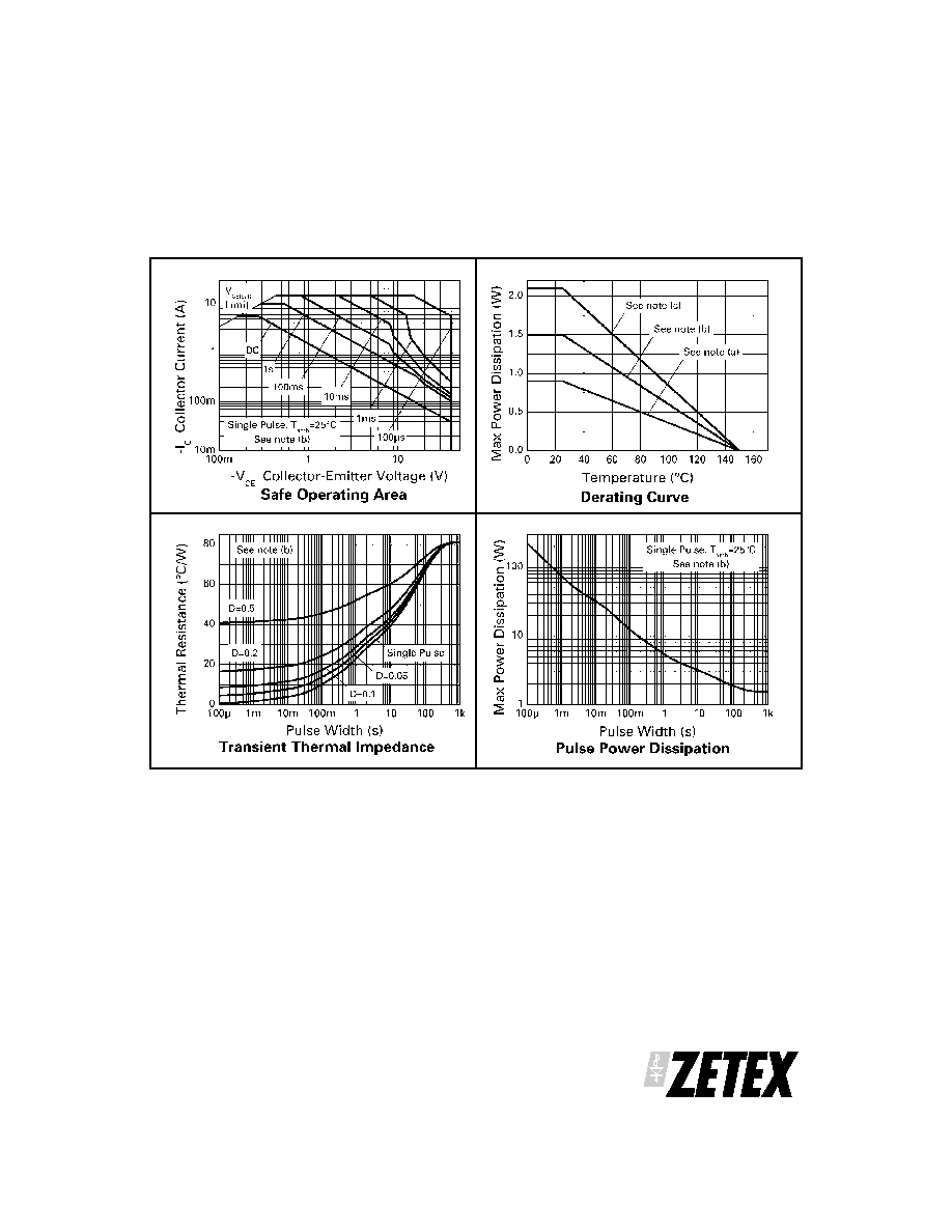
TYPICAL CHARACTERISTICS