
ZiLOG Worldwide Headquarters
∑
532 Race Street
∑
San Jose, CA
95126
Telephone: 408.558.8500
∑
Fax: 408.558.8300
∑
www
.ZiLOG.com
Product Specification
PRELIMINARY
eZ80190
PS006611-0703

PS006611-0703
PRELIMINARY
This publication is subject to replacement by a later edition.
T
o determine whether
a later edition exists, or to request copies of publications, contact:
ZiLOG W
orldwide Headquarters
532 Race Street
San Jose, CA
95126
T
elephone: 408.558.8500
Fax: 408.558.8300
www
.ZiLOG.com
Document Disclaimer
ZiLOG is a registered trademark of ZiLOG Inc. in the United States and in other countries.
All other
products and/or service names mentioned herein may be trademarks of the companies with which
they are associated.
©
2003
by ZiLOG, Inc.
All rights reserved. Information in this publication concerning the devices,
applications, or technology described is intended to suggest possible uses and may be superseded.
ZiLOG, INC. DOES NOT
ASSUME LIABILITY
FOR OR PROVIDE
A
REPRESENT
A
TION OF
ACCURACY
OF
THE INFORMA
TION, DEVICES, OR
TECHNOLOGY
DESCRIBED IN
THIS
DOCUMENT
. ZiLOG
ALSO DOES NOT
ASSUME LIABILITY
FOR INTELLECTUAL
PROPER
TY
INFRINGEMENT
RELA
TED IN
ANY
MANNER
T
O USE OF INFORMA
TION, DEVICES, OR
TECHNOLOGY
DESCRIBED HEREIN OR OTHER
WISE. Except with the express written approval
ZiLOG, use of information, devices, or technology as critical components of life support systems is
not authorized. No licenses or other rights are conveyed, implicitly or otherwise, by this document
under any intellectual property rights.

eZ80190
Product Specification
PS006611-0703
P R E L I M I N A R Y
Table of Contents
iii
T
able of Contents
List of Figures
. . . . . . . . . . . . . . . . . . . . . . . . . . . . . . . . . . . . . . . . . . . . . . . . . . .
vi
List of Tables
. . . . . . . . . . . . . . . . . . . . . . . . . . . . . . . . . . . . . . . . . . . . . . . . . . .
viii
Architectural Overview
. . . . . . . . . . . . . . . . . . . . . . . . . . . . . . . . . . . . . . . . . . . .
1
Features
. . . . . . . . . . . . . . . . . . . . . . . . . . . . . . . . . . . . . . . . . . . . . . . . . . . .
1
Block Diagram
. . . . . . . . . . . . . . . . . . . . . . . . . . . . . . . . . . . . . . . . . . . . . . . .
2
Pin Description
. . . . . . . . . . . . . . . . . . . . . . . . . . . . . . . . . . . . . . . . . . . . . . .
4
Register Map
. . . . . . . . . . . . . . . . . . . . . . . . . . . . . . . . . . . . . . . . . . . . . . . . . . .
22
eZ80
Æ
CPU Core
. . . . . . . . . . . . . . . . . . . . . . . . . . . . . . . . . . . . . . . . . . . . . . . .
30
eZ80
Æ
CPU Core Overview
. . . . . . . . . . . . . . . . . . . . . . . . . . . . . . . . . . . . .
30
eZ80
Æ
CPU Core Features
. . . . . . . . . . . . . . . . . . . . . . . . . . . . . . . . . . . . .
30
Programmable Reload Timers
. . . . . . . . . . . . . . . . . . . . . . . . . . . . . . . . . . . . .
31
Programmable Reload Timers Overview
. . . . . . . . . . . . . . . . . . . . . . . . . .
31
Programmable Reload Timer Operation
. . . . . . . . . . . . . . . . . . . . . . . . . . .
32
Programmable Reload Timer Registers
. . . . . . . . . . . . . . . . . . . . . . . . . . .
34
Watch-Dog Timer
. . . . . . . . . . . . . . . . . . . . . . . . . . . . . . . . . . . . . . . . . . . . . . .
39
Watch-Dog Timer Overview
. . . . . . . . . . . . . . . . . . . . . . . . . . . . . . . . . . . .
39
Watch-Dog Timer Operation
. . . . . . . . . . . . . . . . . . . . . . . . . . . . . . . . . . . .
40
Watch-Dog Timer Registers
. . . . . . . . . . . . . . . . . . . . . . . . . . . . . . . . . . . .
40
General-Purpose Input/Output
. . . . . . . . . . . . . . . . . . . . . . . . . . . . . . . . . . . . .
43
GPIO Overview
. . . . . . . . . . . . . . . . . . . . . . . . . . . . . . . . . . . . . . . . . . . . . .
43
GPIO Operation
. . . . . . . . . . . . . . . . . . . . . . . . . . . . . . . . . . . . . . . . . . . . . .
43
GPIO Interrupts
. . . . . . . . . . . . . . . . . . . . . . . . . . . . . . . . . . . . . . . . . . . . . .
46
GPIO Control Registers
. . . . . . . . . . . . . . . . . . . . . . . . . . . . . . . . . . . . . . . .
47
Chip Selects and Wait States
. . . . . . . . . . . . . . . . . . . . . . . . . . . . . . . . . . . . . .
49
Memory and I/O Chip Selects
. . . . . . . . . . . . . . . . . . . . . . . . . . . . . . . . . . .
49
Memory Chip Select Operation
. . . . . . . . . . . . . . . . . . . . . . . . . . . . . . . . . .
49
I/O Chip Select Operation
. . . . . . . . . . . . . . . . . . . . . . . . . . . . . . . . . . . . . .
52
I/O Chip Select Precaution
. . . . . . . . . . . . . . . . . . . . . . . . . . . . . . . . . . . . . 52
Wait States . . . . . . . . . . . . . . . . . . . . . . . . . . . . . . . . . . . . . . . . . . . . . . . . . 53
Chip Select Registers . . . . . . . . . . . . . . . . . . . . . . . . . . . . . . . . . . . . . . . . . 54
Random Access Memory . . . . . . . . . . . . . . . . . . . . . . . . . . . . . . . . . . . . . . . . . 57
RAM Control Registers . . . . . . . . . . . . . . . . . . . . . . . . . . . . . . . . . . . . . . . . 58
Universal ZiLOG Interface . . . . . . . . . . . . . . . . . . . . . . . . . . . . . . . . . . . . . . . . . 60
Baud Rate Generator . . . . . . . . . . . . . . . . . . . . . . . . . . . . . . . . . . . . . . . . . 61
UZI and BRG Control Registers . . . . . . . . . . . . . . . . . . . . . . . . . . . . . . . . . 62
Universal Asynchronous Receiver/Transmitter . . . . . . . . . . . . . . . . . . . . . . . . . 65

eZ80190 Product Specification
PS006611-0703
P R E L I M I N A R Y
Table of Contents
iv
UART Functional Description . . . . . . . . . . . . . . . . . . . . . . . . . . . . . . . . . . . 66
UART Functions . . . . . . . . . . . . . . . . . . . . . . . . . . . . . . . . . . . . . . . . . . . . . 66
UART Interrupts . . . . . . . . . . . . . . . . . . . . . . . . . . . . . . . . . . . . . . . . . . . . . 68
UART Recommended Usage . . . . . . . . . . . . . . . . . . . . . . . . . . . . . . . . . . . 69
UART Registers . . . . . . . . . . . . . . . . . . . . . . . . . . . . . . . . . . . . . . . . . . . . . 70
Serial Peripheral Interface . . . . . . . . . . . . . . . . . . . . . . . . . . . . . . . . . . . . . . . . . 82
SPI Signals . . . . . . . . . . . . . . . . . . . . . . . . . . . . . . . . . . . . . . . . . . . . . . . . . 82
SPI Functional Description . . . . . . . . . . . . . . . . . . . . . . . . . . . . . . . . . . . . . 84
SPI Flags . . . . . . . . . . . . . . . . . . . . . . . . . . . . . . . . . . . . . . . . . . . . . . . . . . . 86
SPI Registers . . . . . . . . . . . . . . . . . . . . . . . . . . . . . . . . . . . . . . . . . . . . . . . 86
I
2
C Serial I/O Interface . . . . . . . . . . . . . . . . . . . . . . . . . . . . . . . . . . . . . . . . . . . 90
I
2
C General Characteristics . . . . . . . . . . . . . . . . . . . . . . . . . . . . . . . . . . . . . 90
Transferring Data . . . . . . . . . . . . . . . . . . . . . . . . . . . . . . . . . . . . . . . . . . . . 91
Clock Synchronization . . . . . . . . . . . . . . . . . . . . . . . . . . . . . . . . . . . . . . . . . 93
Operating Modes . . . . . . . . . . . . . . . . . . . . . . . . . . . . . . . . . . . . . . . . . . . . . 95
I
2
C Registers . . . . . . . . . . . . . . . . . . . . . . . . . . . . . . . . . . . . . . . . . . . . . . . 102
Multiply-Accumulator . . . . . . . . . . . . . . . . . . . . . . . . . . . . . . . . . . . . . . . . . . . . 111
MACC Overview . . . . . . . . . . . . . . . . . . . . . . . . . . . . . . . . . . . . . . . . . . . . 111
Multiply-Accumulator Basic Operation . . . . . . . . . . . . . . . . . . . . . . . . . . . 112
Software Control of the MACC . . . . . . . . . . . . . . . . . . . . . . . . . . . . . . . . . 113
MACC Dual Bank Operation . . . . . . . . . . . . . . . . . . . . . . . . . . . . . . . . . . . 115
IN_SHIFT and OUT_SHIFT . . . . . . . . . . . . . . . . . . . . . . . . . . . . . . . . . . . 118
Recommended Operation . . . . . . . . . . . . . . . . . . . . . . . . . . . . . . . . . . . . . 121
MACC RAM . . . . . . . . . . . . . . . . . . . . . . . . . . . . . . . . . . . . . . . . . . . . . . . . 122
MACC RAM Address Indexing . . . . . . . . . . . . . . . . . . . . . . . . . . . . . . . . . 122
Multiply-Accumulator Control And Data Registers . . . . . . . . . . . . . . . . . . 125
Interrupt Controller . . . . . . . . . . . . . . . . . . . . . . . . . . . . . . . . . . . . . . . . . . . . . 136
Direct Memory Access Controller . . . . . . . . . . . . . . . . . . . . . . . . . . . . . . . . . . 139
DMA Programming . . . . . . . . . . . . . . . . . . . . . . . . . . . . . . . . . . . . . . . . . . 139
DMA Transfer Modes . . . . . . . . . . . . . . . . . . . . . . . . . . . . . . . . . . . . . . . . 140
DMA Channel Priorities . . . . . . . . . . . . . . . . . . . . . . . . . . . . . . . . . . . . . . . 140
DMA Interrupts . . . . . . . . . . . . . . . . . . . . . . . . . . . . . . . . . . . . . . . . . . . . . 141
DMA Control Registers . . . . . . . . . . . . . . . . . . . . . . . . . . . . . . . . . . . . . . . 141
ZiLOG Debug Interface . . . . . . . . . . . . . . . . . . . . . . . . . . . . . . . . . . . . . . . . . . 146
ZDI Overview . . . . . . . . . . . . . . . . . . . . . . . . . . . . . . . . . . . . . . . . . . . . . . . 146
ZDI Interface . . . . . . . . . . . . . . . . . . . . . . . . . . . . . . . . . . . . . . . . . . . . . . . 147
ZDI Clock and Data Conventions . . . . . . . . . . . . . . . . . . . . . . . . . . . . . . . 147
ZDI Start Condition . . . . . . . . . . . . . . . . . . . . . . . . . . . . . . . . . . . . . . . . . . 148
ZDI Register Addressing . . . . . . . . . . . . . . . . . . . . . . . . . . . . . . . . . . . . . . 149
ZDI Write Operations . . . . . . . . . . . . . . . . . . . . . . . . . . . . . . . . . . . . . . . . . 150

eZ80190 Product Specification
PS006611-0703
P R E L I M I N A R Y
Table of Contents
v
ZDI Read Operations . . . . . . . . . . . . . . . . . . . . . . . . . . . . . . . . . . . . . . . . 151
Operation Of The eZ80190 Device During ZDI Breakpoints . . . . . . . . . . . 152
ZDI Write Only Registers . . . . . . . . . . . . . . . . . . . . . . . . . . . . . . . . . . . . . . 153
ZDI Read Only Registers . . . . . . . . . . . . . . . . . . . . . . . . . . . . . . . . . . . . . 154
ZDI Register Definitions . . . . . . . . . . . . . . . . . . . . . . . . . . . . . . . . . . . . . . 154
eZ80
Æ
CPU Instruction Set . . . . . . . . . . . . . . . . . . . . . . . . . . . . . . . . . . . . . . . 166
Op-Code Map . . . . . . . . . . . . . . . . . . . . . . . . . . . . . . . . . . . . . . . . . . . . . . . . . 170
Crystal Oscillator . . . . . . . . . . . . . . . . . . . . . . . . . . . . . . . . . . . . . . . . . . . . . . . 177
Electrical Characteristics . . . . . . . . . . . . . . . . . . . . . . . . . . . . . . . . . . . . . . . . . 178
Absolute Maximum Ratings . . . . . . . . . . . . . . . . . . . . . . . . . . . . . . . . . . . . 178
DC Characteristics . . . . . . . . . . . . . . . . . . . . . . . . . . . . . . . . . . . . . . . . . . . . . 179
AC Characteristics . . . . . . . . . . . . . . . . . . . . . . . . . . . . . . . . . . . . . . . . . . . . . . 184
External Memory Read Timing . . . . . . . . . . . . . . . . . . . . . . . . . . . . . . . . . 184
External Memory Write Timing . . . . . . . . . . . . . . . . . . . . . . . . . . . . . . . . . 186
External I/O Read Timing . . . . . . . . . . . . . . . . . . . . . . . . . . . . . . . . . . . . . 187
External I/O Write Timing . . . . . . . . . . . . . . . . . . . . . . . . . . . . . . . . . . . . . 188
Wait State Timing for Read Operations . . . . . . . . . . . . . . . . . . . . . . . . . . . 190
Wait State Timing for Write Operations . . . . . . . . . . . . . . . . . . . . . . . . . . . 191
General Purpose I/O Port Input Sample Timing . . . . . . . . . . . . . . . . . . . . 192
General Purpose I/O Port Output Timing . . . . . . . . . . . . . . . . . . . . . . . . . 192
External Bus Acknowledge Timing . . . . . . . . . . . . . . . . . . . . . . . . . . . . . . 193
External System Clock Driver Timing . . . . . . . . . . . . . . . . . . . . . . . . . . . . 193
Packaging . . . . . . . . . . . . . . . . . . . . . . . . . . . . . . . . . . . . . . . . . . . . . . . . . . . . 194
Ordering Information . . . . . . . . . . . . . . . . . . . . . . . . . . . . . . . . . . . . . . . . . . . . 195
Part Number Description . . . . . . . . . . . . . . . . . . . . . . . . . . . . . . . . . . . . . . 195
Document Information . . . . . . . . . . . . . . . . . . . . . . . . . . . . . . . . . . . . . . . . . . . 196
Document Number Description . . . . . . . . . . . . . . . . . . . . . . . . . . . . . . . . . 196
Change Log . . . . . . . . . . . . . . . . . . . . . . . . . . . . . . . . . . . . . . . . . . . . . . . . 196
Index . . . . . . . . . . . . . . . . . . . . . . . . . . . . . . . . . . . . . . . . . . . . . . . . . . . . . . . . 197
Customer Feedback Form . . . . . . . . . . . . . . . . . . . . . . . . . . . . . . . . . . . . . . . . 210

eZ80190 Product Specification
PS006611-0703
P R E L I M I N A R Y
List of Figures
vi
List of Figures
Figure 1.
eZ80190 Block Diagram . . . . . . . . . . . . . . . . . . . . . . . . . . . . . . . . . . 3
Figure 2.
100-Pin LQFP Configuration of the eZ80190 Device . . . . . . . . . . . . 4
Figure 3.
Programmable Reload Timer Block Diagram . . . . . . . . . . . . . . . . . 31
Figure 4.
PRT Single Pass Mode Operation Example . . . . . . . . . . . . . . . . . . 32
Figure 5.
PRT Continuous Mode Operation Example . . . . . . . . . . . . . . . . . . 33
Figure 6.
Watch-Dog Timer Block Diagram . . . . . . . . . . . . . . . . . . . . . . . . . . 39
Figure 7.
GPIO Port Pin Block Diagram . . . . . . . . . . . . . . . . . . . . . . . . . . . . . 46
Figure 8.
Memory Chip Select Example . . . . . . . . . . . . . . . . . . . . . . . . . . . . . 51
Figure 9.
Wait State Operation Example . . . . . . . . . . . . . . . . . . . . . . . . . . . . 53
Figure 10. On-Chip RAM Memory Addressing Example . . . . . . . . . . . . . . . . . 57
Figure 11. UZI Block Diagram . . . . . . . . . . . . . . . . . . . . . . . . . . . . . . . . . . . . . . 60
Figure 12. UART Block Diagram . . . . . . . . . . . . . . . . . . . . . . . . . . . . . . . . . . . . 65
Figure 13. SPI Master--Slave Connection . . . . . . . . . . . . . . . . . . . . . . . . . . . . 82
Figure 14. SPI Timing . . . . . . . . . . . . . . . . . . . . . . . . . . . . . . . . . . . . . . . . . . . . 84
Figure 15. SPI Block Diagram . . . . . . . . . . . . . . . . . . . . . . . . . . . . . . . . . . . . . . 85
Figure 16. I
2
C Clock and Data Relationship . . . . . . . . . . . . . . . . . . . . . . . . . . . 91
Figure 17. START and STOP Conditions In I
2
C Protocol . . . . . . . . . . . . . . . . . 91
Figure 18. I
2
C Frame Structure . . . . . . . . . . . . . . . . . . . . . . . . . . . . . . . . . . . . . 92
Figure 19. I
2
C Acknowledge . . . . . . . . . . . . . . . . . . . . . . . . . . . . . . . . . . . . . . . 93
Figure 20. Clock Synchronization In I
2
C Protocol . . . . . . . . . . . . . . . . . . . . . . . 94
Figure 21. Multiply-Accumulator Block Diagram . . . . . . . . . . . . . . . . . . . . . . . 112
Figure 22. Simplified MACC Status Progression . . . . . . . . . . . . . . . . . . . . . . 113
Figure 23. MACC RAM Block Diagram . . . . . . . . . . . . . . . . . . . . . . . . . . . . . . 124
Figure 24. MACC RAM Address Indexing . . . . . . . . . . . . . . . . . . . . . . . . . . . 125
Figure 25. DMA CYCLE-STEAL Timing . . . . . . . . . . . . . . . . . . . . . . . . . . . . . 140
Figure 26. Typical ZDI Debug Setup . . . . . . . . . . . . . . . . . . . . . . . . . . . . . . . . 146
Figure 27. Schematic For Building a Target Board ZPAK
II Connector . . . . . 147
Figure 28. ZDI Write Timing . . . . . . . . . . . . . . . . . . . . . . . . . . . . . . . . . . . . . . 148
Figure 29. ZDI Read Timing . . . . . . . . . . . . . . . . . . . . . . . . . . . . . . . . . . . . . . 148
Figure 30. ZDI Address Write Timing . . . . . . . . . . . . . . . . . . . . . . . . . . . . . . . 150
Figure 31. ZDI Single-Byte Data Write Timing . . . . . . . . . . . . . . . . . . . . . . . . 150
Figure 32. ZDI Block Data Write Timing . . . . . . . . . . . . . . . . . . . . . . . . . . . . . 151
Figure 33. ZDI Single-Byte Data Read Timing . . . . . . . . . . . . . . . . . . . . . . . . 152
Figure 34. ZDI Block Data Read Timing . . . . . . . . . . . . . . . . . . . . . . . . . . . . . 152
Figure 35. Crystal Oscillator . . . . . . . . . . . . . . . . . . . . . . . . . . . . . . . . . . . . . . 177

eZ80190 Product Specification
PS006611-0703
P R E L I M I N A R Y
List of Figures
vii
Figure 36. I
CC
vs. WAIT1 . . . . . . . . . . . . . . . . . . . . . . . . . . . . . . . . . . . . . . . . 180
Figure 37. I
CC
vs. WAIT2 . . . . . . . . . . . . . . . . . . . . . . . . . . . . . . . . . . . . . . . . 181
Figure 38. I
CC
vs. Frequency . . . . . . . . . . . . . . . . . . . . . . . . . . . . . . . . . . . . . 182
Figure 39. I
CC
vs. Temperature . . . . . . . . . . . . . . . . . . . . . . . . . . . . . . . . . . . . 183
Figure 40. External Memory Read Timing . . . . . . . . . . . . . . . . . . . . . . . . . . . 185
Figure 41. External Memory Write Timing . . . . . . . . . . . . . . . . . . . . . . . . . . . 186
Figure 42. External I/O Read Timing . . . . . . . . . . . . . . . . . . . . . . . . . . . . . . . 187
Figure 43. External I/O Write Timing . . . . . . . . . . . . . . . . . . . . . . . . . . . . . . . . 189
Figure 44. Wait State Timing for Read Operations . . . . . . . . . . . . . . . . . . . . . 190
Figure 45. Wait State Timing for Write Operations . . . . . . . . . . . . . . . . . . . . . 191
Figure 46. Port Input Sample Timing . . . . . . . . . . . . . . . . . . . . . . . . . . . . . . . 192
Figure 47. GPIO Port Output Timing . . . . . . . . . . . . . . . . . . . . . . . . . . . . . . . . 192
Figure 48. 100-Pin LQFP Package . . . . . . . . . . . . . . . . . . . . . . . . . . . . . . . . . 194

eZ80190 Product Specification
PS006611-0703
P R E L I M I N A R Y
List of Tables
viii
List of Tables
Table 1. 100-Pin LQFP Pin Identification of the eZ80190 Device . . . . . . . . . . . . 5
Table 2. Register Map . . . . . . . . . . . . . . . . . . . . . . . . . . . . . . . . . . . . . . . . . . . . 22
Table 3. PRT Single-Pass Mode Operation Example . . . . . . . . . . . . . . . . . . . . 33
Table 4. PRT Continuous Mode Operation Example . . . . . . . . . . . . . . . . . . . . . 34
Table 5. Timer Control Register . . . . . . . . . . . . . . . . . . . . . . . . . . . . . . . . . . . . . 35
Table 6. Timer Data Low Byte Register . . . . . . . . . . . . . . . . . . . . . . . . . . . . . . . 36
Table 7. Timer Data High Byte Registers. . . . . . . . . . . . . . . . . . . . . . . . . . . . . . 37
Table 8. Timer Reload Low Byte Registers . . . . . . . . . . . . . . . . . . . . . . . . . . . . 38
Table 9. Timer Reload High Byte Registers . . . . . . . . . . . . . . . . . . . . . . . . . . . . 38
Table 10. Watch-Dog Timer Control Register . . . . . . . . . . . . . . . . . . . . . . . . . . 41
Table 11. Watch-Dog Timer Reset Register . . . . . . . . . . . . . . . . . . . . . . . . . . . 42
Table 12. GPIO Mode Selection. . . . . . . . . . . . . . . . . . . . . . . . . . . . . . . . . . . . . 44
Table 13. Port x Data Registers . . . . . . . . . . . . . . . . . . . . . . . . . . . . . . . . . . . . . 47
Table 14. Port x Data Direction Registers . . . . . . . . . . . . . . . . . . . . . . . . . . . . . 48
Table 15. Port x Alternate Registers 1 . . . . . . . . . . . . . . . . . . . . . . . . . . . . . . . . 48
Table 16. Port x Alternate Registers 2 . . . . . . . . . . . . . . . . . . . . . . . . . . . . . . . . 48
Table 17. Register Values for Memory Chip Select Example . . . . . . . . . . . . . . 51
Table 18. Chip Select x Lower Bound Register . . . . . . . . . . . . . . . . . . . . . . . . . 54
Table 19. Chip Select x Upper Bound Register . . . . . . . . . . . . . . . . . . . . . . . . . 55
Table 20. Chip Select x Control Register . . . . . . . . . . . . . . . . . . . . . . . . . . . . . . 56
Table 21. RAM Control Register . . . . . . . . . . . . . . . . . . . . . . . . . . . . . . . . . . . . 58
Table 22. RAM Address Upper Byte Register . . . . . . . . . . . . . . . . . . . . . . . . . . 59
Table 23. UZI Control Registers. . . . . . . . . . . . . . . . . . . . . . . . . . . . . . . . . . . . . 62
Table 24. BRG Divisor Latch Registers--Low Byte . . . . . . . . . . . . . . . . . . . . . . 63
Table 25. BRG Divisor Latch Registers--High Byte . . . . . . . . . . . . . . . . . . . . . 64
Table 26. UART Transmit Holding Registers . . . . . . . . . . . . . . . . . . . . . . . . . . . 71
Table 27. UART Receive Buffer Registers. . . . . . . . . . . . . . . . . . . . . . . . . . . . . 71
Table 28. UART Interrupt Enable Registers. . . . . . . . . . . . . . . . . . . . . . . . . . . . 72
Table 29. UART Interrupt Identification Registers . . . . . . . . . . . . . . . . . . . . . . . 73
Table 30. UART Interrupt Status Codes. . . . . . . . . . . . . . . . . . . . . . . . . . . . . . . 73
Table 31. UART FIFO Control Registers . . . . . . . . . . . . . . . . . . . . . . . . . . . . . . 74
Table 32. UART Line Control Registers . . . . . . . . . . . . . . . . . . . . . . . . . . . . . . . 75
Table 33. UART Character Parameter Definition . . . . . . . . . . . . . . . . . . . . . . . . 76
Table 34. UART Modem Control Registers . . . . . . . . . . . . . . . . . . . . . . . . . . . . 77
Table 35. UART Line Status Registers . . . . . . . . . . . . . . . . . . . . . . . . . . . . . . . 78

eZ80190 Product Specification
PS006611-0703
P R E L I M I N A R Y
List of Tables
ix
Table 36. UART Line Status Registers . . . . . . . . . . . . . . . . . . . . . . . . . . . . . . . 80
Table 37. UART Line Control Registers . . . . . . . . . . . . . . . . . . . . . . . . . . . . . . . 81
Table 38. SPI Clock Phase and Clock Polarity Operation . . . . . . . . . . . . . . . . . 84
Table 39. SPI Control Register. . . . . . . . . . . . . . . . . . . . . . . . . . . . . . . . . . . . . . 87
Table 40. SPI Status Register . . . . . . . . . . . . . . . . . . . . . . . . . . . . . . . . . . . . . . 88
Table 41. SPI Transmit Shift Register . . . . . . . . . . . . . . . . . . . . . . . . . . . . . . . . 89
Table 42. SPI Receive Buffer Register. . . . . . . . . . . . . . . . . . . . . . . . . . . . . . . . 89
Table 43. I
2
C Master Transmit Status Codes. . . . . . . . . . . . . . . . . . . . . . . . . . . 96
Table 44. I
2
C 10-Bit Master Transmit Status Codes . . . . . . . . . . . . . . . . . . . . . 97
Table 45. I
2
C Master Transmit Status Codes For Data Bytes . . . . . . . . . . . . . . 97
Table 46. I
2
C Master Receive Status Codes . . . . . . . . . . . . . . . . . . . . . . . . . . . 98
Table 47. I
2
C Master Receive Status Codes For Data Bytes. . . . . . . . . . . . . . 100
Table 48. I
2
C Register Descriptions . . . . . . . . . . . . . . . . . . . . . . . . . . . . . . . . . 102
Table 49. I
2
C Slave Address Registers . . . . . . . . . . . . . . . . . . . . . . . . . . . . . . 103
Table 50. I
2
C Data Registers . . . . . . . . . . . . . . . . . . . . . . . . . . . . . . . . . . . . . . 104
Table 51. I
2
C Extended Slave Address Registers . . . . . . . . . . . . . . . . . . . . . . 104
Table 52. I
2
C Control Registers . . . . . . . . . . . . . . . . . . . . . . . . . . . . . . . . . . . . 106
Table 53. I
2
C Status Registers. . . . . . . . . . . . . . . . . . . . . . . . . . . . . . . . . . . . . 107
Table 54. I
2
C Status Codes . . . . . . . . . . . . . . . . . . . . . . . . . . . . . . . . . . . . . . . 107
Table 55. I
2
C Clock Control Registers . . . . . . . . . . . . . . . . . . . . . . . . . . . . . . . 109
Table 56. I
2
C Software Reset Register . . . . . . . . . . . . . . . . . . . . . . . . . . . . . . 110
Table 57. MACC DATA Bank Status Codes . . . . . . . . . . . . . . . . . . . . . . . . . . 115
Table 58. MACC CALC Bank Status Codes . . . . . . . . . . . . . . . . . . . . . . . . . . 116
Table 59. State Progression of the MACC During Operation. . . . . . . . . . . . . . 116
Table 60. MACC
x
DATA Starting Address Register . . . . . . . . . . . . . . . . . . . . 126
Table 61. MACC
x
DATA Ending Address Register. . . . . . . . . . . . . . . . . . . . . 126
Table 62. MACC
x
DATA Reload Address Register . . . . . . . . . . . . . . . . . . . . 127
Table 63. MACC Length Register . . . . . . . . . . . . . . . . . . . . . . . . . . . . . . . . . . 127
Table 64. MACC
y
DATA Starting Address Register . . . . . . . . . . . . . . . . . . . . 128
Table 65. MACC
y
DATA Ending Address Register. . . . . . . . . . . . . . . . . . . . . 128
Table 66. MACC
y
DATA Reload Address Register . . . . . . . . . . . . . . . . . . . . 129
Table 67. MACC Control Register . . . . . . . . . . . . . . . . . . . . . . . . . . . . . . . . . . 129
Table 68. MACC Accumulator Byte 0 Register . . . . . . . . . . . . . . . . . . . . . . . . 132
Table 69. MACC Accumulator Byte 1Register . . . . . . . . . . . . . . . . . . . . . . . . . 132
Table 70. MACC Accumulator Byte 2 Register . . . . . . . . . . . . . . . . . . . . . . . . 133
Table 71. MACC Accumulator Byte 3 Register . . . . . . . . . . . . . . . . . . . . . . . . 133
Table 72. MACC Accumulator Byte 4 Register . . . . . . . . . . . . . . . . . . . . . . . . 134
Table 73. MACC Status Register . . . . . . . . . . . . . . . . . . . . . . . . . . . . . . . . . . . 135

eZ80190 Product Specification
PS006611-0703
P R E L I M I N A R Y
List of Tables
x
Table 74. Interrupt Vector Sources by Priority . . . . . . . . . . . . . . . . . . . . . . . . . 136
Table 75. Vectored Interrupt Operation . . . . . . . . . . . . . . . . . . . . . . . . . . . . . . 137
Table 76. DMA Registers . . . . . . . . . . . . . . . . . . . . . . . . . . . . . . . . . . . . . . . . . 141
Table 77. DMA Source Address Registers. . . . . . . . . . . . . . . . . . . . . . . . . . . . 142
Table 78. DMA Destination Address Registers . . . . . . . . . . . . . . . . . . . . . . . . 143
Table 79. DMA Byte Count Registers . . . . . . . . . . . . . . . . . . . . . . . . . . . . . . . 144
Table 80. DMA Control Registers. . . . . . . . . . . . . . . . . . . . . . . . . . . . . . . . . . . 144
Table 81. ZDI Write Only Registers . . . . . . . . . . . . . . . . . . . . . . . . . . . . . . . . . 153
Table 82. ZDI Read Only Registers . . . . . . . . . . . . . . . . . . . . . . . . . . . . . . . . . 154
Table 83. ZDI Address Match Registers . . . . . . . . . . . . . . . . . . . . . . . . . . . . . 155
Table 84. ZDI Break Control Register . . . . . . . . . . . . . . . . . . . . . . . . . . . . . . . 156
Table 85. ZDI Write Data Registers . . . . . . . . . . . . . . . . . . . . . . . . . . . . . . . . . 158
Table 86. ZDI Read/Write Control Register Functions . . . . . . . . . . . . . . . . . . . 159
Table 87. Instruction Store 4:0 Registers . . . . . . . . . . . . . . . . . . . . . . . . . . . . . 161
Table 88. eZ80
Æ
Product ID Low Byte Register . . . . . . . . . . . . . . . . . . . . . . . . 162
Table 89. ZDI Write Memory Register . . . . . . . . . . . . . . . . . . . . . . . . . . . . . . . 162
Table 90. eZ80
Æ
Product ID High Byte Register . . . . . . . . . . . . . . . . . . . . . . . 163
Table 91. eZ80
Æ
Product ID Revision Register . . . . . . . . . . . . . . . . . . . . . . . . 163
Table 92. ZDI Status Register . . . . . . . . . . . . . . . . . . . . . . . . . . . . . . . . . . . . . 164
Table 93. ZDI Read Registers--Low, High and Upper . . . . . . . . . . . . . . . . . . 165
Table 94. ZDI Read Memory Data Value Register. . . . . . . . . . . . . . . . . . . . . . 165
Table 95. Arithmetic Instructions . . . . . . . . . . . . . . . . . . . . . . . . . . . . . . . . . . . 166
Table 96. Bit Manipulation Instructions . . . . . . . . . . . . . . . . . . . . . . . . . . . . . . 166
Table 97. Block Transfer and Compare Instructions . . . . . . . . . . . . . . . . . . . . 166
Table 98. Exchange Instructions . . . . . . . . . . . . . . . . . . . . . . . . . . . . . . . . . . . 167
Table 99. Input/Output Instructions . . . . . . . . . . . . . . . . . . . . . . . . . . . . . . . . . 167
Table 100. Load Instructions . . . . . . . . . . . . . . . . . . . . . . . . . . . . . . . . . . . . . . 167
Table 101. Logical Instructions. . . . . . . . . . . . . . . . . . . . . . . . . . . . . . . . . . . . . 168
Table 102. Processor Control Instructions . . . . . . . . . . . . . . . . . . . . . . . . . . . . 168
Table 103. Program Control Instructions . . . . . . . . . . . . . . . . . . . . . . . . . . . . . 168
Table 104. Rotate and Shift Instructions . . . . . . . . . . . . . . . . . . . . . . . . . . . . . 169
Table 105. Op Code Map--First Op Code . . . . . . . . . . . . . . . . . . . . . . . . . . . . 170
Table 106. Op Code Map--Second Op Code after 0CBh . . . . . . . . . . . . . . . . 171
Table 107. Op Code Map--Second Op Code After 0DDh . . . . . . . . . . . . . . . . 172
Table 108. Op Code Map--Second Op Code After 0EDh . . . . . . . . . . . . . . . . 173
Table 109. Op Code Map--Second Op Code After 0FDh . . . . . . . . . . . . . . . . 174
Table 110. Op Code Map--Fourth Byte After 0DDh, 0CBh, and dd . . . . . . . . 175
Table 111. Op Code Map--Fourth Byte After 0FDh, 0CBh, and dd . . . . . . . . 176

eZ80190 Product Specification
PS006611-0703
P R E L I M I N A R Y
List of Tables
xi
Table 112. Absolute Maximum Ratings . . . . . . . . . . . . . . . . . . . . . . . . . . . . . . 178
Table 113. DC Characteristics . . . . . . . . . . . . . . . . . . . . . . . . . . . . . . . . . . . . . 179
Table 114. AC Characteristics . . . . . . . . . . . . . . . . . . . . . . . . . . . . . . . . . . . . . 184
Table 115. External Read Timing. . . . . . . . . . . . . . . . . . . . . . . . . . . . . . . . . . . 185
Table 116. External Write Timing . . . . . . . . . . . . . . . . . . . . . . . . . . . . . . . . . . . 186
Table 117. External I/O Read Timing . . . . . . . . . . . . . . . . . . . . . . . . . . . . . . . . 188
Table 118. External I/O Write Timing . . . . . . . . . . . . . . . . . . . . . . . . . . . . . . . . 189
Table 119. Bus Acknowledge Timing . . . . . . . . . . . . . . . . . . . . . . . . . . . . . . . . 193
Table 120. PHI System Clock Timing. . . . . . . . . . . . . . . . . . . . . . . . . . . . . . . . 193
Table 121. GPIO Port Output Timing . . . . . . . . . . . . . . . . . . . . . . . . . . . . . . . . 193
Table 122. Ordering Information . . . . . . . . . . . . . . . . . . . . . . . . . . . . . . . . . . . 195

eZ80190 Product Specification
PS006611-0703
PRELIMINARY
Architectural Overview
1
Architectural Overview
The eZ80190 microprocessor is a high-speed single-cycle instruction-fetch micro-
processor with a clock speed of up to 50
MHz. It is the first of a new set of prod-
ucts based upon the eZ80
Æ
CPU.
The eZ80
Æ
CPU
is one of the fastest 8-bit CPUs available today, executing code
up to four times faster with zero wait-state memory than a standard Z80 operating
at the same frequency. This increased processing efficiency can be used to
improve available bandwidth or to decrease power consumption.
Considering both the high clock speed and instruction pipeline efficiency, the
eZ80
Æ
CPU's processing power rivals the performance of 16-bit microprocessors.
Features
∑
Single-cycle instruction fetch, high-performance eZ80
Æ
CPU core
1
∑
16
x
16-bit Multiply and 40-bit Accumulate with 1
KB dual-port SRAM
∑
Four Chip Selects with individual Wait State generators
∑
Six Counter/Timers with prescalers
∑
Watch-Dog Timer
∑
2-channel DMA controller
∑
8
KB high-speed data SRAM
∑
2 Universal ZiLOG Interface (UZI) channels (I
2
C, SPI, UART) with built-in
Baud Rate Generator
∑
Fixed-priority vectored interrupts (32 external, 11 internal)
∑
32 bits of General-Purpose I/O
∑
On-chip oscillator
∑
3.0≠3.6
V supply voltage with 5
V tolerant inputs
∑
100-pin LQFP package
∑
Up to 50-MHz clock speed
∑
Operating Temperature:
≠
Standard Temperature Range: 0∫C to +70∫C
≠
Extended Temperature Range: ≠40∫C to +105∫C
∑
ZiLOG Debug Interface (ZDI)
1. For simplicity, the term eZ80
Æ
CPU is referred to as CPU for the bulk of this document.

eZ80190 Product Specification
PS006611-0703
PRELIMINARY
Architectural Overview
2
All signals with an overline are active Low. For example, B/W, for which
WORD is active Low, and B/W, for which BYTE is active Low.
Power connections follow these conventional descriptions:
Block Diagram
Figure 1 illustrates a block diagram of the eZ80190 processor.
Connection
Circuit
Device
Power
V
CC
V
DD
Ground
GND
V
SS
Note:

eZ80190 Product Specification
PS006611-0703
PRELIMINARY
Architectural Overview
3
Figure 1. eZ80190 Block Diagram
eZ80
Æ
ZDI
ZiLOG
Debug
Interface
ZCL
ZDA
I
2
C
Serial
Interface
(2)
SCL0/1
SDA0/1
SPI
Serial
Peripheral
Interface
(2)
SCK0/1
SS0/1
MISO0/1
MOSI0/1
UART
Universal
Asynchronous
CTS0/1
DCD0/1
DSR0/1
DTR0/1
RI0/1
RTS0/1
RXD0/1
TXD0/1
Receiver/
Transmitter
(2)
UZI
Universal
ZiLOG Interface
(2)
Crystal
X
IN
X
OUT
Oscillator
&
System Clock
Generator
GPIO
General
Purpose
I/O Port
(4)
PA[7:0]
PB[7:0]
PC[7:0]
PD[7:0]
MACC
Multiply
Accumulator
8K Byte
General
Purpose
SRAM
1K Byte
Dual-Port
MACC
SRAM
Programmable
Reload
Timer/Counter
(6)
WDT
Watch-Dog
Timer
Bus
Two-Channel
DMA
Controller
Chip Select
&
Wait State
Generator
CS0
CS1
CS2
CS3
CPU
Controller
DATA[7:0]
ADDR[23:0]
DATA[7:0]
ADDR[23:0]
BUSACK
BUSREQ
HALT
INSTRD
IORQ
NMI
MREQ
RD
RESET
WR
TEST
Interrupt
Controller
Interrupt
Vector
[7:0]

eZ80190 Product Specification
PS006611-0703
PRELIMINARY
Architectural Overview
4
Pin Description
Figure 2 illustrates the pin layout of the eZ80190 device in the 100-pin LQFP
package. Table 1 describes the pins and their functions.
Figure 2. 100-Pin LQFP Configuration of the eZ80190 Device
TEST
PC7/RI1
PC6/DCD1
PC5/DSR1
PC4/DTR1
PC3/SS1/CTS1
PC2/SCK1/RTS1
PC1/MOSI1/RxD1/SDA1
PC0/MISO1/TxD1/SCL1
GND
V
DD
PB7
PB6
PB5
PB4
PB3
PB2
PB1
PB0
ZDA
ZCL
RESET
IORQ
INSTRD
HALT
PHI
BUSREQ
GND
V
DD
P
A7
P
A6
P
A5
P
A4
P
A3
P
A2
P
A1
P
A0
BUSACK
X
IN
X
OUT
GND
V
DD
PD7
/
R
I0
PD6
/
D
CD0
PD5
/
D
SR0
PD4
/
D
TR0
PD3
/
S
S0
/C
TS0
PD2
/S
CK0
/
R
TS0
PD1
/M
OSI0
/R
xD0
/S
DA0
PD0
/M
ISO0
/T
xD0
/S
CL0
MREQ
WR
RD
CS0
CS1
CS2
CS3
V
DD
GND
A0
A1
A2
A3
A4
A5
A6
A7
V
DD
GND
A8
A9
A10
A11
A12
A13
A14
A15
V
DD
GND
A16
A17
A18
A19
A20
A21
A22
A23
V
DD
GND
D0
D1
D2
D3
D4
D5
D6
D7
V
DD
GND
NMI
1
10
20
25
26
30
40
50
75
70
60
51
76
80
90
100
100-Pin LQFP
eZ80190

eZ80190 Product Specification
PS006611-0703
PRELIMINARY
Architectural Overview
5
Table 1. 100-Pin LQFP Pin Identification of the eZ80190 Device
Pin #
Symbol
Function
Signal Direction
Description
1
MREQ
Memory
Request
Input/Output,
Active Low
MREQ indicates the CPU is accessing a location
in memory. The RD, WR, and INSTRD signals
indicate the type of access. The eZ80190 device
does not drive this line during Reset. It is an input
in bus acknowledge cycles.
2
WR
Write
Output, Active Low WR indicates the CPU is writing to the current
address location. The device accessed is
determined by the IORQ and MREQ pins. The
WR pin is tristated during bus acknowledge
cycles.
3
RD
Read
Output, Active Low RD indicates the eZ80190 device is reading from
the current address location. This pin is tristated
during bus acknowledge cycles.
4
CS0
Chip Select 0
Output, Active Low CS0 indicates access in the defined CS0 memory
or I/O address space. This signal is still driven
during bus acknowledge cycles and is generated
from the address and control provided on the
external pins.
5
CS1
Chip Select 1
Output, Active Low CS1 indicates access in the defined CS1 memory
or I/O address space. This signal is still driven
during bus acknowledge cycles and is generated
from the address and control provided on the
external pins.
6
CS2
Chip Select 2
Output, Active Low CS2 indicates access in the defined CS2 memory
or I/O address space. This signal is still driven
during bus acknowledge cycles and is generated
from the address and control provided on the
external pins.
7
CS3
Chip Select 3
Output, Active Low CS3 indicates access in the defined CS3 memory
or I/O address space. This signal is still driven
during bus acknowledge cycles and is generated
from the address and control provided on the
external pins.
8
V
DD
Power Supply
Power Supply
9
GND
Ground
Ground

eZ80190 Product Specification
PS006611-0703
PRELIMINARY
Architectural Overview
6
10
ADDR0
Address Bus
Input/Output
The ADDR0 is configured as an output in normal
operation. The address bus selects a location in
memory or I/O space to be read or written. This
pin is configured as an input during bus
acknowledge cycles. Drives the Chip Select/Wait
State Generator block to generate Chip Selects.
11
ADDR1
Address Bus
Input/Output
The ADDR1 pin is configured as an output in
normal operation. The address bus selects a
location in memory or I/O space to be read or
written. This pin is configured as an input during
bus acknowledge cycles. Drives the Chip Select/
Wait State Generator block to generate Chip
Selects.
12
ADDR2
Address Bus
Input/Output
The ADDR2 pin is configured as an output in
normal operation. The address bus selects a
location in memory or I/O space to be read or
written. This pin is configured as an input during
bus acknowledge cycles. Drives the Chip Select/
Wait State Generator block to generate Chip
Selects.
13
ADDR3
Address Bus
Input/Output
The ADDR3 pin is configured as an output in
normal operation. The address bus selects a
location in memory or I/O space to be read or
written. This pin is configured as an input during
bus acknowledge cycles. Drives the Chip Select/
Wait State Generator block to generate Chip
Selects.
14
ADDR4
Address Bus
Input/Output
The ADDR4 pin is configured as an output in
normal operation. The address bus selects a
location in memory or I/O space to be read or
written. This pin is configured as an input during
bus acknowledge cycles. Drives the Chip Select/
Wait State Generator block to generate Chip
Selects.
15
ADDR5
Address Bus
Input/Output
The ADDR5 pin is configured as an output in
normal operation. The address bus selects a
location in memory or I/O space to be read or
written. This pin is configured as an input during
bus acknowledge cycles. Drives the Chip Select/
Wait State Generator block to generate Chip
Selects.
Table 1. 100-Pin LQFP Pin Identification of the eZ80190 Device (Continued)
Pin #
Symbol
Function
Signal Direction
Description

eZ80190 Product Specification
PS006611-0703
PRELIMINARY
Architectural Overview
7
16
ADDR6
Address Bus
Input/Output
The ADDR6 pin is configured as an output in
normal operation. The address bus selects a
location in memory or I/O space to be read or
written. This pin is configured as an input during
bus acknowledge cycles. Drives the Chip Select/
Wait State Generator block to generate Chip
Selects.
17
ADDR7
Address Bus
Input/Output
The ADDR7 pin is configured as an output in
normal operation. The address bus selects a
location in memory or I/O space to be read or
written. This pin is configured as an input during
bus acknowledge cycles. Drives the Chip Select/
Wait State Generator block to generate Chip
Selects.
18
V
DD
Power Supply
Power Supply
19
GND
Ground
Ground
20
ADDR8
Address Bus
Input/Output
The ADDR8 pin is configured as an output in
normal operation. The address bus selects a
location in memory or I/O space to be read or
written. This pin is configured as an input during
bus acknowledge cycles. Drives the Chip Select/
Wait State Generator block to generate Chip
Selects.
21
ADDR9
Address Bus
Input/Output
The ADDR9 pin is configured as an output in
normal operation. The address bus selects a
location in memory or I/O space to be read or
written. This pin is configured as an input during
bus acknowledge cycles. Drives the Chip Select/
Wait State Generator block to generate Chip
Selects.
22
ADDR10 Address Bus
Input/Output
The ADDR10 pin is configured as an output in
normal operation. The address bus selects a
location in memory or I/O space to be read or
written. This pin is configured as an input during
bus acknowledge cycles. Drives the Chip Select/
Wait State Generator block to generate Chip
Selects.
Table 1. 100-Pin LQFP Pin Identification of the eZ80190 Device (Continued)
Pin #
Symbol
Function
Signal Direction
Description

eZ80190 Product Specification
PS006611-0703
PRELIMINARY
Architectural Overview
8
23
ADDR11 Address Bus
Input/Output
The ADDR11 pin is configured as an output in
normal operation. The address bus selects a
location in memory or I/O space to be read or
written. This pin is configured as an input during
bus acknowledge cycles. Drives the Chip Select/
Wait State Generator block to generate Chip
Selects.
24
ADDR12 Address Bus
Input/Output
The ADDR12 pin is configured as an output in
normal operation. The address bus selects a
location in memory or I/O space to be read or
written. This pin is configured as an input during
bus acknowledge cycles. Drives the Chip Select/
Wait State Generator block to generate Chip
Selects.
25
ADDR13 Address Bus
Input/Output
The ADDR13 pin is configured as an output in
normal operation. The address bus selects a
location in memory or I/O space to be read or
written. This pin is configured as an input during
bus acknowledge cycles. Drives the Chip Select/
Wait State Generator block to generate Chip
Selects.
26
ADDR14 Address Bus
Input/Output
The ADDR14 pin is configured as an output in
normal operation. The address bus selects a
location in memory or I/O space to be read or
written. This pin is configured as an input during
bus acknowledge cycles. Drives the Chip Select/
Wait State Generator block to generate Chip
Selects.
27
ADDR15 Address Bus
Input/Output
The ADDR15 pin is configured as an output in
normal operation. The address bus selects a
location in memory or I/O space to be read or
written. This pin is configured as an input during
bus acknowledge cycles. Drives the Chip Select/
Wait State Generator block to generate Chip
Selects.
28
V
DD
Power Supply
Power Supply
29
GND
Ground
Ground
Table 1. 100-Pin LQFP Pin Identification of the eZ80190 Device (Continued)
Pin #
Symbol
Function
Signal Direction
Description

eZ80190 Product Specification
PS006611-0703
PRELIMINARY
Architectural Overview
9
30
ADDR16 Address Bus
Input/Output
The ADDR16 pin is configured as an output in
normal operation. The address bus selects a
location in memory or I/O space to be read or
written. This pin is configured as an input during
bus acknowledge cycles. Drives the Chip Select/
Wait State Generator block to generate Chip
Selects.
31
ADDR17 Address Bus
Input/Output
The ADDR17 pin is configured as an output in
normal operation. The address bus selects a
location in memory or I/O space to be read or
written. This pin is configured as an input during
bus acknowledge cycles. Drives the Chip Select/
Wait State Generator block to generate Chip
Selects.
32
ADDR18 Address Bus
Input/Output
The ADDR18 pin is configured as an output in
normal operation. The address bus selects a
location in memory or I/O space to be read or
written. This pin is configured as an input during
bus acknowledge cycles. Drives the Chip Select/
Wait State Generator block to generate Chip
Selects.
33
ADDR19 Address Bus
Input/Output
The ADDR19 pin is configured as an output in
normal operation. The address bus selects a
location in memory or I/O space to be read or
written. This pin is configured as an input during
bus acknowledge cycles. Drives the Chip Select/
Wait State Generator block to generate Chip
Selects.
34
ADDR20 Address Bus
Input/Output
The ADDR20 pin is configured as an output in
normal operation. The address bus selects a
location in memory or I/O space to be read or
written. This pin is configured as an input during
bus acknowledge cycles. Drives the Chip Select/
Wait State Generator block to generate Chip
Selects.
35
ADDR21 Address Bus
Input/Output
The ADDR21 pin is configured as an output in
normal operation. The address bus selects a
location in memory or I/O space to be read or
written. This pin is configured as an input during
bus acknowledge cycles. Drives the Chip Select/
Wait State Generator block to generate Chip
Selects.
Table 1. 100-Pin LQFP Pin Identification of the eZ80190 Device (Continued)
Pin #
Symbol
Function
Signal Direction
Description

eZ80190 Product Specification
PS006611-0703
PRELIMINARY
Architectural Overview
10
36
ADDR22 Address Bus
Input/Output
The ADDR22 pin is configured as an output in
normal operation. The address bus selects a
location in memory or I/O space to be read or
written. This pin is configured as an input during
bus acknowledge cycles. Drives the Chip Select/
Wait State Generator block to generate Chip
Selects.
37
ADDR23 Address Bus
Input/Output
The ADDR23 pin is configured as an output in
normal operation. The address bus selects a
location in memory or I/O space to be read or
written. This pin is configured as an input during
bus acknowledge cycles. Drives the Chip Select/
Wait State Generator block to generate Chip
Selects.
38
V
DD
Power Supply
Power Supply
39
GND
Ground
Ground
40
DATA0
Data Bus
Bidirectional,
tristate
The data bus transfers data to and from I/O and
memory devices. The eZ80190 device drives
these lines only during write cycles when the
eZ80190 device is the bus master. The data bus
is configured as an output in normal operation
and as an input during bus acknowledge cycles.
41
DATA1
Data Bus
Bidirectional,
tristate
The data bus transfers data to and from I/O and
memory devices. The eZ80190 device drives
these lines only during write cycles when the
eZ80190 device is the bus master. The data bus
is configured as an output in normal operation
and as an input during bus acknowledge cycles.
42
DATA2
Data Bus
Bidirectional,
tristate
The data bus transfers data to and from I/O and
memory devices. The eZ80190 device drives
these lines only during write cycles when the
eZ80190 device is the bus master. The data bus
is configured as an output in normal operation
and as an input during bus acknowledge cycles.
43
DATA3
Data Bus
Bidirectional,
tristate
The data bus transfers data to and from I/O and
memory devices. The eZ80190 device drives
these lines only during write cycles when the
eZ80190 device is the bus master. The data bus
is configured as an output in normal operation
and as an input during bus acknowledge cycles.
Table 1. 100-Pin LQFP Pin Identification of the eZ80190 Device (Continued)
Pin #
Symbol
Function
Signal Direction
Description

eZ80190 Product Specification
PS006611-0703
PRELIMINARY
Architectural Overview
11
44
DATA4
Data Bus
Bidirectional,
tristate
The data bus transfers data to and from I/O and
memory devices. The eZ80190 device drives
these lines only during write cycles when the
eZ80190 device is the bus master. The data bus
is configured as an output in normal operation
and as an input during bus acknowledge cycles.
45
DATA5
Data Bus
Bidirectional,
tristate
The data bus transfers data to and from I/O and
memory devices. The eZ80190 device drives
these lines only during write cycles when the
eZ80190 device is the bus master. The data bus
is configured as an output in normal operation
and as an input during bus acknowledge cycles.
46
DATA6
Data Bus
Bidirectional,
tristate
The data bus transfers data to and from I/O and
memory devices. The eZ80190 device drives
these lines only during write cycles when the
eZ80190 device is the bus master. The data bus
is configured as an output in normal operation
and as an input during bus acknowledge cycles.
47
DATA7
Data Bus
Bidirectional,
tristate
The data bus transfers data to and from I/O and
memory devices. The eZ80190 device drives
these lines only during write cycles when the
eZ80190 device is the bus master. The data bus
is configured as an output in normal operation
and as an input during bus acknowledge cycles.
48
V
DD
Power Supply
Power Supply
49
GND
Ground
Ground
50
NMI
Nonmaskable
Interrupt
Schmitt Trigger
Input, Active Low
The NMI input is prioritized higher than the
maskable interrupts. It is always recognized at
the end of an instruction, regardless of the state
of the interrupt enable control bits. This input
includes a Schmitt trigger to allow RC rise times.
This external NMI signal is combined with an
internal NMI signal generated from the WDT
block before being connected to the NMI input of
the CPU.
51
HALT
Halt
Output, Active Low A Low on this pin indicates the CPU has stopped
because a HALT instruction is executed.
Table 1. 100-Pin LQFP Pin Identification of the eZ80190 Device (Continued)
Pin #
Symbol
Function
Signal Direction
Description

eZ80190 Product Specification
PS006611-0703
PRELIMINARY
Architectural Overview
12
52
INSTRD
Instruction
READ
Output, Active
Low, tristate
INSTRD (with MREQ and RD) indicates the
eZ80190 device is fetching an instruction from
code memory. The eZ80190 device does not
drive this line during Reset or bus acknowledge
cycles.
53
IORQ
Input/Output
Request
Input/Output,
Active Low
IORQ indicates the CPU is accessing a location
in I/O space. RD and WR indicate the type of
access. The eZ80190 device does not drive this
line during Reset and is an input in bus
acknowledge cycles.
54
RESET
Reset
Schmitt Trigger
Input, Active Low
This signal is used to initialize the eZ80190
device. This input must be Low for a minimum of
3 system clock cycles, and must be held Low until
the clock is stable. This input includes a Schmitt
trigger to allow RC rise times.
55
ZCL
ZDI Clock
Input with Pull-up
The ZCL pin is used to clock the data between
the ZiLOG Debug Interface and the eZ80190
device. This pin features an internal pull-up.
56
ZDA
ZDI Data
Input/Output,
Open-Drain with
Pull-up
The ZDA pin is used to transfer data between the
ZiLOG Debug Interface and the eZ80190 device.
This pin is open-drain and features an internal
pull-up.
57
PB0
GPIO Port B
Input/Output
The PB0 pin can be used for general-purpose I/O.
It can be individually programmed as an input or
output and can also be used individually as an
interrupt input. Each Port B pin, when
programmed as an output, can be selected to be
an open-drain or open-source output.
58
PB1
GPIO Port B
Input/Output
The PB1 pin can be used for general-purpose I/O.
It can be individually programmed as an input or
output and can also be used individually as an
interrupt input. Each Port B pin, when
programmed as an output, can be selected to be
an open-drain or open-source output.
59
PB2
GPIO Port B
Input/Output
The PB2 pin can be used for general-purpose I/O.
It can be individually programmed as an input or
output and can also be used individually as an
interrupt input. Each Port B pin, when
programmed as an output, can be selected to be
an open-drain or open-source output.
Table 1. 100-Pin LQFP Pin Identification of the eZ80190 Device (Continued)
Pin #
Symbol
Function
Signal Direction
Description

eZ80190 Product Specification
PS006611-0703
PRELIMINARY
Architectural Overview
13
60
PB3
GPIO Port B
Input/Output
The PB3 pin can be used for general-purpose I/O.
It can be individually programmed as an input or
output and can also be used individually as an
interrupt input. Each Port B pin, when
programmed as an output, can be selected to be
an open-drain or open-source output.
61
PB4
GPIO Port B
Input/Output
The PB4 pin can be used for general-purpose I/O.
It can be individually programmed as an input or
output and can also be used individually as an
interrupt input. Each Port B pin, when
programmed as an output, can be selected to be
an open-drain or open-source output.
62
PB5
GPIO Port B
Input/Output
The PB5 pin can be used for general-purpose I/O.
It can be individually programmed as an input or
output and can also be used individually as an
interrupt input. Each Port B pin, when
programmed as an output, can be selected to be
an open-drain or open-source output.
63
PB6
GPIO Port B
Input/Output
The PB6 pin can be used for general-purpose I/O.
It can be individually programmed as an input or
output and can also be used individually as an
interrupt input. Each Port B pin, when
programmed as an output, can be selected to be
an open-drain or open-source output.
64
PB7
GPIO Port B
Input/Output
The PB7 pin can be used for general-purpose I/O.
It can be individually programmed as an input or
output and can also be used individually as an
interrupt input. Each Port B pin, when
programmed as an output, can be selected to be
an open-drain or open-source output.
65
V
DD
Power Supply
Power Supply
66
GND
Ground
Ground
Table 1. 100-Pin LQFP Pin Identification of the eZ80190 Device (Continued)
Pin #
Symbol
Function
Signal Direction
Description

eZ80190 Product Specification
PS006611-0703
PRELIMINARY
Architectural Overview
14
67
PC0
GPIO Port C
Input/Output
The PC0 pin can be used for general-purpose I/
O. It can be individually programmed as an input
or output and can also be used individually as an
interrupt input. Each Port C pin, when
programmed as an output, can be selected to be
an open-drain or open-source output. Port C is
multiplexed with one channel of the UZI interface.
MISO1
Master In
Slave Out
Input/Output
The MISO line is configured as an input when the
eZ80190 device is an SPI master device and as
an output when eZ80190 device is an SPI slave
device. This signal is multiplexed with PC0.
SCL1
I
2
C Serial
Clock
Input/Output
The SCL1 pin is used to receive and transmit the
I
2
C clock. This signal is multiplexed with PC0.
TxD1
Transmit Data Output
The TxD1 pin is used by the UART to transmit
asynchronous serial data. This signal is
multiplexed with PC0.
68
PC1
GPIO Port C
Input/Output
The PC1 pin can be used for general-purpose I/
O. It can be individually programmed as an input
or output and can also be used individually as an
interrupt input. Each Port C pin, when
programmed as an output, can be selected to be
an open-drain or open-source output. Port C is
multiplexed with one channel of the UZI interface.
MOSI1
Master Out
Slave In
Input/Output
The MOSI line is configured as an output when
the eZ80190 device is an SPI master device and
as an input when the eZ80190 device is an SPI
slave device. This signal is multiplexed with PC1.
RxD1
Receive Data
Input
The RxD1 pin is used by the UART to receive
asynchronous serial data. This signal is
multiplexed with PC1.
SDA1
I
2
C Serial Data Input/Output
The SDA1 pin carries the I
2
C data signal. This
signal is multiplexed with PC1.
Table 1. 100-Pin LQFP Pin Identification of the eZ80190 Device (Continued)
Pin #
Symbol
Function
Signal Direction
Description

eZ80190 Product Specification
PS006611-0703
PRELIMINARY
Architectural Overview
15
69
PC2
GPIO Port C
Input/Output
The PC2 pin can be used for general-purpose I/
O. It can be individually programmed as an input
or output and can also be used individually as an
interrupt input. Each Port C pin, when
programmed as an output, can be selected to be
an open-drain or open-source output. Port C is
multiplexed with one channel of the UZI interface.
SCK1
SPI Serial
Clock
Input/Output
SPI serial clock. This signal is multiplexed with
PC2.
RTS1
Request to
Send
Output, Active Low The RTS1 pin carries the modem-control signal
from the UART. This signal is multiplexed with
PC2.
70
PC3
GPIO Port C
Input/Output
The PC3 pin can be used for general-purpose I/
O. It can be individually programmed as an input
or output and can also be used individually as an
interrupt input. Each Port C pin, when
programmed as an output, can be selected to be
an open-drain or open-source output. Port C is
multiplexed with one channel of the UZI interface.
SS1
Slave Select
Input, Active Low
The slave select input line is used to select a
slave device in SPI mode. This signal is
multiplexed with PC3.
CTS1
Clear to Send
Input, Active Low
The CTS1 pin carries the modem status signal to
the UART. This signal is multiplexed with PC3.
71
PC4
GPIO Port C
Input/Output
The PC4 pin can be used for general-purpose I/
O. It can be individually programmed as an input
or output and can also be used individually as an
interrupt input. Each Port C pin, when
programmed as an output, can be selected to be
an open-drain or open-source output. Port C is
multiplexed with one channel of the UZI interface.
DTR1
Data Terminal
Ready
Output, Active Low The DTR1 pin carries the modem-control signal
to the UART. This signal is multiplexed with PC4.
Table 1. 100-Pin LQFP Pin Identification of the eZ80190 Device (Continued)
Pin #
Symbol
Function
Signal Direction
Description

eZ80190 Product Specification
PS006611-0703
PRELIMINARY
Architectural Overview
16
72
PC5
GPIO Port C
Input/Output
The PC5 pin can be used for general-purpose I/
O. It can be individually programmed as an input
or output and can also be used individually as an
interrupt input. Each Port C pin, when
programmed as an output, can be selected to be
an open-drain or open-source output. Port C is
multiplexed with one channel of the UZI interface.
DSR1
Data Set
Ready
Input, Active Low
The DSR1 pin carries the modem status signal to
the UART. This signal is multiplexed with PC5.
73
PC6
GPIO Port C
Input/Output
The PC6 pin can be used for general-purpose I/
O. It can be individually programmed as an input
or output and can also be used individually as an
interrupt input. Each Port C pin, when
programmed as an output, can be selected to be
an open-drain or open-source output. Port C is
multiplexed with one channel of the UZI interface.
DCD1
Data Carrier
Detect
Input, Active Low
The DCD1 pin carries the modem status signal to
the UART. This signal is multiplexed with PC6.
74
PC7
GPIO Port C
Input/Output
The PC7 pin can be used for general-purpose I/
O. It can be individually programmed as an input
or output and can also be used individually as an
interrupt input. Each Port C pin, when
programmed as an output, can be selected to be
an open-drain or open-source output. Port C is
multiplexed with one channel of the UZI interface.
RI1
Ring Indicator Input, Active Low
The RI1 pin carries the modem status signal to
the UART. This signal is multiplexed with PC7.
75
TEST
Test
Input, Active High
The TEST pin places the chip in TEST mode. It is
used only for factory testing. This signal should
be tied Low for normal operation.
Table 1. 100-Pin LQFP Pin Identification of the eZ80190 Device (Continued)
Pin #
Symbol
Function
Signal Direction
Description

eZ80190 Product Specification
PS006611-0703
PRELIMINARY
Architectural Overview
17
76
PD0
GPIO Port D
Input/Output
The PD0 pin can be used for general-purpose I/
O. It can be individually programmed as an input
or output and can also be used individually as an
interrupt input. Each Port D pin, when
programmed as an output, can be selected to be
an open-drain or open-source output. Port D is
multiplexed with one channel of the UZI interface.
MISO0
Master In
Slave Out
Input/Output
The MISO line is configured as an input when the
eZ80190 device is an SPI master device and as
an output when eZ80190 device is an SPI slave
device. This signal is multiplexed with PD0.
SCL0
I
2
C Serial
Clock
Input/Output
This pin is used to receive and transmit the I
2
C
clock. This signal is multiplexed with PD0.
TxD0
Transmit Data Output
The TxD0 pin is used by the UART to transmit
asynchronous serial data. This signal is
multiplexed with PD0.
77
PD1
GPIO Port D
Input/Output
The PD1 pin can be used for general-purpose I/
O. It can be individually programmed as an input
or output and can also be used individually as an
interrupt input. Each Port D pin, when
programmed as an output, can be selected to be
an open-drain or open-source output. Port D is
multiplexed with one channel of the UZI interface.
MOSI0
Master Out
Slave In
Input/Output
The MOSI line is configured as an output when
the eZ80190 device is an SPI master device and
as an input when the eZ80190 device is an SPI
slave device. This signal is multiplexed with PD1.
RxD0
Receive Data
Input
The RxD0 pin is used by the UART to receive
asynchronous serial data. This signal is
multiplexed with PD1.
SDA0
I
2
C Serial Data Input/Output
The SDA0 pin carries the I
2
C data signal. This
signal is multiplexed with PD1.
Table 1. 100-Pin LQFP Pin Identification of the eZ80190 Device (Continued)
Pin #
Symbol
Function
Signal Direction
Description

eZ80190 Product Specification
PS006611-0703
PRELIMINARY
Architectural Overview
18
78
PD2
GPIO Port D
Input/Output
The PD2 pin can be used for general-purpose I/
O. It can be individually programmed as an input
or output and can also be used individually as an
interrupt input. Each Port D pin, when
programmed as an output, can be selected to be
an open-drain or open-source output. Port D is
multiplexed with one channel of the UZI interface.
SCK0
SPI Serial
Clock
Input/Output
The SPI serial clock signal is multiplexed with
PD2.
RTS0
Request to
Send
Output, Active Low The RTS0 pin carries the modem-control signal
from the UART. This signal is multiplexed with
PD2.
79
PD3
GPIO Port D
Input/Output
The PD3 pin can be used for general-purpose I/
O. It can be individually programmed as an input
or output and can also be used individually as an
interrupt input. Each Port D pin, when
programmed as an output, can be selected to be
an open-drain or open-source output. Port D is
multiplexed with one channel of the UZI interface.
SS0
Slave Select
Input, Active Low
The slave select input line is used to select a
slave device in SPI mode. This signal is
multiplexed with PD3.
CTS0
Clear to Send
Input, Active Low
The CTS0 pin carries the modem status signal to
the UART. This signal is multiplexed with PD3.
80
PD4
GPIO Port D
Input/Output
The PD4 pin can be used for general-purpose I/
O. It can be individually programmed as an input
or output and can also be used individually as an
interrupt input. Each Port D pin, when
programmed as an output, can be selected to be
an open-drain or open-source output. Port D is
multiplexed with one channel of the UZI interface.
DTR0
Data Terminal
Ready
Output, Active Low The DTR0 pin carries the modem control signal to
the UART. This signal is multiplexed with PD4.
Table 1. 100-Pin LQFP Pin Identification of the eZ80190 Device (Continued)
Pin #
Symbol
Function
Signal Direction
Description

eZ80190 Product Specification
PS006611-0703
PRELIMINARY
Architectural Overview
19
81
PD5
GPIO Port D
Input/Output
The PD5 pin can be used for general-purpose I/
O. It can be individually programmed as an input
or output and can also be used individually as an
interrupt input. Each Port D pin, when
programmed as an output, can be selected to be
an open-drain or open-source output. Port D is
multiplexed with one channel of the UZI interface.
DSR0
Data Set
Ready
Input, Active Low
The DSR0 pin carries the modem status signal to
the UART. This signal is multiplexed with PC5
and PD5.
82
PD6
GPIO Port D
Input/Output
The PD6 pin can be used for general-purpose I/
O. It can be individually programmed as an input
or output and can also be used individually as an
interrupt input. Each Port D pin, when
programmed as an output, can be selected to be
an open-drain or open-source output. Port D is
multiplexed with one channel of the UZI interface.
DCD0
Data Carrier
Detect
Input, Active Low
The DCD0 pin carries the modem status signal to
the UART. This signal is multiplexed with PC6
and PD6.
83
PD7
GPIO Port D
Input/Output
The PD7 pin can be used for general-purpose I/
O. It can be individually programmed as an input
or output and can also be used individually as an
interrupt input. Each Port D pin, when
programmed as an output, can be selected to be
an open-drain or open-source output. Port D is
multiplexed with one channel of the UZI interface.
RI0
Ring Indicator Input, Active Low
The RI0 pin carries the modem status signal to
the UART. This signal is multiplexed with PC7
and PD7.
84
V
DD
Power Supply
Power Supply
85
GND
Ground
Ground
86
X
OUT
Oscillator
Output
Output
The X
OUT
pin is the output of the onboard crystal
oscillator. When used, a crystal oscillator should
be connected between X
IN
and X
OUT
.
87
X
IN
Oscillator Input Input
The X
IN
pin is the input to the onboard crystal
oscillator. If an external oscillator is used, its clock
output should be connected to this pin. When a
crystal oscillator is used, it should be connected
between X
IN
and X
OUT
.
Table 1. 100-Pin LQFP Pin Identification of the eZ80190 Device (Continued)
Pin #
Symbol
Function
Signal Direction
Description

eZ80190 Product Specification
PS006611-0703
PRELIMINARY
Architectural Overview
20
88
BUSACK Bus
Acknowledge
Output, Active Low The eZ80190 device responds to a Low on the
BUSREQ, by tristating the address, data, and
control signals, and by driving the BUSACK line
Low. During bus acknowledge cycles A23:0,
IORQ, and MREQ are inputs.
89
PA0
GPIO Port A
Input/Output
The PA0 pin can be used for general-purpose I/O.
It can be individually programmed as an input or
an output and can also be used individually as an
interrupt input. Each Port A pin, when
programmed as an output, can be selected to be
an open-drain or open-source output.
90
PA1
GPIO Port A
Input/Output
The PA1 pin can be used for general-purpose I/O.
It can be individually programmed as an input or
an output and can also be used individually as an
interrupt input. Each Port A pin, when
programmed as an output, can be selected to be
an open-drain or open-source output.
91
PA2
GPIO Port A
Input/Output
The PA2 pin can be used for general-purpose I/O.
It can be individually programmed as an input or
an output and can also be used individually as an
interrupt input. Each Port A pin, when
programmed as an output, can be selected to be
an open-drain or open-source output.
92
PA3
GPIO Port A
Input/Output
The PA3 pin can be used for general-purpose I/O.
It can be individually programmed as an input or
an output and can also be used individually as an
interrupt input. Each Port A pin, when
programmed as an output, can be selected to be
an open-drain or open-source output.
93
PA4
GPIO Port A
Input/Output
The PA4 pin can be used for general-purpose I/O.
It can be individually programmed as an input or
an output and can also be used individually as an
interrupt input. Each Port A pin, when
programmed as an output, can be selected to be
an open-drain or open-source output.
94
PA5
GPIO Port A
Input/Output
The PA5 pin can be used for general-purpose I/O.
It can be individually programmed as an input or
an output and can also be used individually as an
interrupt input. Each Port A pin, when
programmed as an output, can be selected to be
an open-drain or open-source output.
Table 1. 100-Pin LQFP Pin Identification of the eZ80190 Device (Continued)
Pin #
Symbol
Function
Signal Direction
Description

eZ80190 Product Specification
PS006611-0703
PRELIMINARY
Architectural Overview
21
95
PA6
GPIO Port A
Input/Output
The PA6 pin can be used for general-purpose I/O.
It can be individually programmed as an input or
an output and can also be used individually as an
interrupt input. Each Port A pin, when
programmed as an output, can be selected to be
an open-drain or open-source output.
96
PA7
GPIO Port A
Input/Output
The PA7 pin can be used for general-purpose I/O.
It can be individually programmed as an input or
an output and can also be used individually as an
interrupt input. Each Port A pin, when
programmed as an output, can be selected to be
an open-drain or open-source output.
97
V
DD
Power Supply
Power Supply
98
GND
Ground
Ground
99
BUSREQ Bus Request
Input, Active Low
External devices can force the eZ80190 device to
release the bus for their use by driving this line
Low. To the CPU, the bus request signal can also
originate from internal DMA controllers. In such
cases, bus requests from the DMA controllers
have a higher priority than a request from an
external bus master.
100
PHI
System Clock
Output
The PHI pin is an output driven
by
the internal
system clock. It can be used by the system for
synchronization with the eZ80190 device.
Table 1. 100-Pin LQFP Pin Identification of the eZ80190 Device (Continued)
Pin #
Symbol
Function
Signal Direction
Description

eZ80190 Product Specification
PS006611-0703
PRELIMINARY
Register Map
22
Register Map
All on-chip peripheral registers are accessed in the I/O address space. All I/O
operations employ 16-bit addresses. The upper byte of the 24-bit address bus is
forced to
00h
(ADDR[23:16] =
00h
) during all I/O operations. All I/O operations
using 16-bit addresses within the range of
80h
to
FFh
are routed to the on-chip
peripherals; where
xx
is any value from
00h
to
FFh
. External I/O Chip Selects are
not generated if the address space programmed for the I/O Chip Selects overlap
the
80h
to
FFh
address range.
Registers at unused addresses within the
80h
to
FFh
range assigned to
on-chip peripherals are not implemented. READ access to such
addresses return unpredictable values and WRITE access produces no
effect.
Table 2
diagrams the register map for the eZ80190 device.
Table 2. Register Map
Address
(hex)
Mnemonic
Name
Reset
(hex)
CPU
Access
Page
#
Programmable Reload Counter/Timers
80
TMR0_CTL
Timer 0 Control Register
00
R/W
35
81
TMR0_DR_L
Timer 0 Data Register--Low Byte
00
R
36
TMR0_RR_L
Timer 0 Reload Register--Low Byte
00
W
37
82
TMR0_DR_H
Timer 0 Data Register--High Byte
00
R
36
TMR0_RR_H
Timer 0 Reload Register--High Byte
00
W
38
83
TMR1_CTL
Timer 1 Control Register
00
R/W
35
84
TMR1_DR_L
Timer 1 Data Register--Low Byte
00
R
36
TMR1_RR_L
Timer 1 Reload Register--Low Byte
00
W
37
85
TMR1_DR_H
Timer 1 Data Register--High Byte
00
R
36
TMR1_RR_H
Timer 1 Reload Register--High Byte
00
W
38
86
TMR2_CTL
Timer 2 Control Register
00
R/W
35
87
TMR2_DR_L
Timer 2 Data Register--Low Byte
00
R
36
TMR2_RR_L
Timer 2 Reload Register--Low Byte
00
W
37
Notes:
1. After an external pin reset, the Watch-Dog Timer Control register resets to 00h. After a Watch-Dog Timer time-
out reset, the Watch-Dog Timer Control register resets to 20h.
2. When the CPU reads this register, the pin value of the port is read.
Note:

eZ80190 Product Specification
PS006611-0703
PRELIMINARY
Register Map
23
Programmable Reload Counter/Timers (continued)
88
TMR2_DR_H
Timer 2 Data Register--High Byte
00
R
36
TMR2_RR_H
Timer 2 Reload Register--High Byte
00
W
38
89
TMR3_CTL
Timer 3 Control Register
00
R/W
35
8A
TMR3_DR_L
Timer 3 Data Register--Low Byte
00
R
36
TMR3_RR_L
Timer 3 Reload Register--Low Byte
00
W
37
8B
TMR3_DR_H
Timer 3 Data Register--High Byte
00
R
36
TMR3_RR_H
Timer 3 Reload Register--High Byte
00
W
38
8C
TMR4_CTL
Timer 4 Control Register
00
R/W
35
8D
TMR4_DR_L
Timer 4 Data Register--Low Byte
00
R
36
TMR4_RR_L
Timer 4 Reload Register--Low Byte
00
W
37
8E
TMR4_DR_H
Timer 4 Data Register--High Byte
00
R
36
TMR4_RR_H
Timer 4 Reload Register--High Byte
00
W
38
8F
TMR5_CTL
Timer 5 Control Register
00
R/W
35
90
TMR5_DR_L
Timer 5 Data Register--Low Byte
00
R
36
TMR5_RR_L
Timer 5 Reload Register--Low Byte
00
W
37
91
TMR5_DR_H
Timer 5 Data Register--High Byte
00
R
36
TMR5_RR_H
Timer 5 Reload Register--High Byte
00
W
38
92
Not Accessible
Watch-Dog Timer
93
WDT_CTL
Watch-Dog Timer Control Register
00/20
1
R/W
40
94
WDT_RR
Watch-Dog Timer Reset Register
XX
W
42
95
Not Accessible
General-Purpose Input/Output Ports
96
PA_DR
Port A Data Register
XX
R/W
2
47
97
PA_DDR
Port A Data Direction Register
FF
R/W
48
Table 2. Register Map (Continued)
Address
(hex)
Mnemonic
Name
Reset
(hex)
CPU
Access
Page
#
Notes:
1. After an external pin reset, the Watch-Dog Timer Control register resets to 00h. After a Watch-Dog Timer time-
out reset, the Watch-Dog Timer Control register resets to 20h.
2. When the CPU reads this register, the pin value of the port is read.

eZ80190 Product Specification
PS006611-0703
PRELIMINARY
Register Map
24
General-Purpose Input/Output Ports (continued)
98
PA_ALT1
Port A Alternate Register 1
00
R/W
48
99
PA_ALT2
Port A Alternate Register 2
00
R/W
48
9A
PB_DR
Port B Data Register
XX
R/W
2
47
9B
PB_DDR
Port B Data Direction Register
FF
R/W
48
9C
PB_ALT1
Port B Alternate Register 1
00
R/W
48
9D
PB_ALT2
Port B Alternate Register 2
00
R/W
48
9E
PC_DR
Port C Data Register
XX
R/W
2
47
9F
PC_DDR
Port C Data Direction Register
FF
R/W
48
A0
PC_ALT1
Port C Alternate Register 1
00
R/W
48
A1
PC_ALT2
Port C Alternate Register 2
00
R/W
48
A2
PD_DR
Port D Data Register
XX
R/W
2
47
A3
PD_DDR
Port D Data Direction Register
FF
R/W
48
A4
PD_ALT1
Port D Alternate Register 1
00
R/W
48
A5
PD_ALT2
Port D Alternate Register 2
00
R/W
48
A6
Not Accessible
A7
Not Accessible
Chip Select/Wait State Generator
A8
CS0_LBR
Chip Select 0 Lower Bound Register
00
R/W
54
A9
CS0_UBR
Chip Select 0 Upper Bound Register
FF
R/W
55
AA
CS0_CTL
Chip Select 0 Control Register
E8
R/W
56
AB
CS1_LBR
Chip Select 1 Lower Bound Register
00
R/W
54
AC
CS1_UBR
Chip Select 1 Upper Bound Register
00
R/W
55
AD
CS1_CTL
Chip Select 1 Control Register
00
R/W
56
AE
CS2_LBR
Chip Select 2 Lower Bound Register
00
R/W
54
AF
CS2_UBR
Chip Select 2 Upper Bound Register
00
R/W
55
Table 2. Register Map (Continued)
Address
(hex)
Mnemonic
Name
Reset
(hex)
CPU
Access
Page
#
Notes:
1. After an external pin reset, the Watch-Dog Timer Control register resets to 00h. After a Watch-Dog Timer time-
out reset, the Watch-Dog Timer Control register resets to 20h.
2. When the CPU reads this register, the pin value of the port is read.

eZ80190 Product Specification
PS006611-0703
PRELIMINARY
Register Map
25
Chip Select/Wait State Generator (continued)
B0
CS2_CTL
Chip Select 2 Control Register
00
R/W
56
B1
CS3_LBR
Chip Select 3 Lower Bound Register
00
R/W
54
B2
CS3_UBR
Chip Select 3 Upper Bound Register
00
R/W
55
B3
CS3_CTL
Chip Select 3 Control Register
00
R/W
56
On-Chip RAM Control
B4
RAM_CTL
RAM Control Register
00
R/W
58
B5
RAM_ADDR_U
RAM Address Upper Byte
00
R/W
58
Universal ZiLOG Interface Blocks
B6
SPI0_CTL
SPI 0 Control Register
04
R/W
87
B7
SPI0_SR
SPI 0 Status Register
00
R
88
B8
SPI0_RBR
SPI 0 Receive Buffer Register
XX
R
89
B8
SPI0_TSR
SPI 0 Transmit Shift Register
XX
W
88
B9
Not Accessible
BA
SPI1_CTL
SPI 1 Control Register
04
R/W
87
BB
SPI1_SR
SPI 1 Status Register
00
R
88
BC
SPI1_RBR
SPI1 Receive Buffer Register
XX
R
89
BC
SPI1_TSR
SPI1 Transmit Shift Register
XX
W
88
BD
Not Accessible
BE
Not Accessible
BF
Not Accessible
C0
UART0_RBR
UART 0 Receive Buffer Register
XX
R
71
UART0_THR
UART 0 Transmit Holding Register
XX
W
71
BRG0_DLR_L
BRG 0 Divisor Latch Register--Low Byte
02
R/W
62
C1
BRG0_DLR_H
BRG 0 Divisor Latch Register--High Byte
00
R/W
63
UART0_IER
UART 0 Interrupt Enable Register
00
R/W
72
Table 2. Register Map (Continued)
Address
(hex)
Mnemonic
Name
Reset
(hex)
CPU
Access
Page
#
Notes:
1. After an external pin reset, the Watch-Dog Timer Control register resets to 00h. After a Watch-Dog Timer time-
out reset, the Watch-Dog Timer Control register resets to 20h.
2. When the CPU reads this register, the pin value of the port is read.

eZ80190 Product Specification
PS006611-0703
PRELIMINARY
Register Map
26
Universal ZiLOG Interface Blocks (continued)
C2
UART0_IIR
UART 0 Interrupt Identification Register
01
R
73
UART0_FCTL
UART 0 FIFO Control Register
00
W
74
C3
UART0_LCTL
UART 0 Line Control Register
00
R/W
75
C4
UART0_MCTL
UART 0 Modem Control Register
00
R/W
77
C5
UART0_LSR
UART 0 Line Status Register
60
R
78
C6
UART0_MSR
UART 0 Modem Status Register
X0
R
80
C7
UART0_SPR
UART 0 Scratch Pad Register
00
R/W
81
C8
I2C0_SAR
I
2
C 0 Slave Address Register
00
R/W
102
C9
I2C0_xSAR
I
2
C 0 Extended Slave Address Register
00
R/W
103
CA
I2C0_DR
I
2
C 0 Data Register
00
R/W
104
CB
I2C0_CTL
I
2
C 0 Control Register
00
R/W
104
CC
I2C0_SR
I
2
C 0 Status Register
F8
R
107
I2C0_CCR
I
2
C 0 Clock Control Register
00
W
108
CD
I2C0_SRR
I
2
C 0 Software Reset Register
XX
W
110
CE
Not Accessible
CF
UZI0_CTL
UZI 0 Control Register
00
R/W
62
D0
UART1_RBR
UART 1 Receive Buffer Register
XX
R
71
UART1_THR
UART 1 Transmit Holding Register
XX
W
71
BRG1_DLR_L
BRG 1 Divisor Latch Register--Low Byte
02
R/W
62
D1
BRG1_DLR_H
BRG 1 Divisor Latch Register--High Byte
00
R/W
63
UART1_IER
UART 1 Interrupt Enable Register
00
R/W
72
D2
UART1_IIR
UART 1 Interrupt Identification Register
01
R
73
UART1_FCTL
UART 1 FIFO Control Register
00
W
74
D3
UART1_LCTL
UART 1 Line Control Register
00
R/W
75
D4
UART1_MCTL
UART 1 Modem Control Register
00
R/W
77
Table 2. Register Map (Continued)
Address
(hex)
Mnemonic
Name
Reset
(hex)
CPU
Access
Page
#
Notes:
1. After an external pin reset, the Watch-Dog Timer Control register resets to 00h. After a Watch-Dog Timer time-
out reset, the Watch-Dog Timer Control register resets to 20h.
2. When the CPU reads this register, the pin value of the port is read.

eZ80190 Product Specification
PS006611-0703
PRELIMINARY
Register Map
27
Universal ZiLOG Interface Blocks (continued)
D5
UART1_LSR
UART 1 Line Status Register
60
R/W
78
D6
UART1_MSR
UART 1 Modem Status Register
XX
R/W
80
D7
UART1_SPR
UART 1 Scratch Pad Register
00
R/W
81
D8
I2C1_SAR
I
2
C 1 Slave Address Register
00
R/W
102
D9
I2C1_xSAR
I
2
C 1 Extended Slave Address Register
00
R/W
103
DA
I2C1_DR
I
2
C 1 Data Register
00
R/W
104
DB
I2C1_CTL
I
2
C 1 Control Register
00
R/W
104
DC
I2C1_SR
I
2
C 1 Status Register
F8
R
107
I2C1_CCR
I
2
C 1 Clock Control Register
00
W
108
DD
I2C1_SRR
I
2
C 1 Software Reset Register
XX
W
110
DE
Not Accessible
DF
UZI1_CTL
UZI 1 Control Register
00
R/W
62
Multiply-Accumulator
E0
MACC_xSTART
Multiply-Accumulator x Starting Address
Register
00
R/W
125
E1
MACC_xEND
Multiply-Accumulator x Ending Address
Register
00
R/W
126
E2
MACC_xRELOAD
Multiply-Accumulator x Reload Register
00
R/W
127
E3
MACC_LENGTH
Multiply-Accumulator Length Register
00
R/W
127
E4
MACC_ySTART
Multiply-Accumulator y Starting Address
Register
00
R/W
128
E5
MACC_yEND
Multiply-Accumulator y Ending Address
Register
00
R/W
128
E6
MACC_yRELOAD
Multiply-Accumulator y Reload Register
00
R/W
129
E7
MACC_CTL
Multiply-Accumulator Control Register
00
R/W
129
E8
MACC_AC0
Multiply-Accumulator Byte 0 Register
XX
R/W
132
Table 2. Register Map (Continued)
Address
(hex)
Mnemonic
Name
Reset
(hex)
CPU
Access
Page
#
Notes:
1. After an external pin reset, the Watch-Dog Timer Control register resets to 00h. After a Watch-Dog Timer time-
out reset, the Watch-Dog Timer Control register resets to 20h.
2. When the CPU reads this register, the pin value of the port is read.

eZ80190 Product Specification
PS006611-0703
PRELIMINARY
Register Map
28
Multiply-Accumulator (continued)
E9
MACC_AC1
Multiply-Accumulator Byte 1 Register
XX
R/W
132
EA
MACC_AC2
Multiply-Accumulator Byte 2 Register
XX
R/W
133
EB
MACC_AC3
Multiply-Accumulator Byte 3 Register
XX
R/W
133
EC
MACC_AC4
Multiply-Accumulator Byte 4 Register
XX
R/W
134
ED
MACC_STAT
Multiply-Accumulator Status Register
XX
R/W
134
DMA Controllers
EE
DMA0_SAR_L
DMA0 Source Address Register--Low
Byte
XX
R/W
142
EF
DMA0_SAR_H
DMA0 Source Address Register--High
Byte
XX
R/W
142
F0
DMA0_SAR_U
DMA0 Source Address Upper Byte
Register
XX
R/W
142
F1
DMA0_DAR_L
DMA0 Destination Address Register--
Low Byte
XX
R/W
143
F2
DMA0_DAR_H
DMA0 Destination Address Register--
High Byte
XX
R/W
143
F3
DMA0_DAR_U
DMA0 Destination Address Upper Byte
Register
XX
R/W
143
F4
DMA0_BC_L
DMA0 Byte Count Register--Low Byte
XX
R/W
143
F5
DMA0_BC_H
DMA0 Byte Count Register--High Byte
XX
R/W
143
F6
DMA0_CTL
DMA0 Control Register
00
R/W
144
F7
DMA1_SAR_L
DMA1 Source Address Register--Low
Byte
XX
R/W
142
F8
DMA1_SAR_H
DMA1 Source Address Register--High
Byte
XX
R/W
142
F9
DMA1_SAR_U
DMA1 Source Address Upper Byte
Register
XX
R/W
142
Table 2. Register Map (Continued)
Address
(hex)
Mnemonic
Name
Reset
(hex)
CPU
Access
Page
#
Notes:
1. After an external pin reset, the Watch-Dog Timer Control register resets to 00h. After a Watch-Dog Timer time-
out reset, the Watch-Dog Timer Control register resets to 20h.
2. When the CPU reads this register, the pin value of the port is read.

eZ80190 Product Specification
PS006611-0703
PRELIMINARY
Register Map
29
DMA Controllers (continued)
143
FA
DMA1_DAR_L
DMA1 Destination Address Register--
Low Byte
XX
R/W
FB
DMA1_DAR_H
DMA1 Destination Address Register--
High Byte
XX
R/W
143
FC
DMA1_DAR_U
DMA1 Destination Address Upper Byte
Register
XX
R/W
143
FD
DMA1_BC_L
DMA1 Byte Count Register--Low Byte
XX
R/W
143
FE
DMA1_BC_H
DMA1 Byte Count Register--High Byte
XX
R/W
143
FF
DMA1_CTL
DMA1 Control Register
00
R/W
144
Table 2. Register Map (Continued)
Address
(hex)
Mnemonic
Name
Reset
(hex)
CPU
Access
Page
#
Notes:
1. After an external pin reset, the Watch-Dog Timer Control register resets to 00h. After a Watch-Dog Timer time-
out reset, the Watch-Dog Timer Control register resets to 20h.
2. When the CPU reads this register, the pin value of the port is read.

eZ80190 Product Specification
PS006611-0703
PRELIMINARY
eZ80
Æ
CPU Core
30
eZ80
Æ
CPU Core
eZ80
Æ
CPU Core Overview
The eZ80
Æ
CPU is the first 8-bit microprocessor to support 16
MB linear address-
ing. Each software module or task under a real-time executive or operating sys-
tem can operate in Z80-compatible (64
KB) mode or full 24-bit (16
MB) address
mode.
The eZ80
Æ
CPU instruction set is a superset of the instruction sets for the Z80
and Z180 CPUs. Z80 and Z180 programs can be executed on an eZ80
Æ
CPU with
little or no modification.
eZ80
Æ
CPU Core Features
∑
Upward code-compatible from Z80 and Z180 products
∑
24-bit linear address space
∑
Single-cycle instruction fetch
∑
Pipelined fetch, decode, and execute
∑
Dual Stack Pointers for ADL (24-bit) and Z80 (16-bit) memory modes
∑
24-bit CPU registers and ALU
∑
ZiLOG Debug Interface (ZDI) support
∑
Nonmaskable Interrupt (NMI) + support for 128 vectored interrupts
For more information on the eZ80
Æ
CPU, its instruction set, and eZ80
Æ
program-
ming, please refer to the
eZ80 CPU User Manual
.
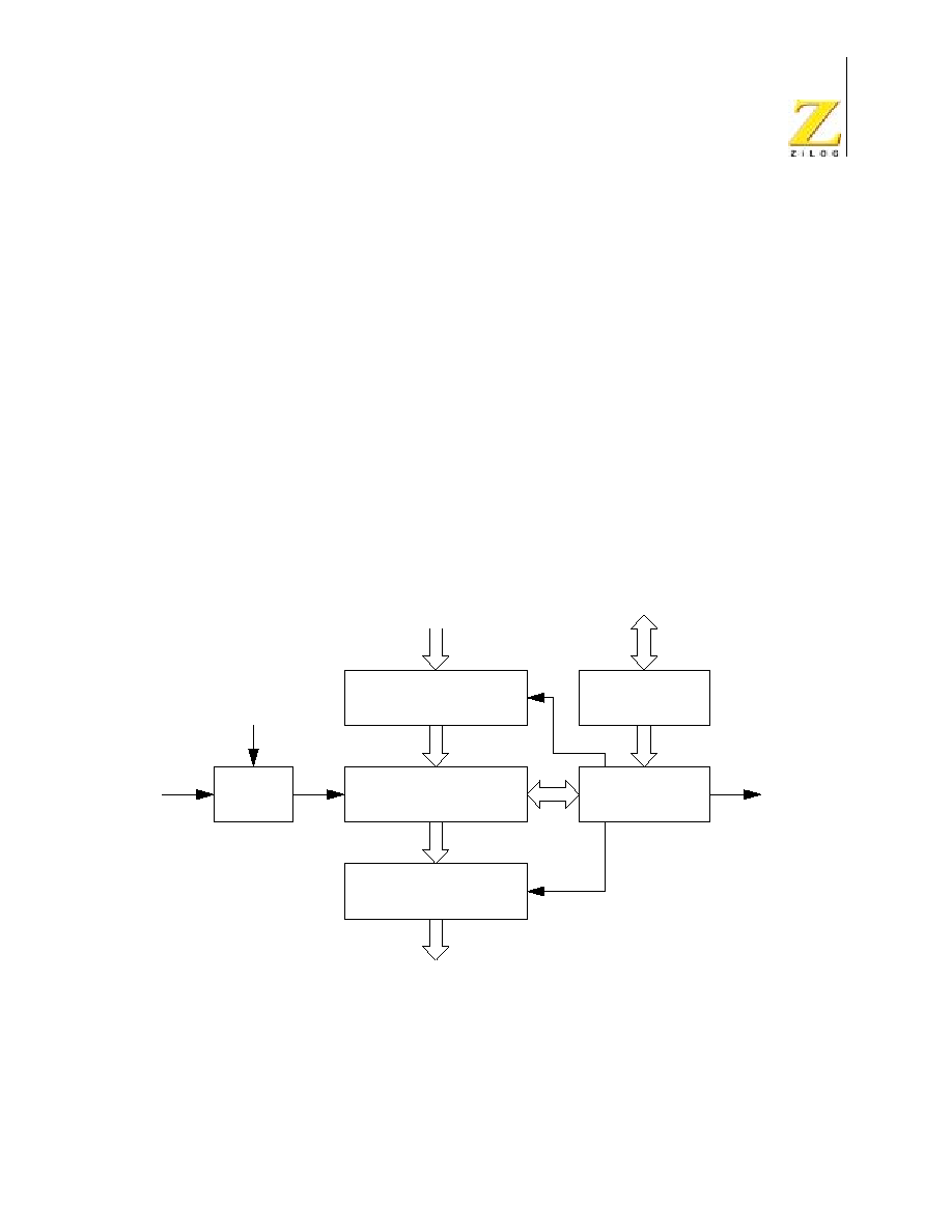
eZ80190 Product Specification
PS006611-0703
PRELIMINARY
Programmable Reload Timers
31
Programmable Reload Timers
Programmable Reload Timers Overview
The eZ80190 device features six Programmable Reload Timers (PRT). Each PRT
contains a 16-bit downcounter and a 16-bit reload register. In addition, each PRT
features a 4-bit clock prescaler with four selectable taps for CLK ˜ 2, CLK ˜ 4,
CLK ˜ 8 and CLK ˜ 16. Each timer can be individually enabled to operate in either
SINGLE PASS or CONTINUOUS mode. The timer can be programmed to start,
stop, restart from the current value, or restart from the initial value, and generate
interrupts for the CPU.
Each of the 6 PRTs available on the eZ80190 device can be controlled individu-
ally. They do not share the same counters, reload registers, control registers, or
interrupt signals. A simplified block diagram of a programmable reload timer is
shown in Figure 3.
Figure 3. Programmable Reload Timer Block Diagram
16-bit
Downcounter
Data Registers
{TMRx_DR_H,TMRx_DR_L}
Data[7:0]
Reload Registers
{TMRx_RR_H,TMRx_RR_L}
Clock
Adustable
Clock
Divider
Data[7:0]
Control Register
TMRx_CTL
Data[7:0]
TMRx_CTL[3:2]
PRT
Control Logic
Interrupt to
eZ80
Æ
CPU
eZ80190 Product Specification
PS006611-0703
PRELIMINARY
Programmable Reload Timers
32
Programmable Reload Timer Operation
Setting Timer Duration
There are three factors to consider when determining Programmable Reload
Timer duration--clock frequency, clock divider ratio, and initial count value. Mini-
mum duration of the timer is achieved by loading
0001h
,
because the timer times
out on the next clock edge. Maximum duration is achieved by loading
0000h
,
because the timer rolls over to
FFFFh
on the next clock edge and then continues
counting down to
0000h
.
The time-out period of the PRT is returned by the following equation:
SINGLE PASS Mode
In SINGLE PASS mode, when the end-of-count value,
0000h
, is reached, count-
ing halts, the timer is disabled, and the PRT_EN bit resets to 0. To restart the
timer, the CPU must reenable the timer by setting the PRT_EN bit to 1. An exam-
ple of a PRT operating in SINGLE PASS mode is illustrated in Figure 4. Timer reg-
ister information is indicated in Table 3.
PRT Time-Out Period =
Clock Divider Ratio x Reload Value
System Clock Frequency
Figure 4. PRT SINGLE PASS Mode Operation Example
CLK
IOWRN
Interrupt
Request
I/O Write to TMRx_CTL
Enables PRT
PRT Clock
(CLK/2)
PRT Count
Value
4
3
2
1
0
x
eZ80190 Product Specification
PS006611-0703
PRELIMINARY
Programmable Reload Timers
33
CONTINUOUS Mode
In CONTINUOUS mode, when the end-of-count value,
0000h
, is reached, the
timer automatically reloads the 16-bit start value from the Timer Reload registers,
TMRx_RR_H and TMRx_RR_L. Downcounting continues on the next clock edge.
In CONTINUOUS mode, the PRT continues to count until disabled. An example of
a PRT operating in CONTINUOUS mode is illustrated in Figure 5. Timer register
information is indicated in Table 4.
Table 3. PRT Single-Pass Mode Operation Example
Parameter
Control Register(s)
Value
PRT Enabled
TMRx_CTL[0]
1
Reload and Restart Enabled
TMRx_CTL[1]
1
PRT Clock Divider = 2
TMRx_CTL[3:2]
00b
Single-Pass Mode
TMRx_CTL[4]
0
PRT Interrupt Enabled
TMRx_CTL[6]
0
PRT Reload Value
{TMRx_RR_H, TMRx_RR_L}
0004h
Figure 5. PRT Continuous Mode Operation Example
CLK
IOWRN
Interrupt
Request
I/O Write to TMRx_CTL
Enables PRT
PRT Clock
(CLK/2)
PRT Count
Value
4
3
2
1
4
3
x

eZ80190 Product Specification
PS006611-0703
PRELIMINARY
Programmable Reload Timers
34
Reading the Current Count Value
The eZ80
Æ
CPU is capable of reading the current count value while the timer is
running. This READ event does not affect timer operation.
Timer Interrupts
The timer interrupt flag, PRT_IRQ, is set to 1 whenever the timer reaches its end-
of-count value,
0000h
, in SINGLE PASS mode, or when the timer reloads the start
value in CONTINUOUS mode. The timer interrupt flag is only set when the timer
reaches
0000h
(or reloads) from
0001h
. The timer interrupt flag is not set to 1
when the timer is loaded with the value
0000h
, which selects the maximum time-
out period.
The CPU can be programmed to poll the PRT_IRQ bit for the time-out event.
Alternatively, an interrupt service request signal can be sent to the CPU by setting
the IRQ_EN bit to 1. Then, when the end-of-count value,
0000h
, is reached and
the PRT_IRQ bit is set to 1, an interrupt service request signal is passed to the
CPU. The PRT_IRQ bit is cleared to 0 and the interrupt service request signal is
inactivated whenever the CPU reads from the timer control register, TMRx_CTL.
The response of the CPU to this interrupt service request is a function of the
CPU's interrupt enable flag, IEF1. For more information, refer to the
eZ80 CPU
User Manual
.
Programmable Reload Timer Registers
Each programmable reload timer is controlled using five 8-bit registers. These
registers are the TIMERx Control register, TIMERx Reload Low Byte register, TIM-
ERx Reload High Byte register, TIMERx Data Low Byte register, and TIMERx
Data High Byte register. The variable x can be 0, 1, 2, 3, 4, or 5, representing
each of the 6 available timers.
Table 4. PRT Continuous Mode Operation Example
Parameter
Control Register(s)
Value
PRT Enabled
TMRx_CTL[0]
1
Reload and Restart Enabled
TMRx_CTL[1]
1
PRT Clock Divider = 2
TMRx_CTL[3:2]
00b
Continuous Mode
TMRx_CTL[4]
1
PRT Interrupt Enabled
TMRx_CTL[6]
0
PRT Reload Value
{TMRx_RR_H, TMRx_RR_L}
0004h

eZ80190 Product Specification
PS006611-0703
PRELIMINARY
Programmable Reload Timers
35
The Timer Control register can be read or written to. The timer reload registers are
Write Only and are located at the same I/O address as the timer data registers,
which are Read Only.
Timer Control Registers
The Timer Control registers, detailed in Table 5, are used to control operation of
the timer, including enabling the timer, selecting the clock divider, enabling the
interrupt, selecting between CONTINUOUS and SINGLE PASS modes, and
enabling the automatic reload feature.
Table 5. Timer Control Register
(TMR0_CTL = 0080h, TMR1_CTL = 0083h, TMR2_CTL = 0086h,
TMR3_CTL = 0089h, TMR4_CTL = 008Ch, TMR5_CTL = 008Fh)
Bit
7
6
5
4
3
2
1
0
Reset
0
0
0
0
0
0
0
0
CPU Access
R
R/W
R/W
R/W
R/W
R/W
R/W
R/W
Note: R = Read Only; R/W = Read/Write.
Bit
Position
Value
Description
7
PRT_IRQ
0
The timer has not reached its end-of-count value. This bit is
reset to 0 every time the TMRx_CTL register is read.
1
The timer has reached its end-of-count value. If IRQ_EN is set
to 1, an interrupt signal is sent to the CPU. This bit remains 1
until the TMRx_CTL register is read.
6
IRQ_EN
0
Timer interrupt requests are disabled.
1
Timer interrupt requests are enabled.
5
0
Reserved
4
PRT_MODE
0
The timer operates in SINGLE PASS mode. PRT_EN (bit 0) is
reset to 0, and counting stops when the end-of-count value is
reached.
1
The timer operates in CONTINUOUS mode. The timer reload
value is written to the counter when the end-of-count value is
reached.
[3:2]
CLK_DIV
00
Clock ˜ 2 is the timer input source.
01
Clock ˜ 4 is the timer input source.
10
Clock ˜ 8 is the timer input source.
11
Clock ˜ 16 is the timer input source.

eZ80190 Product Specification
PS006611-0703
PRELIMINARY
Programmable Reload Timers
36
Timer Data Low Byte Register
This Read Only register returns the Low byte of the current count value of the
selected timer. The Timer Data Low Byte register, detailed in Table 6, can be read
while the timer is in operation. Reading the current count value does not affect
timer operation. To read the 16-bit data of the current count value,
{TMRx_DR_H[7:0], TMRx_DR_L[7:0]}, first read the Timer Data Low Byte register
and then read the Timer Data High Byte register. The Timer Data High Byte regis-
ter value is latched when a read of the Timer Data Low Byte register occurs.
The timer data registers and timer reload registers share the same
address space.
Timer Data High Byte Register
This Read Only register returns the High byte of the current count value of the
selected timer. The Timer Data High Byte register, detailed in Table 7, can be read
while the timer is in operation. Reading the current count value does not affect
timer operation. To read the 16-bit data of the current count value,
{TMRx_DR_H[7:0], TMRx_DR_L[7:0]}, first read the Timer Data Low Byte register
1
RST_EN
0
The automatic reload and restart function is disabled.
1
The automatic reload and restart function is enabled. When a 1
is written to RST_EN, the values in the reload registers are
loaded into the downcounter and the timer restarts.
0
PRT_EN
0
The programmable reload timer is disabled.
1
The programmable reload timer is enabled.
Table 6. Timer Data Low Byte Register
(TMR0_DR_L = 0081h, TMR0_DR_L = 0084h,
TMR0_DR_L = 0087h, TMR0_DR_L = 008Ah, TMR0_DR_L = 008Dh)
Bit
7
6
5
4
3
2
1
0
Reset
0
0
0
0
0
0
0
0
CPU Access
R
R
R
R
R
R
R
R
Note: R = Read Only.
Bit
Position
Value
Description
[7:0]
TMR_DR_L
00h≠FFh These bits represent the Low byte of the 2-byte timer data
value, {TMRx_DR_H[7:0], TMRx_DR_L[7:0]}. Bit 7 is bit 7
of the 16-bit timer data value. Bit 0 is bit 0 (lsb) of the 16-
bit timer data value.
Note:

eZ80190 Product Specification
PS006611-0703
PRELIMINARY
Programmable Reload Timers
37
and then read the Timer Data High Byte register. The Timer Data High Byte regis-
ter value is latched when a read of the Timer Data Low Byte register occurs.
The timer data registers and timer reload registers share the same
address space.
Timer Reload Low Byte Registers
The Timer Reload Low Byte registers, detailed in Table 8, stores the most signifi-
cant byte (MSB) of the 2-byte timer reload value. In CONTINUOUS mode, the
timer reload value is reloaded into the timer upon end-of-count. When the
RST_EN bit (TMRx_CTL[1]) is set to 1 to enable the automatic reload and restart
function, the timer reload value is written to the timer on the next rising edge of the
clock.
The timer data registers and timer reload registers share the same
address space.
Table 7. Timer Data High Byte Registers
(TMR0_DR_H = 0082h, TMR1_DR_H = 0085h,
TMR2_DR_H = 0088h, TMR3_DR_H = 008Bh, TMR4_DR_H = 008Eh)
Bit
7
6
5
4
3
2
1
0
Reset
0
0
0
0
0
0
0
0
CPU Access
R
R
R
R
R
R
R
R
Note: R = Read Only.
Bit
Position
Value
Description
[7:0]
TMR_DR_H
00h≠FFh These bits represent the High byte of the 2-byte timer
data value, {TMRx_DR_H[7:0], TMRx_DR_L[7:0]}. Bit 7 is
bit 15 (msb) of the 16-bit timer data value. Bit 0 is bit 8 of
the 16-bit timer data value.
Note:
Note:
eZ80190 Product Specification
PS006611-0703
PRELIMINARY
Programmable Reload Timers
38
Timer Reload High Byte Registers
The Timer Reload High Byte registers, detailed in Table 9, stores the most signifi-
cant byte (MSB) of the 2-byte timer reload value. In CONTINUOUS mode, the
timer reload value is reloaded into the timer upon reaching an end-of-count. When
the RST_EN bit (TMRx_CTL[1]) is set to 1 to enable the automatic reload and
restart function, the timer reload value is written to the timer on the next rising
edge of the clock.
The timer data registers and timer reload registers share the same
address space.
Table 8. Timer Reload Low Byte Registers
(TMR0_RR_L = 0081h, TMR1_RR_L = 0084h,
TMR2_RR_L = 0087h, TMR3_RR_L = 008Ah, TMR4_RR_L = 008Dh)
Bit
7
6
5
4
3
2
1
0
Reset
0
0
0
0
0
0
0
0
CPU Access
W
W
W
W
W
W
W
W
Note: W = Write Only.
Bit
Position
Value
Description
[7:0]
TMR_RR_L
00h≠FFh These bits represent the Low byte of the 2-byte timer
reload value, {TMRx_RR_H[7:0], TMRx_RR_L[7:0]}. Bit 7
is bit 7 of the 16-bit timer reload value. Bit 0 is bit 0 (lsb) of
the 16-bit timer reload value.
Table 9. Timer Reload High Byte Registers
(TMR0_RR_H = 0082h, TMR1_RR_H = 0085h,
TMR2_RR_H = 0088h, TMR3_RR_H = 008Bh, TMR4_RR_H = 008Eh)
Bit
7
6
5
4
3
2
1
0
Reset
0
0
0
0
0
0
0
0
CPU Access
W
W
W
W
W
W
W
W
Note: W = Write Only.
Bit
Position
Value
Description
[7:0]
TMR_RR_H
00h≠FFh These bits represent the High byte of the 2-byte timer
reload value, {TMRx_RR_H[7:0], TMRx_RR_L[7:0]}. Bit 7
is bit 15 (msb) of the 16-bit timer reload value. Bit 0 is bit 8
of the 16-bit timer reload value.
Note:
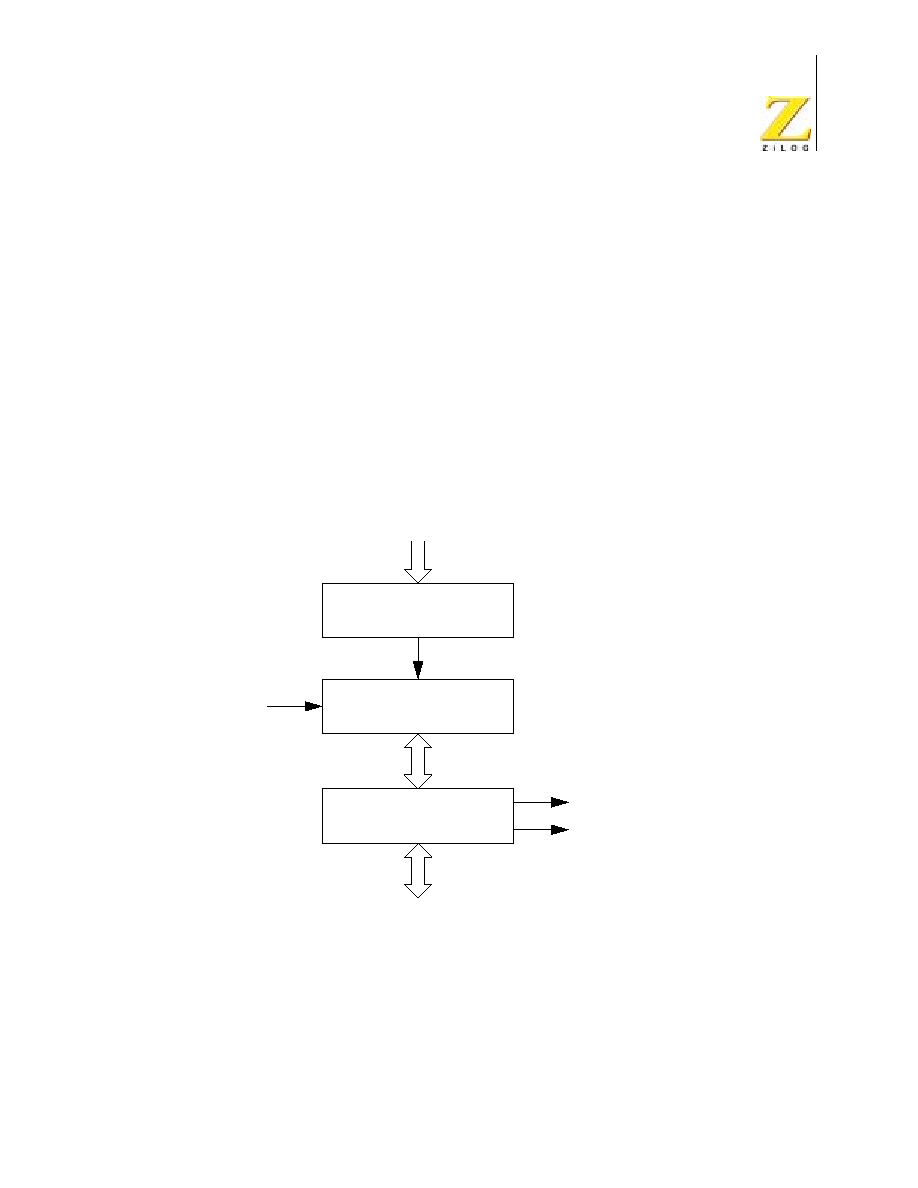
eZ80190 Product Specification
PS006611-0703
PRELIMINARY
Watch-Dog Timer
39
Watch-Dog Timer
Watch-Dog Timer Overview
The eZ80190 device includes a Watch-Dog Timer (WDT), which features:
∑
Four programmable time-out periods: 2
18
, 2
22
, 2
25
, and 2
27
clock cycles
∑
A WDT time-out RESET indicator flag
∑
A selectable time-out response: a time-out generates a RESET or a
nonmaskable interrupt
Figure 6 illustrates the block diagram for the Watch-Dog Timer.
Figure 6. Watch-Dog Timer Block Diagram
Watch-Dog Timer
Upcounter
WDT Control Register
and
Data[7:0]
WDT Reset Register
Clock
Data[7:0]
RESET
and
Reset Control Logic
Control Logic
NMI to eZ80
Æ
CPU

eZ80190 Product Specification
PS006611-0703
PRELIMINARY
Watch-Dog Timer
40
Watch-Dog Timer Operation
Enabling And Disabling The WDT
The Watch-Dog Timer is disabled upon a system RESET. To enable the WDT, the
application program must set the WDT_EN bit (bit 7) of the WDT_CTL register.
When enabled, the WDT cannot be disabled without a system RESET.
Time-Out Period Selection
There are four choices of time-out periods for the WDT--2
18
, 2
22
, 2
25
, and 2
27
system clock cycles. With a 50-MHz crystal oscillator, the available WDT time-out
periods are approximately 5.24
ms, 83.9
ms, 671
ms, and 2.68
s. The WDT time-
out period is defined by the WDT_PERIOD field of the WDT_CTL
register
(WDT_CTL[1:0]).
RESET Or NMI Generation
Upon a WDT time-out, the RST_FLAG bit in the WDT_CTL register is set to 1. In
addition, the WDT can cause a system RESET or send a nonmaskable interrupt
(NMI) signal to the CPU. The default operation is for the WDT to cause a system
RESET. The reset pulse generated by a Watch-Dog Timer time-out is 64
clock
cycles wide. It asserts/deasserts on the rising edge of the clock. The RST_FLAG
bit can be polled by the CPU to determine the source of the RESET event.
If the NMI_OUT bit in the WDT_CTL register is set to 1, then upon time-out, the
WDT asserts an NMI for CPU processing. The RST_FLAG bit can be polled by
the CPU to determine the source of the NMI event.
Watch-Dog Timer Registers
Watch-Dog Timer Control Register
The Watch-Dog Timer Control register, detailed in Table 10, is an 8-bit Read/Write
register used to enable the Watch-Dog Timer, set the time-out period, indicate the
source of the most recent RESET, and select the required operation upon WDT
time-out.

eZ80190 Product Specification
PS006611-0703
PRELIMINARY
Watch-Dog Timer
41
Table 10. Watch-Dog Timer Control Register
(WDT_CTL = 93h)
Bit
7
6
5
4
3
2
1
0
Reset
0
0
0/1
0
0
0
0
0
CPU Access
R/W
R/W
R
R
R
R
R/W
R/W
Note: R = Read Only; R/W = Read/Write.
Bit
Position
Value
Description
7
WDT_EN
0
WDT is disabled.
1
WDT is enabled. When enabled, the WDT cannot be disabled
without a full-chip reset.
6
NMI_OUT
0
WDT time-out resets the CPU.
1
WDT time-out generates a nonmaskable interrupt (NMI) to the
CPU.
5
RST_FLAG
0
RESET caused by external full-chip reset or ZDI reset.
1
RESET caused by WDT time-out. This flag is set by the WDT
time-out, even if the NMI_OUT flag is set to 1. The CPU can
poll this bit to determine the source of the RESET or NMI.
[4:2]
000
Reserved.
[1:0]
WDT_PERIOD
00
WDT time-out period is 134,217,728 (2
27
)
clock cycles.
01
WDT time-out period is 33,554,432 (2
25
)
clock cycles.
10
WDT time-out period is 4,194,304 (2
22
)
clock cycles.
11
WDT time-out period is 262,144 (2
18
)
clock cycles.

eZ80190 Product Specification
PS006611-0703
PRELIMINARY
Watch-Dog Timer
42
Watch-Dog Timer Reset Register
The Watch-Dog Timer Reset register, detailed in Table 11, is an 8-bit Write Only
register. The Watch-Dog Timer is reset when an
A5h
value followed by
5Ah
is writ-
ten to this register. Any amount of time can occur between the writing of the
A5h
value and the
5Ah
value, so long as the WDT time-out does not occur prior to
completion.
Table 11. Watch-Dog Timer Reset Register
(WDT_RR = 94h)
Bit
7
6
5
4
3
2
1
0
Reset
X
X
X
X
X
X
X
X
CPU Access
W
W
W
W
W
W
W
W
Note: X = Undefined; W = Write Only.
Bit
Position
Value
Description
[7:0]
WDT_RR
A5h
The first write value required to reset the WDT prior to a time-
out.
5Ah
The second write value required to reset the WDT prior to a
time-out. If an A5h, 5Ah sequence is written to WDT_RR, the
WDT timer is reset to its initial count value, and counting
resumes.

eZ80190 Product Specification
PS006611-0703
PRELIMINARY
General-Purpose Input/Output
43
General-Purpose Input/Output
GPIO Overview
The eZ80190 device features 32 General-Purpose Input/Output (GPIO) pins. The
GPIO pins are assembled as four 8-bit ports--Port A, Port B, Port C, and Port D.
All port signals can be configured for use as either inputs or outputs. In addition,
all of the port pins can be used as vectored interrupt sources for the eZ80
Æ
CPU.
GPIO Operation
GPIO operation is the same for all 4 GPIO ports (Ports A, B, C, and D). Each port
features eight GPIO port pins. The operating mode for each pin is controlled by
four bits that are divided between four 8-bit registers. These GPIO mode control
registers are:
∑
Port x Data Register (Px_DR)
∑
Port x Data Direction Register (Px_DDR)
∑
Port x Alternate Register 1 (Px_ALT1)
∑
Port x Alternate Register 2 (Px_ALT2)
where x can be A, B, C, or D, representing any of the four GPIO ports A, B, C, or
D. The mode for each pin is controlled by setting each register bit pertinent to the
pin to be configured. For example, the operating mode for Port B Pin 7 (PB7) is
set by the values contained in PB_DR[7], PB_DDR[7], PB_ALT1[7], and
PB_ALT2[7].
The combination of the GPIO control register bits allows individual configuration of
each port pin for nine modes. In all modes, reading the Port x Data register
returns the sampled state, or level, of the signal on the corresponding pin.
Table 12 indicates the function of each port signal based upon these four register
bits. After a RESET event, all GPIO port pins are configured as standard digital
inputs, with interrupts disabled.

eZ80190 Product Specification
PS006611-0703
PRELIMINARY
General-Purpose Input/Output
44
GPIO Mode 1. The port pin is configured as a standard digital output pin. The
value written to the Port x Data register (Px_DR) is presented on the pin.
GPIO Mode 2. The port pin is configured as a standard digital input pin. The out-
put is tristated (high impedance). The value stored in the Port x Data register pro-
duces no effect. As in all modes, a read from the Port x Data register returns the
pin's value. GPIO Mode 2 is the default operating mode following a RESET.
GPIO Mode 3. The port pin is configured as open-drain I/O. The GPIO pins do not
feature an internal pull-up to the supply voltage. To employ the GPIO pin in open-
drain mode, an external pull-up resistor must connect the pin to the supply volt-
age. Writing a 0 to the Port x Data register outputs a Low at the pin. Writing a 1 to
the Port x Data register results in high-impedance output.
GPIO Mode 4. The port pin is configured as open-source I/O. The GPIO pins do
not feature an internal pull-down to the supply ground. To employ the GPIO pin in
Table 12. GPIO Mode Selection
GPIO
Mode
Px_ALT2
Bits7:0
Px_ALT1
Bits7:0
Px_DDR
Bits7:0
Px_DR
Bits7:0 Port Mode
Output
1
0
0
0
0
Output
0
0
0
0
1
Output
1
2
0
0
1
0
Input from pin
High impedance
0
0
1
1
Input from pin
High impedance
3
0
1
0
0
Open-Drain output
0
0
1
0
1
Open-Drain I/O
High impedance
4
0
1
1
0
Open source I/O
High impedance
0
1
1
1
Open source output
1
5
1
0
0
0
Reserved
High impedance
6
1
0
0
1
Interrupt--dual edge triggered
High impedance
7
1
0
1
0
Port A or B--input from pin, high-impedance output.
Port C or D--alternate function controls port I/O.
1
0
1
1
Port A or B--input from pin, high-impedance output.
Port C or D--alternate function controls port I/O.
8
1
1
0
0
Interrupt--active Low
High impedance
1
1
0
1
Interrupt--active High
High impedance
9
1
1
1
0
Interrupt--falling edge triggered
High impedance
1
1
1
1
Interrupt--rising edge triggered
High impedance

eZ80190 Product Specification
PS006611-0703
PRELIMINARY
General-Purpose Input/Output
45
open-source mode, an external pull-down resistor must connect the pin to the
supply ground. Writing a 1 to the Port x Data register outputs a High at the pin.
Writing a 0 to the Port x Data register results in a high-impedance output.
GPIO Mode 5. Reserved. This pin produces high-impedance output.
GPIO Mode 6. The bit enables a dual-edge-triggered interrupt mode. Both a ris-
ing and a falling edge on the pin cause an interrupt request to be sent to the CPU.
Writing a 1 to the Port x Data register bit position resets the corresponding inter-
rupt request. Writing a 0 produces no effect. The programmer must set the Port x
Data register before entering the dual-edge-triggered interrupt mode.
GPIO Mode 7. For Ports C and D, the port pin is configured to pass control over
to the alternate functions assigned to the pin. For example, the alternate mode
function for PC7 is RI1. When GPIO Mode 7 is enabled, the pin output data and
pin tristate control come from the alternate function's data output and tristate con-
trol, respectively. The value in the Port x Data register produces no effect on oper-
ation.
For Ports A and B, which do not feature alternate I/O functions, selecting GPIO
Mode 7 results in a configuration of the pins for input from the pin and high-imped-
ance output as in GPIO Mode 2.
GPIO Mode 8. The port pin is configured for level-sensitive interrupt modes. An
interrupt request is generated when the level at the pin is the same as the level
stored in the Port x Data register. The port pin value is sampled by the system
clock. The input pin must be held at the selected interrupt level for a minimum of 2
clock periods to initiate an interrupt. The interrupt request remains active as long
as this condition is maintained at the external source.
GPIO Mode 9. The port pin is configured for single-edge-triggered interrupt
mode. The value in the Port x Data register determines if a positive or negative
edge causes an interrupt request. A 0 in the Port x Data register bit sets the
selected pin to generate an interrupt request for falling edges. A 1 in the Port x
Data register bit sets the selected pin to generate an interrupt request for rising
edges. The interrupt request remains active until a 1 is written to the Port x Data
register bit's corresponding interrupt request. Writing a 0 produces no effect on
operation. The programmer must set the Port x Data register before entering the
single-edge-triggered interrupt mode.
A simplified block diagram of a GPIO port pin is illustrated in Figure 7.
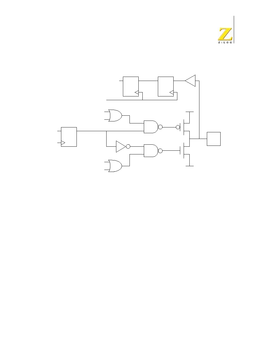
eZ80190 Product Specification
PS006611-0703
PRELIMINARY
General-Purpose Input/Output
46
GPIO Interrupts
Each port pin can be used as an interrupt source. Interrupts can be either level- or
edge-triggered.
Level-Triggered Interrupts
When the port is configured for level-triggered interrupts, the corresponding port
pin is tristated. An interrupt request is generated when the level at the pin is the
same as the level stored in the Port x Data register. The port pin value is sampled
by the system clock. The input pin must be held at the selected interrupt level for a
minimum of 2 clock periods to initiate an interrupt. The interrupt request remains
active as long as this condition is maintained at the external source.
For example, if PA3 is programmed for low-level interrupt and the pin is forced
Low for 2 clock cycles, an interrupt request signal is generated from that port pin
and sent to the CPU. The interrupt request signal remains active until the external
device driving PA3 forces the pin High. The CPU must be enabled to respond to
interrupts for the interrupt request signal to be acted upon.
Figure 7. GPIO Port Pin Block Diagram
D
Q
D
Q
D
Q
GND
VDD
Mode 1
Mode 4
Mode 1
Mode 3
GPIO Data
Register (Output)
GPIO Data
Register (Input)
Port
Pin
DATA
Bus
System
Clock
System
Clock

eZ80190 Product Specification
PS006611-0703
PRELIMINARY
General-Purpose Input/Output
47
Edge-Triggered Interrupts
When the port is configured for edge-triggered interrupts, the corresponding port
pin is tristated. If the pin receives the correct edge from an external device, the
port pin generates an interrupt request signal to the CPU. Any time a port pin is
configured for edge-triggered interrupt, writing a 1 to that pin's Port x Data register
causes a reset of the edge-triggered interrupt. The programmer must set the bit in
the Port x Data register to 1 before entering either single- or dual-edge-triggered
interrupt mode for that port pin.
When configured for dual-edge-triggered interrupt mode (GPIO Mode 6), both a
rising and a falling edge on the pin cause an interrupt request to be sent to the
CPU.
When configured for single-edge-triggered interrupt mode (GPIO Mode 9), the
value in the Port x Data register determines if a positive or negative edge causes
an interrupt request. A 0 in the Port x Data register bit sets the selected pin to gen-
erate an interrupt request for falling edges. A 1 in the Port x Data register bit sets
the selected pin to generate in interrupt request for rising edges.
GPIO Control Registers
The 16 GPIO Control Registers operate in groups of 4 with a set for each Port (A,
B, C, and D). Each GPIO port features a Port Data register, Port Data Direction
register, Port Alternate register 1, and Port Alternate register 2.
Port x Data Registers
When the port pins are configured for one of the output modes, the data written to
the Port x Data registers, detailed in Table 13, are driven on the corresponding
pins. In all modes, reading from the Port x Data registers always returns the cur-
rent sampled value of the corresponding pins. When the port pins are configured
as edge-triggered interrupt sources, writing a 1 to the corresponding bit in the Port
x Data register clears the interrupt signal that is sent to the CPU. When the port
pins are configured for edge-selectable interrupts or level-sensitive interrupts, the
value written to the Port x Data register bit selects the interrupt edge or interrupt
level. See
Table 12
on page 44 for more information.
Table 13. Port x Data Registers
(PA_DR = 96h, PB_DR = 9Ah, PC_DR = 9Eh, PD_DR = A2h)
Bit
7
6
5
4
3
2
1
0
Reset
X
X
X
X
X
X
X
X
CPU Access
R/W
R/W
R/W
R/W
R/W
R/W
R/W
R/W
Note: X = Undefined; R/W = Read/Write.
eZ80190 Product Specification
PS006611-0703
PRELIMINARY
General-Purpose Input/Output
48
Port x Data Direction Registers
In conjunction with the other GPIO Control Registers, the Port x Data Direction
registers, detailed in Table 14, control the operating modes of the GPIO port pins.
See
Table 12
on page 44 for more information.
Port x Alternate Registers 1
In conjunction with the other GPIO Control Registers, the Port x Alternate
Register 1, detailed in Table 15, control the operating modes of the GPIO port
pins. See
Table 12
on page 44 for more information.
Port x Alternate Registers 2
In conjunction with the other GPIO Control Registers, the Port x Alternate
Register 2, detailed in Table 16, control the operating modes of the GPIO port
pins. See
Table 12
on page 44 for more information.
Table 14. Port x Data Direction Registers
(PA_DDR = 97h, PB_DDR = 9Bh, PC_DDR = 9Fh, PD_DDR = A3h)
Bit
7
6
5
4
3
2
1
0
Reset
1
1
1
1
1
1
1
1
CPU Access
R/W
R/W
R/W
R/W
R/W
R/W
R/W
R/W
Note: R/W = Read/Write.
Table 15. Port x Alternate Registers 1
(PA_ALT1 = 98h, PB_ALT1 = 9Ch, PC_ALT1 = A0h, PD_ALT1 = A4h)
Bit
7
6
5
4
3
2
1
0
Reset
0
0
0
0
0
0
0
0
CPU Access
R/W
R/W
R/W
R/W
R/W
R/W
R/W
R/W
Note: R/W = Read/Write.
Table 16. Port x Alternate Registers 2
(PA_ALT2 = 99h, PB_ALT2 = 9Dh, PC_ALT2 = A1h, PD_ALT2 = A5h)
Bit
7
6
5
4
3
2
1
0
Reset
0
0
0
0
0
0
0
0
CPU Access
R/W
R/W
R/W
R/W
R/W
R/W
R/W
R/W
Note: R/W = Read/Write.

eZ80190 Product Specification
PS006611-0703
PRELIMINARY
Chip Selects and Wait States
49
Chip Selects and Wait States
The eZ80190 device generates four Chip Selects for external devices. Each Chip
Select may be programmed to access either memory space or I/O space. The
Memory Chip Selects can be individually programmed on a 64
KB boundary. The
I/O Chip Selects can each choose a 16-byte section of I/O space. In addition,
each Chip Select may be programmed for up to 7 WAIT states.
Memory and I/O Chip Selects
Each of the 4 available Chip Selects can be enabled for either the memory
address space or the I/O address space, but not both. To select the memory
address space for a particular Chip Select, CS_IO (CSx_CTL[4]) must be reset to
0. To select the I/O address space for a particular Chip Select, CS_IO must be set
to 1. After RESET, the default is for all Chip Selects to be configured for the mem-
ory address space. For either the memory address space or the I/O address
space, the individual Chip Selects must be enabled by setting CS_EN
(CSx_CTL[3]) to 1.
Memory Chip Select Operation
Each of the 4 Memory Chip Selects features 3 control registers. To enable a par-
ticular Memory Chip Select, the following conditions must be met:
∑
The Chip Select is enabled by setting CS_EN to 1
∑
The Chip Select is configured for memory by clearing CS_IO to 0
∑
The address is in the associated Chip Select range:
CSx_LBR[7:0]
ADDR[23:16] CSx_UBR[7:0]
∑
No higher priority (lower number) Chip Select meets the above 3 conditions
∑
No on-chip RAM is configured for the same address space, because on-chip
RAM is prioritized higher than all Memory Chip Selects
∑
A memory access instruction must be executing
If all of the foregoing conditions are met to generate a Memory Chip Select, then
the following actions occur:
∑
A Chip Select--CS0, CS1, CS2, or CS3--is activated (driven Low)
∑
The MREQ signal is activated (driven Low)

eZ80190 Product Specification
PS006611-0703
PRELIMINARY
Chip Selects and Wait States
50
∑
Depending upon the instruction, either RD or WR are activated (driven Low)
If the upper and lower bounds are set to the same value, such that CSx_UBR =
CSx_LBR, then a particular Chip Select is valid for, at most, a single 64
KB page.
Again, if a higher-priority Chip Select also encompasses the same set of
addresses, then the lower-priority Chip Select is not generated.
Memory Chip Select Priority
A lower-numbered Chip Select is granted priority over a higher-numbered Chip
Select. If the Chip Select 0 address space overlaps the Chip Select 1 address
space, Chip Select 0 is active. If the address range programmed for any Chip
Select signal overlaps with the address of internal RAM, then RAM is accorded
higher priority. If the particular Chip Select(s) feature an address range that over-
laps with the RAM address, then when RAM is selected, the Chip Select signal is
not asserted.
Reset States
On reset, Chip Select 0 is active for all addresses, because its Lower Bound reg-
ister resets to
0000h
and its Upper Bound register resets to
FFFFh
. All of the other
Chip Select Lower and Upper Bound registers reset to
0000h
.
Memory Chip Select Example
The use of Memory Chip Selects is demonstrated in Figure 8. The associated
control register values indicated in Table 17. In this example, all 4 Chip Selects
are enabled and configured for memory addresses. CS0, CS1, and CS2 are all
configured such that their address spaces do not overlap. CS3 is allocated an
address space that spans the entire 16
MB of available memory. Consequently,
CS3 overlaps the address spaces for CS0, CS1, and CS2. However, because
CS3 is the lowest-priority Chip Select, it only becomes active where it does not
overlap either CS0, CS1, or CS2.

eZ80190 Product Specification
PS006611-0703
PRELIMINARY
Chip Selects and Wait States
51
Figure 8. Memory Chip Select Example
Table 17. Register Values for Memory Chip Select Example
Chip
Select
CSx_CTL[3]
CSx_EN
CSx_CTL[4]
CSx_IO
CSx_LBR CSx_UBR Description
CS0
1
0
00h
7Fh
CS0 is enabled as a Memory Chip Select.
Valid addresses range from 000000h to
7FFFFFh.
CS1
1
0
80h
9Fh
CS1 is enabled as a Memory Chip Select.
Valid addresses range from 800000h to
9FFFFFh.
CS2
1
0
A0h
CFh
CS2 is enabled as a Memory Chip Select.
Valid addresses range from A00000h to
CFFFFFh.
CS3
1
0
D0h
FFh
CS3 is enabled as a Memory Chip Select.
Valid addresses range from D00000h to
FFFFFFh.
FFFFFFh
000000h
7FFFFFh
CS0_LBR = CS1_LBR = 00h
Memory
Location
9FFFFFh
CS1_LBR = 9Fh
CS2_UBR = CFh
CS2_LBR = A0h
CS0_UBR = 7Fh
CS3_UBR = FFh
D00000h
CFFFFFh
A00000h
800000h
CS0 Active
CS1 Active
CS2 Active
CS3 Active
8MB Address Space
2MB Adddress Space
3MB Address Space
3MB Address Space
CS3_LBR = D0h

eZ80190 Product Specification
PS006611-0703
PRELIMINARY
Chip Selects and Wait States
52
I/O Chip Select Operation
I/O Chip Selects can only be active when the CPU is performing I/O instructions.
Because the I/O space is separate from the memory space in the eZ80190
device, there can never be a conflict between I/O and memory addresses.
The I/O Chip Select logic decodes 8 bits from the address bus, ADDR[11:4].
Because the upper byte of the address bus, ADDR[23:16], is ignored, the I/O
devices can always be accessed from within any memory mode (ADL or Z80).
The MBASE offset value used for setting the Z80 MEMORY mode page is also
always ignored.
Four I/O Chip Selects are available with the eZ80190 device. To generate a partic-
ular I/O Chip Select, the following conditions must be met:
∑
The Chip Select is enabled by setting CS_EN to 1
∑
The Chip Select is configured for I/O by setting CS_IO to 1
∑
An I/O Chip Select address match occurs--ADDR[11:4] = CSx_LBR[7:0]
∑
No higher-priority (lower-number) Chip Select meets the above conditions
∑
The lower byte of the I/O address is not within the on-chip peripheral address
range of
80h
to
FFh
. On-chip peripheral registers assume priority for all
addresses where
80h
ADDR[7:0]
FFh
∑
An I/O instruction must be executing
If all of the foregoing conditions are met to generate an I/O Chip Select, then the
following actions occur:
∑
A Chip Select--CS0, CS1, CS2, or CS3--is activated (driven Low)
∑
The IORQ signal is activated (driven Low)
∑
Depending upon the instruction, either RD or WR are activated (driven Low)
I/O Chip Select Precaution
For all I/O operations, the upper byte of the address bus, ADDR[23:16], is forced
to
00h
. The I/O Chip Selects do not compare the values stored in the CSx_LBR
registers to what is generally considered to be the High byte of the I/O address, or
ADDR[15:8]. Instead, the I/O Chip Selects compare the values stored in the
CSx_LBR registers to a byte taken from the middle of the I/O address, or
ADDR[11:4].
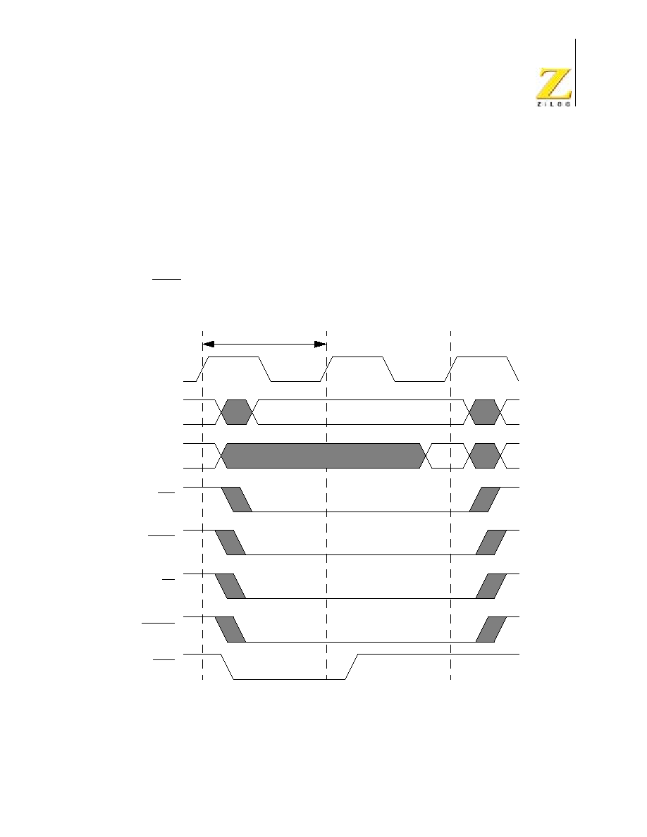
eZ80190 Product Specification
PS006611-0703
PRELIMINARY
Chip Selects and Wait States
53
Wait States
For each of the 4 available Chip Selects, programmable WAIT states can be
inserted to provide external devices with additional clock cycles to complete their
read and write operations. The number of WAIT states for a particular Chip Select
is controlled by the 3-bit field CSx_wait (CSx_CTL[7:5]). The Chip Selects can be
independently programmed to provide 0 to 7 WAIT states. The WAIT states idle
the CPU for the specified number of system clock cycles. An example of WAIT
state operation is illustrated in Figure 9. In this example, a single WAIT state is
added. It causes the instruction read operation to use an additional clock cycle.
WAIT is an internal signal used by the eZ80190 device and is illustrated in
Figure 9 for informational purposes only.
Figure 9. Wait State Operation Example
X
OUT
ADDR[23:0]
DATA[7:0]
CSx
MREQ
INSTRD
T
CLK
WAIT
(input)
RD

eZ80190 Product Specification
PS006611-0703
PRELIMINARY
Chip Selects and Wait States
54
Chip Select Registers
Chip Select x Lower Bound Register
For Memory Chip Selects, the Chip Select x Lower Bound register, detailed in
Table 18, defines the lower bound of the address range for which the correspond-
ing Memory Chip Select, if enabled, can be active. For I/O Chip Selects, this reg-
ister defines the address to which ADDR[11:4] is compared to generate an I/O
Chip Select. All Chip Select lower bound registers reset to
00h
.
Table 18. Chip Select x Lower Bound Register
(CS0_LBR = A8h, CS1_LBR = ABh, CS2_LBR = AEh, CS3_LBR = B1h)
Bit
7
6
5
4
3
2
1
0
Reset
0
0
0
0
0
0
0
0
CPU Access
R/W
R/W
R/W
R/W
R/W
R/W
R/W
R/W
Note: R/W = Read/Write.
Bit
Position
Value
Description
[7:0]
CS_LBR
00h≠
FFh
For Memory Chip Selects (CS_IO = 0)
This bit specifies the lower bound of the Chip Select address
range. The upper byte of the address bus, ADDR[23:16], is
compared to the values contained in these registers for
determining if a Memory Chip Select signal should be generated.
For I/O Chip Selects (CS_IO = 1)
This bit specifies the Chip Select address value. ADDR[11:4] is
compared to the values contained in these registers for
determining if an I/O Chip Select signal should be generated.

eZ80190 Product Specification
PS006611-0703
PRELIMINARY
Chip Selects and Wait States
55
Chip Select x Upper Bound Register
For Memory Chip Selects, the Chip Select x Upper Bound register, detailed in
Table 19, defines the upper bound of the address range for which the correspond-
ing Chip Select (if enabled) can be active. For I/O Chip Selects, this register pro-
duces no effect. The reset state for the Chip Select 0 Upper Bound register is
FFh
,
while the reset state for the 3 other Chip Select upper bound registers is
00h
.
Table 19. Chip Select x Upper Bound Register
(CS0_UBR = A9h, CS1_UBR = ACh, CS2_UBR = AFh, CS3_UBR = B2h)
Bit
7
6
5
4
3
2
1
0
CS0 Reset
1
1
1
1
1
1
1
1
CS1 Reset
0
0
0
0
0
0
0
0
CS2 Reset
0
0
0
0
0
0
0
0
CS3 Reset
0
0
0
0
0
0
0
0
CPU Access
R/W
R/W
R/W
R/W
R/W
R/W
R/W
R/W
Note: R/W = Read/Write.
Bit
Position
Value
Description
[7:0]
CS_UBR
00h≠
FFh
This bit specifies the upper bound of the Chip Select address
range. The upper byte of the address bus, ADDR[23:16], is
compared to the values contained in these registers for
determining if a Chip Select signal should be generated.

eZ80190 Product Specification
PS006611-0703
PRELIMINARY
Chip Selects and Wait States
56
Chip Select x Control Register
The Chip Select x Control register, detailed in Table 20, enables the Chip Selects,
specifies the type of Chip Select, and sets the number of WAIT states. The reset
state for the Chip Select 0 Control register is
E8h
, while the reset state for the 3
other Chip Select control registers is
00h
.
Table 20. Chip Select x Control Register
(CS0_CTL = AAh, CS1_CTL = ADh, CS2_CTL = B0h, CS3_CTL = B3h)
Bit
7
6
5
4
3
2
1
0
CS 0 Reset
1
1
1
0
1
0
0
0
CS 1 Reset
0
0
0
0
0
0
0
0
CS 2 Reset
0
0
0
0
0
0
0
0
CS 3 Reset
0
0
0
0
0
0
0
0
CPU Access
R/W
R/W
R/W
R/W
R/W
R/W
R/W
R/W
Note: R/W = Read/Write.
Bit
Position
Value
Description
[7:5]
CS_WAIT
000
0 WAIT states are inserted when this Chip Select is active.
001
1 WAIT state is inserted when this Chip Select is active.
010
2 WAIT states are inserted when this Chip Select is active.
011
3 WAIT states are inserted when this Chip Select is active.
100
4 WAIT states are inserted when this Chip Select is active.
101
5 WAIT states are inserted when this Chip Select is active.
110
6 WAIT states are inserted when this Chip Select is active.
111
7 WAIT states are inserted when this Chip Select is active.
4
CS_IO
0
An address match results in a Memory Chip Select.
1
An address match results in an I/O Chip Select.
3
CS_EN
0
Chip Select is disabled.
1
Chip Select is enabled.
[2:0]
000
Reserved--must be 000.

eZ80190 Product Specification
PS006611-0703
PRELIMINARY
Random Access Memory
57
Random Access Memory
The eZ80190 device features an 8
KB
x
8 single-port data Random Access Mem-
ory (RAM) for general-purpose use and a 1
KB
x
8 dual-port static RAM for use
with the Multiply-Accumulator unit. Both RAM spaces can be individually enabled
or disabled, and can be relocated to the top of any 64
KB page in memory. Data is
passed to and from the two RAM spaces via the 8-bit data bus, DATA[7:0]. The
dual-port MACC RAM can be used with the Multiply-Accumulator or as additional
general-purpose RAM, if required. For details about using the MACC RAM with
the Multiply-Accumulator, refer to
MACC RAM
on page 122.
The general-purpose data RAM occupies the memory addresses range
{RAM_ADDR_U[7:0],
E000h
} to {RAM_ADDR_U[7:0],
FFFFh
}. The Multiply-Accu-
mulator dual-port RAM occupies the address range {RAM_ADDR_U[7:0],
DC00h
}
to {RAM_ADDR_U[7:0],
DFFFh
}. An example of the memory mapping for the two
on-chip RAM spaces is illustrated in Figure 10. In this example, the RAM Address
Upper Byte register, RAM_ADDR_U, is set to
7Ah
. Figure 10 is not drawn to
scale, as RAM memories occupy only a very small fraction of the available 16
MB
address space.
When enabled, on-chip RAM assumes priority over all Memory Chip Selects that
may also be enabled in the same address space. If an address is generated in a
Figure 10. On-Chip RAM Memory Addressing Example
FFFFFFh
000000h
7ADC00h
7AE000h
7Ah
RAM_ADDR_U
Memory
Location
7ADFFFh
1KB MACC RAM
7AFFFFh
8KB
General-Purpose
RAM

eZ80190 Product Specification
PS006611-0703
PRELIMINARY
Random Access Memory
58
range that is covered by both the RAM address space and a particular Memory
Chip Select address space, the Memory Chip Select is not activated.
RAM Control Registers
RAM Control Register
The internal RAM spaces, data RAM and Multiply-Accumulator RAM, can be
enabled by setting corresponding bits in this register.
RAM Address Upper Byte Register
The RAM_ADDR_U register defines the upper byte of the address for the two on-
chip RAM blocks--general-purpose RAM and MACC RAM. If either or both of
these on-chip RAM blocks are enabled, their addresses assume priority over any
Chip Selects. The external Chip Select signals are not asserted if the correspond-
ing RAM address is enabled.
Table 21. RAM Control Register
(RAM_CTL
=
B4h)
Bit
7
6
5
4
3
2
1
0
Reset
0
0
0
0
0
0
0
0
CPU Access
R/W
R/W
R
R
R
R
R
R
Note: R/W = Read/Write.
Bit
Position
Value
Description
7
GPRAM_EN
0
On-chip general-purpose RAM is disabled.
1
On-chip general-purpose RAM is enabled.
6
MACRAM_EN
0
On-chip multiply-accumulator RAM is disabled.
1
On-chip multiply-accumulator RAM is enabled.
[5:0]
000000 Reserved

eZ80190 Product Specification
PS006611-0703
PRELIMINARY
Random Access Memory
59
Table 22. RAM Address Upper Byte Register
(RAM_ADDR_U
=
B5h)
Bit
7
6
5
4
3
2
1
0
Reset
0
0
0
0
0
0
0
0
CPU Access
R/W
R/W
R/W
R/W
R/W
R/W
R/W
R/W
Note: R/W = Read/Write.
Bit
Position
Value
Description
[7:0]
RAM_ADDR_U
00h≠
FFh
These bits define the upper byte of the RAM address. When
on-chip general-purpose RAM is enabled, the general-
purpose RAM address space ranges from {RAM_ADDR_U,
E000h} to {RAM_ADDR_U, FFFFh}. When on-chip MACC
RAM is enabled, the MACC RAM address space ranges from
{RAM_ADDR_U, DC00h} to {RAM_ADDR_U, DFFFh}. On-
chip RAM is prioritized higher than all other Memory Chip
Selects. If the enabled RAM and Chip Select addresses
overlap, the external Chip Select is not asserted.
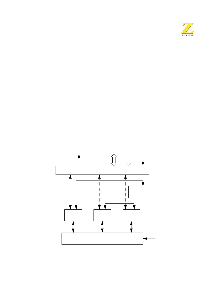
eZ80190 Product Specification
PS006611-0703
PRELIMINARY
Universal ZiLOG Interface
60
Universal ZiLOG Interface
The eZ80190 device features two on-chip Universal ZiLOG Interface (UZI)
devices. Each UZI contains three serial communication controller blocks: a Serial
Peripheral Interface (SPI), a Universal Asynchronous Receiver/Transmitter
(UART), and an Inter-Integrated Circuit serial bus (I
2
C). For each UZI device, any
one of these three communication controllers can be enabled. The UZI devices
are connected to General-Purpose I/O pins on Port C (UZI 1) and Port D (UZI 0).
Ports C and D must be configured for alternate-function I/O to allow the UZI
devices to communicate via the Port C and D pins. Each UZI also contains control
registers and a Baud Rate Generator (BRG) that generates a lower-frequency
clock for the SPI and UART devices. The I
2
C block features its own clock genera-
tor. The entire UZI block, including the Baud Rate Generator, is inactive when
none of the serial devices are selected. Figure 11 illustrates the UZI block dia-
gram.
Figure 11. UZI Block Diagram
UZI Interface
I/O
Address
Data
To eZ80
Æ
CPU
UZI
Interrupt
Clock
UART
SPI
I
2
C
GPIO Port C (UZI1) or Port D (UZIO)
Baud Rate
Generator
GPIO
Alternate
Function
Enable
Universal
ZiLOG
Interface

eZ80190 Product Specification
PS006611-0703
PRELIMINARY
Universal ZiLOG Interface
61
Please refer to the
Serial Peripheral Interface
,
Universal Asynchronous Receiver/
Transmitter
, and
I2C Serial I/O Interface
chapters for detailed operating informa-
tion. A description of the UZI Baud Rate Generator and the UZI control registers
appear in this chapter.
Baud Rate Generator
The Baud Rate Generator (BRG) is located within the UZI, but outside the three
serial communication controllers. The Baud Rate Generator creates a lower fre-
quency clock from the high-frequency system clock provided as an input to each
UZI. Baud Rate Generator output is used as the clock source by the SPI and the
UART. The I
2
C device generates its timing directly from the primary system clock.
Baud Rate Generator Functional Description
The Baud Rate Generator consists of a 16-bit downcounter, two registers, and
associated decoding logic. The Baud Rate Generator's initial value is defined by
the two BRG Divisor Latch registers, {BRGx_DLR_H, BRGx_DLR_L}. At the rising
edge of each system clock, the BRG decrements until it reaches the value
0001h
.
On the next system clock rising edge, the BRG reloads the initial value from
{BRGx_DLR_H, BRGx_DLR_L) and outputs a pulse to indicate the end-of-count.
Calculate the BRG output frequency with the following equation:
Upon RESET, the 16-bit BRG divisor value resets to the smallest allowable value
of
0002h
. Therefore, the minimum BRG clock divisor ratio is 2. A software write to
either the Low- or High-byte registers for the BRG Divisor Latch causes both the
Low and High bytes to load into the BRG counter, and causes the count to restart.
The divisor registers can only be accessed if bit 7 of the UART Line Control regis-
ter (UARTx_LCTL) is set to 1. After reset, this bit is reset to 0.
Recommended Usage of the Baud Rate Generator
The following is the normal sequence of operations that should occur after the
eZ80190 device is powered on to configure the UZI Baud Rate Generator:
∑
Assert and deassert RESET
∑
Set UARTx_LCTL[7] to 1 to enable access of the BRG divisor registers
∑
Program the BRGx_DLR_L and BRGx_DLR_H registers
∑
Clear UARTx_LCTL[7] to 0 to disable access of the BRG divisor registers.
BRGx Output Frequency =
System Clock Frequency
{BRGx_DLR_H, BRGx_DLR_L}

eZ80190 Product Specification
PS006611-0703
PRELIMINARY
Universal ZiLOG Interface
62
UZI and BRG Control Registers
UZI Control Registers
The UZI Control registers select between the three available serial communica-
tion controllers: I
2
C, SPI and UART. Each of the two UZI devices on the eZ80190
device features its own UZI Control register.
BRG Divisor Latch Registers--Low Byte
This register holds the Low byte of the 16-bit divisor count loaded by the proces-
sor for baud rate generation. The 16-bit clock divisor value is returned by
{BRGx_DLR_H, BRGx_DLR_L}, where x is either 0 or 1 to identify the two avail-
able UZI devices. Upon RESET, the 16-bit BRG divisor value resets to
0002h
. The
initial 16-bit divisor value must be between
0002h
and
FFFFh
as the values
0000h
and
0001h
are invalid and proper operation is not guaranteed. Thus the minimum
BRG clock divisor ratio is 2.
A write to either the Low or High byte registers for the BRG Divisor Latch causes
both bytes to be loaded into the BRG counter and the count restarted.
Bit 7 of the associated UART Line Control register (UARTx_LCTL) must be set to
1 to access this register for each UZI device. Refer to the
UART Line Control Reg-
ister
(UARTx_LCTL) on page 75 for more information.
The BRGx_DLR_L registers share the same address space with the UARTx_RBR
and UARTx_THR registers. Bit 7 of the associated UART Line Control register
(UARTx_LCTL) must be set to 1 to enable access for this register within each UZI
device.
Table 23. UZI Control Registers
(UZI0_CTL
=
CFh, UZI1_CTL
=
DFh)
Bit
7
6
5
4
3
2
1
0
Reset
0
0
0
0
0
0
0
0
CPU Access
R
R
R
R
R
R
R/W
R/W
Note: R = Read Only; R/W = Read/Write.
Bit
Position
Value
Description
[7:2]
000000 Reserved
[1:0]
UZI_MODE
00
All UZI devices are disabled.
01
UART is enabled.
10
SPI is enabled.
11
I
2
C is enabled.

eZ80190 Product Specification
PS006611-0703
PRELIMINARY
Universal ZiLOG Interface
63
BRG Divisor Latch Registers--High Byte
This register holds the High byte of the 16-bit divisor count loaded by the proces-
sor for baud rate generation. The 16-bit clock divisor value is returned by
{BRGx_DLR_H, BRGx_DLR_L} where x is either 0 or 1 to identify the two avail-
able UZI devices. Upon RESET, the 16-bit BRG divisor value resets to
0002h
. The
initial 16-bit divisor value must be between
0002h
and
FFFFh
because the values
0000h
and
0001h
are invalid, and proper operation is not guaranteed. Therefore,
the minimum BRG clock divisor ratio is 2.
A write to either the Low- or High-byte registers for the BRG Divisor Latch causes
both bytes to load into the BRG counter, and causes the count to restart.
Bit 7 of the associated UART Line Control register (UARTx_LCTL) must be set to
1 to access this register for each UZI device. Refer to the
UART Line Control Reg-
ister
(UARTx_LCTL) on page 75 for more information.
The BRGx_DLR_H registers share the same address space with the UARTx_IER
registers. Bit 7 of the associated UART Line Control register (UARTx_LCTL) must
be set to 1 to enable access for this register within each UZI device.
Table 24. BRG Divisor Latch Registers--Low Byte
BRG0_DLR_L = C0h, BRG1_DLR_L = D0h
Bit
7
6
5
4
3
2
1
0
Reset
0
0
0
0
0
0
0
0
CPU Access
R/W
R/W
R/W
R/W
R/W
R/W
R/W
R/W
Note: R = Read Only; R/W = Read/Write.
Bit
Position
Value
Description
[7:0]
BRG_DLR_L
00h≠
FFh
These bits represent the Low byte of the 16-bit Baud Rate
Generator divider value. The complete BRG divisor value is
returned by {BRG_DLR_H, BRG_DLR_L}.

eZ80190 Product Specification
PS006611-0703
PRELIMINARY
Universal ZiLOG Interface
64
Table 25. BRG Divisor Latch Registers--High Byte
(BRG0_DLR_H = C1h, BRG1_DLR_H = D1h)
Bit
7
6
5
4
3
2
1
0
Reset
0
0
0
0
0
0
0
0
CPU Access
R/W
R/W
R/W
R/W
R/W
R/W
R/W
R/W
Note: R = Read Only; R/W = Read/Write.
Bit
Position
Value
Description
[7:0]
BRG_DLR_H
00h≠
FFh
These bits represent the High byte of the 16-bit Baud Rate
Generator divider value. The complete BRG divisor value is
returned by {BRG_DLR_H, BRG_DLR_L}.
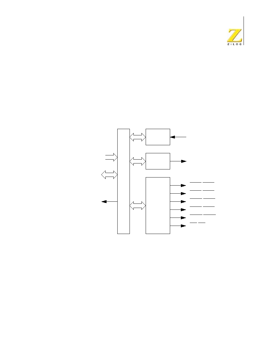
eZ80190 Product Specification
PS006611-0703
PRELIMINARY
Universal Asynchronous Receiver/Transmitter
65
Universal Asynchronous Receiver/
Transmitter
The UART module implements all of the logic required to support asynchronous
communications protocol. The module also implements two separate 16-byte
FIFOs for both transmit and receive. A block diagram of the UART is illustrated in
Figure 12.
The UART module provides the following asynchronous communications protocol
related features/functions.
∑
5, 6, 7 or 8-bit data transmission
∑
Even/odd or no parity bit generation and detection
∑
Start and stop bit generation and detection (supports up to two stop bits)
∑
Line break detection and generation
∑
Receiver overrun and framing error detection
∑
Logic and associated I/O to provide modem hand-shake capability
Figure 12. UART Block Diagram
Receive
Buffer
Transmit
Buffer
Modem
Control
Logic
UZI Interface
I/O
Address
Data
Interrupt
Signal
To eZ80
Æ
CPU
RxD0/RxD1
TxD0/TxD1
RTS0/RTS1
CTS0/CTS1
DSR0/DSR1
DTR0/DTR1
DCD0/DCD1
RI0/RI1

eZ80190 Product Specification
PS006611-0703
PRELIMINARY
Universal Asynchronous Receiver/Transmitter
66
UART Functional Description
The core uses an externally-provided clock from the Baud Rate Generator for the
serial transmit/receive function. The UART module supports all of the various
options in the asynchronous transmission and reception protocol including:
∑
5 to 8-bit transmit/receive
∑
Start bit generation and detection
∑
Parity generation and detection
∑
Stop bit generation and detection
∑
Break generation and detection
The UART contains 16-byte FIFOs in each direction. The FIFOs can be enabled
or disabled by the application. The receive FIFO features trigger-level detection
logic, which enables the processor to block transfer data bytes from the receive
FIFO.
The UART data transfer rate is calculated in the following equation:
UART Functions
The UART function implements:
∑
The transmitter and associated control logic
∑
The receiver and associated control logic
∑
The modem interface and associated logic
UART Transmitter
The transmitter block controls the data transmitted on the TXD output. It imple-
ments the FIFO, accessed through the UARTx_THR register, the transmit shift
register, the parity generator, and control logic for the transmitter to control param-
eters for the asynchronous communications protocol.
The UARTx_THR is a Write Only register. The processor writes the data byte to
be transmitted into this register. In FIFO mode, up to 16 data bytes can be written
through the UARTx_THR register. The data byte from the FIFO is transferred to
the transmit shift register and transmitted on the TXD pin. After SYNC_RESET,
the UARTx_THR register is empty so the Transmit Holding Register Empty
UART Data Transfer Rate (bits/s) =
System Clock Frequency
16 x Baud Rate Generator Divisor

eZ80190 Product Specification
PS006611-0703
PRELIMINARY
Universal Asynchronous Receiver/Transmitter
67
(THRE) bit (bit 5 of the UARTx_LSR register) is set to 1 and an interrupt is sent to
the processor (if interrupts are enabled). The processor can reset this interrupt by
loading data into the UARTx_THR register, which clears the transmitter interrupt.
The transmit shift register places the byte to be transmitted on the TXD signal
serially. The least significant bit of the byte to be transmitted is shifted out first and
the most significant bit is shifted out last. The control logic within the block adds
the asynchronous communications protocol bits to the data byte being transmit-
ted. The transmitter block obtains the parameters for the protocol from the bits
programmed through the UARTx_LCTL register. The TXD output is set to 1 if the
transmitter is idle (it does not contain any data to be transmitted).
The transmitter operates with the Baud Rate Generator (BRG) clock. The data
bits are placed on the TXD output one time every 16 BRG clock cycles. The trans-
mitter block also implements a parity generator and attaches the parity bit with the
byte if programmed to do so.
UART Receiver
The receiver block controls data reception from the RXD signal. The receiver
block implements a receiver shift register, receiver line error condition monitoring
logic and receiver data ready logic. It also implements a parity checker.
The processor reads received data from UARTx_RBR, which is a Read Only reg-
ister. The condition of the UARTx_RBR register is monitored by the DR bit (bit 0 of
the UARTx_LSR register). The DR bit is set to 1 when a data byte is received and
transferred to the UARTx_RBR register from the receiver shift register. The DR bit
is reset only when the processor reads all received data bytes. If the number of
bits received is less than eight, the unused most significant bits of the data byte
read are reset to 0.
The receiver uses the clock from the BRG input of the UZI for receiving data. This
clock must be 16 times the required baud rate. The receiver synchronizes the shift
clock on the falling edge of the RXD input start bit. It then receives a complete
byte according to the set parameters. The receiver also implements logic to detect
framing errors, parity errors, overrun errors, and break signals.
UART Modem Control
The modem control logic provides two outputs and four inputs for handshaking
with the modem. Any change in the modem status inputs, except RI, is detected.
An interrupt can then be generated. For RI, an interrupt is generated only when
the trailing edge of the RI is detected. The module also provides a loop mode for
self-diagnostic purposes.

eZ80190 Product Specification
PS006611-0703
PRELIMINARY
Universal Asynchronous Receiver/Transmitter
68
UART Interrupts
There are five different sources of interrupts from the UART. These five sources of
interrupts are:
∑
Transmitter
∑
Receiver (three different interrupts)
∑
Modem status
UART Transmitter Interrupt
The transmitter interrupt is generated if there is no data available for transmission.
This interrupt can be disabled using the individual interrupt enable bit, or cleared
by writing data into the UARTx_THR register.
UART Receiver Interrupts
A receiver interrupt can be generated by three possible events. The first event, a
receiver data ready interrupt event, indicates that one or more data bytes were
received and are ready to be read. If the FIFO is enabled, and the trigger level is
set, then this interrupt is generated if the number of bytes in the receive FIFO is
greater than or equal to the trigger level. If the FIFO is not enabled, the interrupt is
generated if the receive buffer contains a data byte. This interrupt is cleared by
reading the UARTx_RBR.
The second interrupt source is the receiver time-out. A receiver time-out interrupt
is generated when there are fewer data bytes in the receive FIFO than the trigger
level. There are no READs and writes to or from the receive FIFO for four consec-
utive byte times. After the receiver time-out interrupt is generated, it is cleared
only after it empties the entire receive FIFO.
The first two interrupt sources from the receiver (data ready and time-out) share
an interrupt enable bit.
The third source of a receiver interrupt is a line status error indicating an error in
byte reception. This error may result from:
∑
Incorrect received parity
∑
Incorrect framing (the stop bit is not detected by the receiver at the end of the
byte)
∑
Receiver overrun condition
∑
A Break Indication being detected on the receive data input
An interrupt due to one of the above conditions is cleared when the UARTx_LSR
register is read. In the case of FIFO mode, a line status interrupt is generated only

eZ80190 Product Specification
PS006611-0703
PRELIMINARY
Universal Asynchronous Receiver/Transmitter
69
after the received byte with an error reaches the top of the FIFO and is ready to be
read.
A line status interrupt is activated (provided this interrupt is enabled) as long as
the read pointer of the receive FIFO points to the location of the FIFO that con-
tains a byte with the error. The interrupt is immediately cleared when the
UARTx_LSR register is read. The ERR bit of the UARTx_LSR register is active as
long as an error byte is present in the receive FIFO.
UART Modem Status Interrupt
The modem status interrupt is generated if there is any change in state of the
modem status inputs to the UART. This interrupt is cleared when the processor
reads the UARTx_MSR register.
UART Recommended Usage
The following is the standard sequence of events that occurs in the eZ80190
device using the UART. A description of each follows.
∑
Module reset
∑
Control transfers to configure UART operation
∑
Data transfers
Module Reset
Upon reset, all internal registers return to their default values. All command status
registers are programmed with their default values and the FIFOs are flushed.
Control Transfers
Based on the application requirement, the data transfer baud rate is determined
and the BRG is configured to generate a 16X clock frequency, provided at the
BRG signal input. Interrupts are disabled and communication control parameters
are programmed in the UARTx_LCTL register. The FIFO configuration is deter-
mined and the receive trigger levels are set in the UARTx_FCTL register. The sta-
tus registers, UARTx_LSR and UARTx_MSR, are read to ensure that no interrupt
sources are active. Interrupts are enabled (except for the transmit interrupt) and
the application is ready to use the module for transmission and reception.
Data Transfers
Transmit. To transmit data, the application enables the transmit interrupt. An
interrupt is immediately expected in response to this interrupt. The application
reads the UARTx_IIR register and determines that the interrupt occurs because of
an empty UARTx_THR register. When the application determines this occurrence,

eZ80190 Product Specification
PS006611-0703
PRELIMINARY
Universal Asynchronous Receiver/Transmitter
70
the application writes the transmit data bytes to the UARTx_THR register. The
number of bytes that the application writes depends on whether or not the FIFO is
enabled. If the FIFO is enabled, the application can write 16 bytes at one time. If
the FIFO is not enabled, the application can Write Only one byte at a time. As a
result of the first write, the interrupt is deactivated. The processor then waits for
the next interrupt. When the interrupt is raised by the UART module, the proces-
sor repeats the same process until it exhausts all of the data for transmission.
To control and check the modem status, the application sets up the modem by
writing to UARTx_MCTL register and reading from the UARTx_MSR register
before starting the above process.
Receive. The receiver is always enabled and continually checks for the start bit
on the RXD input signal. When an interrupt is raised by the UART module, the
application reads the UARTx_IIR register and determines the cause of the inter-
rupt. If the cause is a line status interrupt, the application reads the UARTx_LSR
register, reads the data byte, then discards the byte or takes other action. If the
interrupt is caused by a RECEIVE DATA READY condition, the application alter-
nately reads the UARTx_LSR and UARTx_RBR registers and removes all
received data bytes. It reads the UARTx_LSR register before reading the
UARTx_RBR register to determine if there is a NO ERROR condition in the
received data.
To control and check modem status, the application sets up the modem by writing
to the UARTx_MCTL register and reading the UARTx_MSR register before start-
ing the above process.
Poll Mode Transfers
When interrupts are disabled, all data transfers are referred to as poll mode trans-
fers. In poll mode transfers, the application must continually poll the UARTx_LSR
register to transmit or receive data without enabling the interrupts. This condition
is also true for the UARTx_MSR register. If the interrupts are not enabled, the
data in the UARTx_IIR register cannot be used to determine the cause of an inter-
rupt.
UART Registers
After a system reset, all UART registers are set to their default values. Any writes
to unused registers or register bits are ignored. READs return a value of 0. For
compatibility with future versions of this part, unused bits within a register should
always be written with a value of 0. READ/WRITE attributes, reset conditions, and
bit descriptions of all UART registers are provided in this section.
eZ80190 Product Specification
PS006611-0703
PRELIMINARY
Universal Asynchronous Receiver/Transmitter
71
UART Transmit Holding Register
If less than eight bits are programmed for transmission, the lower bits of the byte
written to the UART Transmit Holding Register, indicated in Table 26, are selected
for transmission. The transmit FIFO is mapped at this address. The user can write
up to 16 bytes for transmission at one time to this address if the FIFO is enabled
by the application. If the FIFO is disabled, this buffer is only one byte deep. These
registers share the same address space as the UARTx_RBR and BRGx_DLR_L
registers.
UART Receive Buffer Register
The bits in this register reflect the data received. If less than eight bits are pro-
grammed for the receive function, the lower bits of the byte reflect the bits
received, whereas upper unused bits are 0. The receive FIFO is mapped at this
address. If the FIFO is disabled, this buffer is only one byte deep.
The registers in the UART Receive Buffer, indicated in Table 27, share the same
address space as the UARTx_THR and BRGx_DLR_L registers.
Table 26. UART Transmit Holding Registers
(UART0_THR = C0h, UART1_THR = D0h)
Bit
7
6
5
4
3
2
1
0
Reset
X
X
X
X
X
X
X
X
CPU Access
W
W
W
W
W
W
W
W
Note: W = Write Only.
Bit
Position
Value
Description
[7:0]
TXD
00h≠
FFh
Transmit data byte.
Table 27. UART Receive Buffer Registers
(UART0_RBR = C0h, UART1_RBR = D0h)
Bit
7
6
5
4
3
2
1
0
Reset
0
0
0
0
0
0
0
0
CPU Access
R
R
R
R
R
R
R
R
Note: R = Read Only.
Bit
Position
Value
Description
[7:0]
RXD
00h≠
FFh
Receive data byte.

eZ80190 Product Specification
PS006611-0703
PRELIMINARY
Universal Asynchronous Receiver/Transmitter
72
UART Interrupt Enable Register
The UARTx_IER register, indicated in Table 28, is used to enable and disable
UART interrupts. The UARTx_IER registers share the same I/O addresses as the
BRGx_DLR_H registers.
Table 28. UART Interrupt Enable Registers
(UART0_IER = C1h, UART1_IER = D1h)
Bit
7
6
5
4
3
2
1
0
Reset
0
0
0
0
0
0
0
0
CPU Access
R/W
R/W
R/W
R/W
R/W
R/W
R/W
R/W
Note: R/W = Read/Write.
Bit
Position
Value
Description
[7:4]
0000
Reserved
3
MIIE
0
The modem interrupt on edge detect of status inputs is
disabled.
1
The modem interrupt on edge detect of status inputs is
enabled.
2
LSIE
0
The line status interrupt is disabled.
1
The line status interrupt is enabled for receive data errors:
incorrect parity bit received, framing error, overrun error, or
break detection.
1
TIE
0
The transmit interrupt is disabled.
1
The transmit interrupt is enabled. An interrupt is generated
when the transmit FIFO buffer is empty indicating no bytes
are available for transmission.
0
RIE
0
The receive interrupt is disabled.
1
The receive interrupt and receiver time-out interrupt are
enabled. An interrupt is generated if the FIFO buffer contains
data ready for a READ or if the receiver times out.

eZ80190 Product Specification
PS006611-0703
PRELIMINARY
Universal Asynchronous Receiver/Transmitter
73
UART Interrupt Identification Register
The Read Only UART Interrupt Identification register, indicated in Table 29, allows
the user to check the status of interrupts and whether the FIFO is enabled. These
registers share the same I/O addresses as the UARTx_FCTL registers. Status
codes for the UARTx_IIR register are provided in Table 30.
Table 29. UART Interrupt Identification Registers
(UART0_IIR = C2h, UART1_IIR = D2h)
Bit
7
6
5
4
3
2
1
0
Reset
0
0
0
0
0
0
0
1
CPU Access
R
R
R
R
R
R
R
R
Note: R = Read Only.
Bit
Position
Value
Description
[7:6]
FSTS
00
FIFO is disabled.
11
FIFO is enabled.
[5:4]
00
Reserved
[3:1]
INSTS
000≠
110
Interrupt Status Code
The code indicated in these three bits is valid only if the
interrupt bit is 1. If two internal interrupt sources are active
and their respective enable bits are High, only the higher
priority interrupt is seen by the application. The lower priority
interrupt code is indicated only after the higher priority
interrupt is serviced.
Table 30
lists interrupt status codes.
0
INTBIT
0
There is an active interrupt source within the UART.
1
There is not an active interrupt source within the UART.
Table 30. UART Interrupt Status Codes
INSTS
Value
Priority
Interrupt Type
011
Highest
Receiver Line Status
010
Second
Receive Data Ready or Trigger Level
110
Third
Character Time-out
001
Fourth
Transmit Buffer Empty
000
Lowest
Modem Status

eZ80190 Product Specification
PS006611-0703
PRELIMINARY
Universal Asynchronous Receiver/Transmitter
74
UART FIFO Control Registers
These registers, indicated in Table 31, are used to monitor trigger levels, clear
FIFO pointers, and enable or disable the FIFO. The UARTx_FCTL registers share
the same I/O addresses as the UARTx_IIR registers.
Table 31. UART FIFO Control Registers
(UART0_FCTL = C2h, UART1_FCTL = D2h)
Bit
7
6
5
4
3
2
1
0
Reset
0
0
0
0
0
0
0
1
CPU Access
W
W
W
W
W
W
W
W
Note: W = Write Only.
Bit
Position
Value
Description
[7:6]
TRIG
00
The receive FIFO trigger level is set to 1. A receive data
interrupt is generated when there is 1 byte in the FIFO. This
bit is valid only if the FIFO is enabled.
01
The receive FIFO trigger level set to 4. The receive data
interrupt is generated when there are 4 bytes in the FIFO.
This bit is valid only if the FIFO is enabled.
10
The receive FIFO trigger level set to 8. The receive data
interrupt is generated when there are 8 bytes in the FIFO.
This bit is valid only if the FIFO is enabled.
11
The receive FIFO trigger level set to 14. The receive data
interrupt is generated when there are 14 bytes in the FIFO.
This bit is valid only if the FIFO is enabled.
[5:3]
000b
Reserved--must be 000b.
1
CLRTXF
0
This bit produces no effect.
1
This bit clears the transmit FIFO and resets the transmit FIFO
pointer. This bit is valid only if the FIFO is enabled.
2
CLRRXF
0
This bit produces no effect.
1
This bit clears the receive FIFO, clears the receive error FIFO,
and resets the receive FIFO pointer. This bit is valid only if the
FIFO is enabled.
0
FIFOEN
0
The transmit and receive FIFOs are disabled. The transmit
and receive buffers are only one byte deep.
1
The transmit and receive FIFOs are enabled.

eZ80190 Product Specification
PS006611-0703
PRELIMINARY
Universal Asynchronous Receiver/Transmitter
75
UART Line Control Register
These registers, indicated in Table 32, are used to control the communication con-
trol parameters. Table 33 defines character length and stop bit parameters.
Table 32. UART Line Control Registers
(UART0_LCTL = C3h, UART1_LCTL = D3h)
Bit
7
6
5
4
3
2
1
0
Reset
0
0
0
0
0
0
0
0
CPU Access
R/W
R/W
R/W
R/W
R/W
R/W
R/W
R/W
Note: R/W = Read/Write.
Bit
Position
Value
Description
7
DLAB
0
Access to the UART registers at I/O addresses C0h, C1h,
D0h and D1h is enabled.
1
Access to the Baud Rate Generator registers at I/O addresses
C0h, C1h, D0h and D1h is enabled.
6
SB
0
Do not send a break signal.
1
Send Break
UART sends a continuous 0 on the transmit output from the
next following bit boundary. The transmit data in the transmit
shift register is ignored. After assigning this bit High, the TXD
output is made 0 only after the bit boundary is reached. Just
before assigning a 0 to TXD, it clears the transmit FIFO one
time. Any new data written to the transmit FIFO during a break
should be written only after the THRE bit of the UARTx_LSR
register goes High. This new data is transmitted after the
UART recovers from the break. After the break is removed,
the UART recovers from break for the next BRG edge.
5
FPE
0
Do not force a parity error.
1
Force a parity error. When this bit and the party enable bit
(PEN) are both 1, an incorrect parity bit is transmitted with the
data byte.
4
EPS
0
Use odd parity for transmission. The total number of 1 bit in
the transmit data plus parity bit is odd.
1
Use even parity for transmission. The total number of 1 bit in
the transmit data plus parity bit is even.

eZ80190 Product Specification
PS006611-0703
PRELIMINARY
Universal Asynchronous Receiver/Transmitter
76
3
PEN
0
Parity bit transmit and receive is disabled.
1
Parity bit transmit and receive is enabled. For transmit, a
parity bit is generated and transmitted with every data
character. For receive, the parity is checked for every
incoming data character.
[2:0]
CHAR
000≠
111
UART Character Parameter Selection
Refer to Table 33 for a description of these values.
Table 33. UART Character Parameter Definition
CHAR[2:0]
Character Length
(Tx/Rx Data Bits)
Stop Bits
(Tx Stop Bits)
000
5
1
001
6
1
010
7
1
011
8
1
100
5
2
101
6
2
110
7
2
111
8
2
Bit
Position
Value
Description

eZ80190 Product Specification
PS006611-0703
PRELIMINARY
Universal Asynchronous Receiver/Transmitter
77
UART Modem Control Registers
These registers are used to control and check the modem status.
Table 34. UART Modem Control Registers
(UART0_MCTL = C4h, UART1_MCTL = D4h)
Bit
7
6
5
4
3
2
1
0
Reset
0
0
0
0
0
0
0
0
CPU Access
R/W
R/W
R/W
R/W
R/W
R/W
R/W
R/W
Note: R/W = Read/Write.
Bit
Position
Value
Description
[7:5]
000b
Reserved--must be 000b.
4
LOOP
0
LOOP-BACK is not enabled.
1
LOOP-BACK is enabled. The UART operates in internal
LOOP-BACK mode. The transmit data output port is
disconnected from the internal transmit data output and set to
1. The receive data input port is disconnected and internal
receive data is connected to internal transmit data. The
modem status input ports are disconnected and the four bits
of the modem control register are connected as modem status
inputs. The two modem control output ports (OUT1
&
OUT2)
are set to their inactive state.
3
OUT2
0≠1
This bit does not function under normal operation. In LOOP-
BACK mode, this bit is connected to the DCD bit in the UART
Modem Status Register.
2
OUT1
0≠1
This bit does not function under normal operation. In LOOP-
BACK mode, this bit is connected to the RI bit in the UART
Modem Status Register.
1
RTS
0≠1
Request to Send
Under normal operation, the RTS output port is the inverse of
this bit. In LOOP-BACK mode, this bit is connected to the CTS
bit in the UART Modem Status Register.
0
DTR
0≠1
Data Terminal Ready
Under normal operation, the DTR output port is the inverse of
this bit. In LOOP-BACK mode, this bit is connected to the
DSR bit in the UART Modem Status Register.

eZ80190 Product Specification
PS006611-0703
PRELIMINARY
Universal Asynchronous Receiver/Transmitter
78
UART Line Status Registers
These registers are used to show the status of UART interrupts and registers.
Table 35. UART Line Status Registers
(UART0_LSR = C5h, UART1_LSR = D5h)
Bit
7
6
5
4
3
2
1
0
Reset
0
1
1
0
0
0
0
0
CPU Access
R
R
R
R
R
R
R
R
Note: R = Read Only.
Bit
Position
Value
Description
7
ERR
0
This bit is always 0 when operating with the FIFO disabled.
With the FIFO enabled, this bit is reset when the UARTx_LSR
register is read and there are no more bytes with an error
status in the FIFO.
1
An error is detected in the FIFO. There is at least 1 parity,
framing, or Break Indication (BI) error in the FIFO.
6
TEMT
0
The Transmit Holding Register FIFO is not empty, the
Transmit Shift Register is not empty, or the transmitter is not
idle.
1
The Transmit Holding Register FIFO and the Transmit Shift
Register are empty; the transmitter is idle. This bit cannot be
set to 1 during the Break Indication (BI). This bit is set to 1
only after the BREAK command is removed.
5
THRE
0
The Transmit Holding Register FIFO is not empty.
1
The Transmit Holding Register FIFO bit cannot be set to 1
during the Break Indication (BI). This bit is set to 1 only after
the BREAK command is removed.
4
BI
0
The receiver does not detect a Break Indication. This bit is
reset to 0 when the UARTx_LSR register is read.
1
The receiver detects a Break Indication on the receive input
line. This bit is set to 1 if the duration of the Break Indication
on the receive data is longer than one character transmission
time, the time depends on the programming of the
UARTx_LSR register. In the case of a FIFO, only one null
character is loaded into the receive FIFO with the framing
error. The framing error is revealed to the eZ80
Æ
whenever
this particular string of data is read from the receive FIFO.

eZ80190 Product Specification
PS006611-0703
PRELIMINARY
Universal Asynchronous Receiver/Transmitter
79
3
FE
0
No framing error is detected for the character at the top of the
FIFO. This bit is reset to 0 when the UARTx_LSR register is
read.
1
A framing error is detected for the character at the top of the
FIFO. This bit is set to 1 when the stop bit following the data/
parity bit is logic 0.
2
PE
0
The received character at the top of the FIFO does not
produce a parity error. This bit is reset to 0 when the
UARTx_LSR register is read.
1
The received character at the top of the FIFO contains a parity
error.
1
OE
0
The received character at the top of the FIFO does not
contain an overrun error. This bit is reset to 0 when the
UARTx_LSR register is read.
1
An overrun error is detected. If the FIFO is not enabled, this
error indicates the data in the receive buffer register was not
read before the next character was transferred into the
receiver buffer register. If the FIFO is enabled, this error
indicates the FIFO was already full when an additional
character was received by the receiver shift register. The
character in the receiver shift register is not placed into the
receive FIFO.
0
DR
0
This bit is reset to 0 when the UARTx_RBR register is read or
when all bytes are read from the receive FIFO.
1
Data Ready
If the FIFO is not enabled, this bit is set to 1 when a complete
incoming character is transferred into the receiver buffer
register from the receiver shift register. If the FIFO is enabled,
this bit is set to 1 when a character is received and transferred
to the receive FIFO.
Bit
Position
Value
Description

eZ80190 Product Specification
PS006611-0703
PRELIMINARY
Universal Asynchronous Receiver/Transmitter
80
UART Modem Status Registers
The UART Modem Status Registers, indicated in Table 36, are used to show the
status of the UART signals.
Table 36. UART Line Status Registers
(UART0_MSR = C6h, UART1_MSR = D6h)
Bit
7
6
5
4
3
2
1
0
Reset
X
X
X
X
X
X
X
X
CPU Access
R
R
R
R
R
R
R
R
Note: R = Read Only.
Bit
Position
Value
Description
7
DCD
0≠1
Data Carrier Detect
In NORMAL mode, this bit reflects the inverted state of the
DCDx input pin. In LOOP-BACK mode, this bit reflects the
value of the UARTx_MCTL[3] = OUT2.
6
RI
0≠1
Ring Indicator
In NORMAL mode, this bit reflects the inverted state of the RIx
input pin. In LOOP-BACK mode, this bit reflects the value of
the UARTx_MCTL[2] = OUT1.
5
DSR
0≠1
Data Set Ready
In NORMAL mode, this bit reflects the inverted state of the
DSRx input pin. In LOOP-BACK mode, this bit reflects the
value of the UARTx_MCTL[0] = DTR.
4
CTS
0≠1
Clear to Send
In NORMAL mode, this bit reflects the inverted state of the
CTSx input pin. In LOOP-BACK mode, this bit reflects the
value of the UARTx_MCTL[1] = RTS.
3
DDCD
0≠1
Delta Status Change of DCD
This bit is set to 1 whenever the DCDx pin changes state. This
bit is reset to 0 when the UARTx_MSR register is read.
2
TERI
0≠1
Trailing Edge Change on RI
This bit is set to 1 whenever a falling edge is detected on the
RIx pin. This bit is reset to 0 when the UARTx_MSR register is
read.
1
DDSR
0≠1
Delta Status Change of DSR
This bit is set to 1 whenever the DSRx pin changes state. This
bit is reset to 0 when the UARTx_MSR register is read.
0
DCTS
0≠1
Delta Status Change of CTS
This bit is set to 1 whenever the CTSx pin changes state. This
bit is reset to 0 when the UARTx_MSR register is read.

eZ80190 Product Specification
PS006611-0703
PRELIMINARY
Universal Asynchronous Receiver/Transmitter
81
UART Scratch Pad Registers
The UARTx_SPR registers, indicated in Table 37, can be used by the system as
general-purpose Read/Write registers.
Table 37. UART Line Control Registers
(UART0_SPR = C7h, UART1_SPR = D7h)
Bit
7
6
5
4
3
2
1
0
Reset
0
0
0
0
0
0
0
0
CPU Access
R/W
R/W
R/W
R/W
R/W
R/W
R/W
R/W
Note: R/W = Read/Write.
Bit
Position
Value
Description
[7:0]
SPR
00h≠
FFh
UART scratch pad register is available for use as a general-
purpose Read/Write register.

eZ80190 Product Specification
PS006611-0703
PRELIMINARY
Serial Peripheral Interface
82
Serial Peripheral Interface
The Serial Peripheral Interface (SPI) is a synchronous interface allowing several
SPI-type devices to be interconnected. The SPI is a full-duplex, synchronous,
character-oriented communication channel that employs a four-wire interface. The
SPI block consists of a transmitter, receiver, clock generator, and control unit. Dur-
ing an SPI transfer, data is sent and received simultaneously by both the master
and the slave SPI devices.
In a serial peripheral interface, separate signals are required for data and clock.
The eZ80190 device contains two SPI devices--one within each Universal ZiLOG
Interface (UZI) block. The SPI devices may be configured as either master or
slave. The connection of two SPI devices (one master and one slave) and the
direction of data transfer is demonstrated in Figure 13.
SPI Signals
The four basic SPI signals (MISO, MOSI, SS, and SCK) are discussed in the fol-
lowing paragraphs. Each signal is described in both MASTER and SLAVE modes.
Master In Slave Out
The Master In Slave Out (MISO) pin is configured as an input in a master device
and as an output in a slave device. It is one of the two lines that transfer serial
data, with the most significant bit sent first. The MISO pin of a slave device is
Figure 13. SPI Master
--Slave Connection
8-bit Shift Register
Master
Slave
Baud Rate
Generator
Bit 7
Bit 0
8-bit Shift Register
Bit 7
Bit 0
MISO
MISO
MOSI
MOSI
SCK
SCK

eZ80190 Product Specification
PS006611-0703
PRELIMINARY
Serial Peripheral Interface
83
placed in a high-impedance state if the slave is not selected. When the SPI is not
enabled by the UZI Control register, this signal operates in a high-impedance
state.
Master Out Slave In
The Master Out Slave In (MOSI) pin is configured as an output in a master device
and as an input in a slave device. It is one of the two lines that transfer serial data,
with the most significant bit sent first. When the SPI is not enabled by the UZI
Control register, this signal operates in a high-impedance state.
Slave Select
The active Low Slave Select (SS) input signal is used to select a slave SPI device.
It must be operating in a Low state prior to all data communication and must stay
Low for the duration of the data transfer.
The SS input signal on the master must be in a High state. If the SS signal goes
Low, a Mode Fault error flag (MODF bit) is set in the SPIx_SR register. See the
SPI Status Register
(SPI0_SR =
B7h
, SPI1_SR =
BBh
) on page 88 for more infor-
mation.
When the SPI Clock Phase (CPHA) bit = 0, the shift clock is the OR of SS with
SCK. In this clock phase mode, SS must go High between successive characters
in an SPI message. When CPHA = 1, SS can remain Low for several SPI charac-
ters. In cases where there is only one SPI slave MCU, its SS line could be tied
Low as long as CPHA = 1 CLOCK mode is used. See the
SPI Control Register
(SPI0_CTL =
B6h
, SPI1_CTL =
BAh
) on page 87 for more information on the
CPHA bit.
Serial Clock
The Serial Clock (SCK) is used to synchronize data movement both in and out of
the device through its MOSI and MISO pins. The master and slave are each capa-
ble of exchanging a byte of data during a sequence of eight clock cycles. Because
SCK is generated by the master, the SCK pin becomes an input on a slave
device. The SPI contains an internal divide-by-two clock divider. The SPI serial
clock is one-half the frequency of the clock signal created by the UZI Baud Rate
Generator, as shown by the following equation:
As demonstrated in Figure 14 and Table 38, four possible timing relations may be
selected when using control bits CPOL and CPHA in the SPI Control register. See
the
SPI Control Register
(SPI0_CTL =
B6h
, SPI1_CTL =
BAh
) on page 87. Both
SPI Data Transfer Rate (bits/s) =
System Clock Frequency
2 x Baud Rate Generator Divisor

eZ80190 Product Specification
PS006611-0703
PRELIMINARY
Serial Peripheral Interface
84
the master and slave must operate with the same timing. The master device
always places data on the MOSI line a half-cycle before the clock edge (SCK sig-
nal), for the slave device to latch the data.
SPI Functional Description
Figure 15 illustrates a block diagram of the serial peripheral interface circuitry.
When a master device transmits to a slave device via the MOSI signal, the slave
device responds by sending data to the master via the master's MISO signal. The
result is a full-duplex transmission, with both data out and data in synchronized
Figure 14. SPI Timing
Table 38. SPI Clock Phase and Clock Polarity Operation
CPHA
CPOL
SCK
Transmit
Edge
SCK
Receive
Edge
SCK
Idle State
SS High
Between
Characters?
0
0
Falling
Rising
Low
Yes
0
1
Rising
Falling
High
Yes
1
0
Rising
Falling
Low
No
1
1
Falling
Rising
High
No
1
2
3
4
5
6
7
8
MSB
1
2
3
4
5
6
LSB
MSB
1
2
3
4
5
6
LSB
Number of Cycles on the SCK Signal
SCK (CPLO bit = 1)
Sample Input
(CPHA bit = 0) Data Out
(CPHA bit = 1) Data Out
SS (To Slave)
SCK (CPOL bit = 0)
Sample Input
eZ80190 Product Specification
PS006611-0703
PRELIMINARY
Serial Peripheral Interface
85
with the same clock signal. The byte transmitted is replaced by the byte received,
eliminating the requirement for separate transmit-empty and receive-full status
bits. A single status bit, SPIF, is used to signify that the I/O operation is completed,
see the
SPI Status Register
(SPI0_SR =
B7h
, SPI1_SR =
BBh
) on page 88.
The SPI is double-buffered on read, but not on write. If a write is performed during
data transfer, the transfer occurs uninterrupted, and the write is unsuccessful.
This condition causes the WRITE COLLISION (WCOL) status bit in the SPIx_SR
register to be set. After a data byte is shifted, the SPI flag bit (SPIF) of the
SPIx_SR register is set.
In SPI MASTER mode, the SCK pin is an output. It idles High or Low, depending
on the CPOL bit in the SPIx_CTL register, until data is written to the shift register.
When data is written to the shift register, eight clocks are generated to shift the
eight bits of data in both directions. The SCK signal then enters the IDLE state.
Figure 15. SPI Block Diagram
msb
lsb
8-Bit Shift Register
Read Data Buffer
SPI Control
SPIx_SR Register
Clock Logic
Internal Address Databus
SPIx_CTL Register
Baud Rate
Generator
MISO
MOSI
SCK
SS
Pin
Control
Logic
Slave
Master
Master
Slave
Slave
Master
Divide by Two
Signal
Signal
Signal
Signal

eZ80190 Product Specification
PS006611-0703
PRELIMINARY
Serial Peripheral Interface
86
In SPI SLAVE mode, the start logic receives a logic Low from the SS pin and a
clock input at the SCK pin, and the slave is synchronized to the master. Data from
the master is received serially from the slave MOSI signal and loads the 8-bit shift
register. After the 8-bit shift register is loaded, its data is parallel transferred to the
read buffer. During a write cycle data is written into the shift register, then the
slave waits for the SPI master to initiate a data transfer, supply a clock signal, and
shift the data out on the slave's MISO signal.
If the CPHA bit in the SPIx_CTL register is 0, a transfer begins when SS pin signal
goes Low and the transfer ends when SS goes High after eight clock cycles on
SCK. When the CPHA bit is set to 1, a transfer begins the first time SCK becomes
active while SS is Low and the transfer ends when the SPIF flag gets set.
SPI Flags
Mode Fault
The Mode Fault flag (SPIx_SR[4] = MODF) indicates that there may be a multi-
master conflict for system control. The MODF bit is normally cleared to 0. It is only
set to 1 when the master device's SS pin is pulled Low. When a mode fault is
detected, the following occurs:
1. The MODF flag (SPIx_SR[4]) is set to 1.
2. The SPI device is disabled by clearing the SPI_EN bit (SPIx_CTL[5]) to 0.
3. The MASTER_EN bit (SPIx_CTL[4]) is cleared to 0, forcing the device into
SLAVE mode.
4. If enabled (IRQ_EN = SPIx_CTL[7] = 1), an SPI interrupt is generated.
Clearing the Mode Fault flag is performed by reading the SPI Status register. The
other SPI control bits (SPI_EN and MASTER_EN) must be restored to their origi-
nal states by user software after the Mode Fault flag is cleared.
Write Collision
The WRITE COLLISION flag (SPIx_SR[5] = WCOL) is set to 1 when an attempt is
made to write to the SPI Transmit Shift register (SPIx_TSR) while data is being
transferred. Clearing the WCOL bit is performed by reading SPIx_SR with the
WCOL bit set.
SPI Registers
There are four registers in the Serial Peripheral Interface which provide control,
status, and data storage functions. These registers are called the SPI Control reg-
ister (SPIx_CTL), SPI Status register (SPIx_SR), SPI Receive Buffer register

eZ80190 Product Specification
PS006611-0703
PRELIMINARY
Serial Peripheral Interface
87
(SPIx_RBR), and SPI Transmit Shift register (SPIx_TSR), where the x in each
register name is either 0 or 1 depending on which UZI device the SPI is located
within. The SPI registers are described in this section.
SPI Control Register
The SPI Control Register, indicated in Table 39, is used to control and set up the
serial peripheral interface.
Table 39. SPI Control Register
(SPI0_CTL = B6h, SPI1_CTL = BAh)
Bit
7
6
5
4
3
2
1
0
Reset
0
0
0
0
0
1
0
0
CPU Access
R/W
R
R/W
R/W
R/W
R/W
R
R
Note: R = Read Only; R/W = Read/Write.
Bit
Position
Value
Description
7
IRQ_EN
0
The SPI system interrupt is disabled.
1
The SPI system interrupt is enabled.
6
0
Reserved--must be 0.
5
SPI_EN
0
The SPI is disabled.
1
The SPI is enabled.
4
MASTER_EN
0
When enabled, the SPI operates as a slave.
1
When enabled, the SPI operates as a master.
3
CPOL
0
The master SCK pin idles in a Low (0) state.
1
The master SCK pin idles in a High (1) state.
2
CPHA
0
SS must go High after a transfer of every byte of data.
1
SS can remain Low to transfer any number of data bytes.
[1:0]
00b
Reserved--must be 0.

eZ80190 Product Specification
PS006611-0703
PRELIMINARY
Serial Peripheral Interface
88
SPI Status Register
The SPI Status Read Only register, indicated in Table 40, returns the status of
data transmitted using the serial peripheral interface. Reading the SPIx_SR regis-
ter clears bits 7, 6, and 4 to a logical 0.
SPI Transmit Shift Register
The SPI Transmit Shift register (SPIx_TSR) is used by the SPI master to transmit
data onto the SPI serial bus to the slave device. A write to the SPIx_TSR register
places data directly into the shift register for transmission. A write to this register
within an SPI device configured as a master initiates transmission of a byte of the
data loaded into the register. After completing this transmission, the SPIF status
bit (SPIx_SR[7]) is set to 1 in both the master and slave devices.
The SPI Transmit Shift Write Only registers share the same address space as the
SPI Receive Buffer Read Only registers.
Table 40. SPI Status Register
(SPI0_SR = B7h, SPI1_SR = BBh)
Bit
7
6
5
4
3
2
1
0
Reset
0
0
0
0
0
1
0
0
CPU Access
R
R
R
R
R
R
R
R
Note: R = Read Only.
Bit
Position
Value
Description
7
SPIF
0
The SPI data transfer is not finished.
1
The SPI data transfer is finished. If enabled, an interrupt is
generated. This bit flag is cleared to 0 by a read of the
SPIx_SR register.
6
WCOL
0
An SPI write collision is not detected.
1
An SPI write collision is detected. This bit flag is cleared to 0
by a read of the SPIx_SR registers.
5
0
Reserved--must be 0.
4
MODF
0
A mode fault (multimaster conflict) is not detected.
1
A mode fault (multimaster conflict) is detected. This bit flag is
cleared to 0 by a read of the SPIx_SR register.
[3:0]
0000b Reserved--must be 0.

eZ80190 Product Specification
PS006611-0703
PRELIMINARY
Serial Peripheral Interface
89
SPI Receive Buffer Register
The SPI Receive Buffer register (SPIx_RBR) is used by the SPI slave to receive
data from the serial bus. A write to the (SPIx_TSR) register initiates reception of
another byte, and only occurs in the master device. When the user reads the
SPIx_RBR register, a buffer is being read. The first SPIF bit must be cleared by
the time a second transfer of data from the shift register is initiated or an OVER-
RUN condition exists. Should an overrun occur, the byte causing the overrun is
lost.
The SPI Receive Buffer Read Only registers share the same address space as
the SPI Transmit Shift Write Only registers.
Table 41. SPI Transmit Shift Register
(SPI0_TSR = B8h, SPI1_TSR = BCh)
Bit
7
6
5
4
3
2
1
0
Reset
X
X
X
X
X
X
X
X
CPU Access
W
W
W
W
W
W
W
W
Note: W = Write Only.
Bit
Position
Value
Description
7
TX_DATA
00h≠
FFh
SPI data transmission.
Table 42. SPI Receive Buffer Register
(SPI0_RBR = B8h, SPI1_RBR = BCh)
Bit
7
6
5
4
3
2
1
0
Reset
X
X
X
X
X
X
X
X
CPU Access
R
R
R
R
R
R
R
R
Note: R = Read Only.
Bit
Position
Value
Description
7
RX_DATA
00h≠
FFh
SPI data reception.

eZ80190 Product Specification
PS006611-0703
PRELIMINARY
I
2
C Serial I/O Interface
90
I
2
C Serial I/O Interface
I
2
C General Characteristics
The I
2
C serial I/O bus is a two-wire communication interface that can operate in
four modes:
∑
MASTER TRANSMIT
∑
MASTER RECEIVE
∑
SLAVE TRANSMIT
∑
SLAVE RECEIVE
The I
2
C interface consists of the Serial Clock (SCL) and the Serial Data (SDA).
Both SDA and SCL are bidirectional lines, connected to a positive supply voltage
via an external pull-up resistor. When the bus is free, both lines are High. The out-
put stages of devices connected to the bus must be configured as open-drain out-
puts. Data on the I
2
C bus can be transferred at a rate of up to 100
kbps in
STANDARD mode, or up to 400
kbps in FAST mode. One clock pulse is gener-
ated for each data bit transferred.
Clocking Overview
If another device on the I
2
C bus drives the clock line when the I
2
C is operating in
MASTER mode, the I
2
C synchronizes its clock to the I
2
C bus clock. The High
period of the clock is determined by the device that generates the shortest High
clock period. The Low period of the clock is determined by the device that gener-
ates the longest Low clock period.
A slave may stretch the Low period of the clock to slow down the bus master. The
Low period can also be stretched for handshaking purposes. For both circum-
stances, this Low period can be stretched after each bit transfer or each byte
transfer. The I
2
C stretches the clock after each byte transfer until the IFLG bit in
the I2Cx_CTL register is cleared.
Bus Arbitration Overview
In MASTER mode, the I
2
C checks that each transmitted logic 1 appears on the
I
2
C bus as a logic 1. If another device on the bus overrules and pulls the SDA sig-
nal Low, arbitration is lost. If arbitration is lost during the transmission of a data
byte or a NACK bit, the I
2
C returns to the IDLE state. If arbitration is lost during the
transmission of an address, the I
2
C switches to SLAVE mode so that it can recog-
nize its own slave address or the general call address.

eZ80190 Product Specification
PS006611-0703
PRELIMINARY
I
2
C Serial I/O Interface
91
Data Validity
The data on the SDA line must be stable during the High period of the clock. The
High or Low state of the data line can only change when the clock signal on the
SCL line is Low, as illustrated in Figure 16.
START and STOP Conditions
Within the I
2
C bus protocol, unique situations arise which are defined as START
and STOP conditions. See Figure 17. A High-to-Low transition on the SDA line
while SCL is High indicates a START condition. A Low-to-High transition on the
SDA line while SCL is High defines a STOP condition.
START and STOP conditions are always generated by the master. The bus is
considered to be busy after the START condition. The bus is considered to be
free at a defined time after the STOP condition.
Transferring Data
Byte Format
Every character transferred on the SDA line must be a single 8-bit byte. The num-
ber of bytes that can be transmitted per transfer is unrestricted. Each byte must
be followed by an I
2
C Acknowledge (ACK). Data is transferred with the most sig-
Figure 16. I
2
C Clock and Data Relationship
Figure 17. START and STOP Conditions In I
2
C Protocol
SDA Signal
SCL Signal
Data Line
Stable
Data Valid
Change of
Data Allowed
SDA Signal
SCL Signal
S
P
Start Condition
Stop Condition
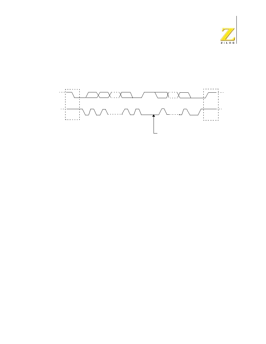
eZ80190 Product Specification
PS006611-0703
PRELIMINARY
I
2
C Serial I/O Interface
92
nificant bit (msb) first. See Figure 18. A receiver can hold the SCL line Low to
force the transmitter into a WAIT state. Data transfer then continues when the
receiver is ready for another byte of data and releases SCL.
Acknowledge
Data transfer with an ACK function is obligatory. The ACK-related clock pulse is
generated by the master. The transmitter releases the SDA line (High) during the
ACK clock pulse. The receiver must pull down the SDA line during the ACK clock
pulse so that it remains Low during the High period of this clock pulse. See
Figure 19.
A receiver that is addressed is obliged to generate an ACK after each byte is
received. When a slave receiver does not acknowledge the slave address (that is,
the slave receiver is unable to receive because it is performing some real-time
function), the data line must be left High by the slave. The master then generates
a STOP condition to abort the transfer.
If a slave receiver acknowledges the slave address, but cannot receive any more
data bytes, the master must abort the transfer. The abort is indicated by the slave
generating the Not Acknowledge (NACK) on the first byte to follow. The slave
leaves the data line High and the master generates the STOP condition.
If a master receiver is involved in a transfer, it must signal the end of the data
transfer to the slave transmitter by not generating an ACK on the final byte
clocked out of the slave. The slave transmitter must release the data line to allow
the master to generate a STOP or a repeated START condition.
Figure 18. I
2
C Frame Structure
SDA Signal
SCL Signal
MSB
S
Start Condition
1
2
8
9
Acknowledge
From Receiver
Clock Line Held Low By Receiver
1
Acknowledge
From Receiver
9
ACK
P
Stop Condition
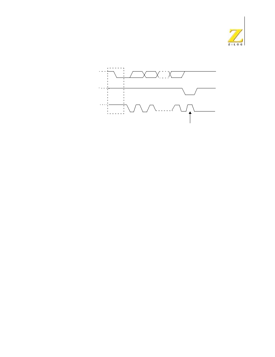
eZ80190 Product Specification
PS006611-0703
PRELIMINARY
I
2
C Serial I/O Interface
93
Clock Synchronization
All masters generate their own clocks on the SCL line to transfer messages on the
I
2
C bus. Data is only valid during the High period of each clock.
Clock synchronization is performed using the wired AND connection of the I
2
C
interfaces to the SCL line, meaning that a High-to-Low transition on the SCL line
causes the relevant devices to start counting from their Low period. When a
device clock goes Low, it holds the SCL line in that state until the clock High state
is reached. See Figure 20. The Low-to-High transition of this clock, however, may
not change the state of the SCL line if another clock still exists within its Low
period. The SCL line is held Low by the device with the longest Low period.
Devices with shorter Low periods enter a High WAIT state during this time.
When all devices complete counting off their Low periods, the clock line goes
High. There is no difference between the device clocks and the state of the SCL
line; therefore, all of the devices begin counting their High periods. The first device
to complete its High period again pulls the SCL line Low. In this way, a synchro-
nized SCL clock is generated with its Low period determined by the device with
the longest clock Low period, and its High period determined by the device with
the shortest clock High period.
Figure 19. I
2
C Acknowledge
Data Output by Transmitter
S
Start Condition
1
2
8
9
Clock Pulse for Acknowledge
Data Output by Receiver
SCL Signal From Master
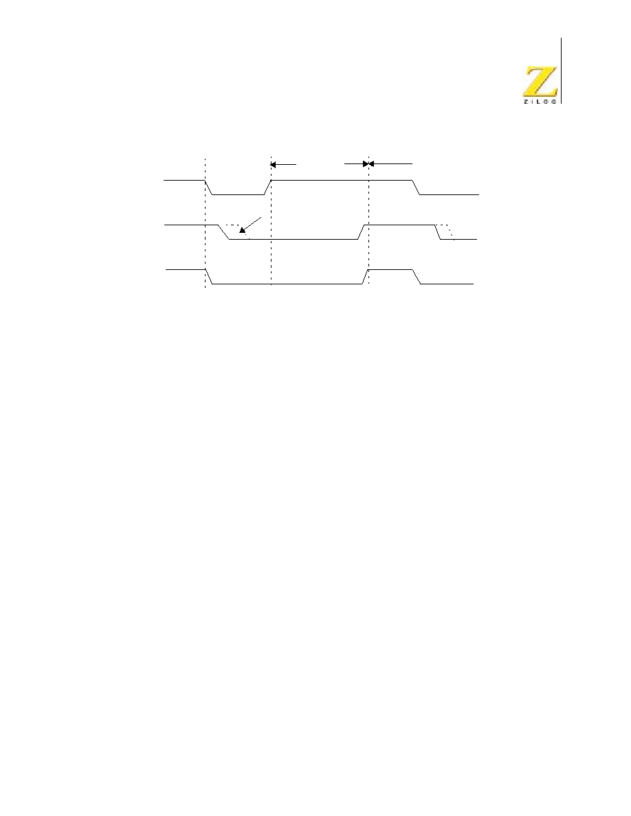
eZ80190 Product Specification
PS006611-0703
PRELIMINARY
I
2
C Serial I/O Interface
94
Arbitration
A master may start a transfer only if the bus is free. Two or more masters may
generate a START condition within the minimum hold time of the START condi-
tion. The result is a defined START condition to the bus. Arbitration occurs on the
SDA line while the SCL line is at the High level in such a way that the master,
(which transmits a High level while another master is transmitting a Low level),
switches off its data output stage. The master switches off its data output stage
because the level on the bus does not correspond to its own level.
Arbitration can continue for many bits. Its first stage is a comparison of the
address bits. If the masters are each trying to address the same device, arbitra-
tion continues with a comparison of the data. Because address and data informa-
tion on the I
2
C bus is used for arbitration, no information is lost during this
process. A master which loses the arbitration can generate clock pulses until the
end of the byte in which it loses the arbitration.
If a master also incorporates a slave function and it loses arbitration during the
addressing stage, it is possible that the winning master is trying to address it. The
losing master must switch over immediately to SLAVE RECEIVE mode. Figure 20
illustrates the arbitration procedure for two masters. Of course, more may be
involved (depending on how many masters are connected to the bus). The
moment there is a difference between the internal data level of the master gener-
ating DATA 1 and the actual level on the SDA line, its data output is switched off,
which means that a High output level is then connected to the bus. As a result, the
data transfer initiated by the winning master is not affected. Because control of the
I
2
C bus is decided solely on the address and data sent by competing masters,
there is no central master, nor any order of priority on the bus.
Special attention must be paid if, during a serial transfer, the arbitration procedure
is still in progress at the moment when a repeated START condition or a STOP
condition is transmitted to the I
2
C bus. If it is possible for such a situation to occur,
Figure 20. Clock Synchronization In I
2
C Protocol
Start Counting
High Period
Clk1 Signal
Clk2 Signal
SCL Signal
Counter
Reset
Wait State

eZ80190 Product Specification
PS006611-0703
PRELIMINARY
I
2
C Serial I/O Interface
95
the masters involved must send this repeated START condition or STOP condition
at the same position in the format frame. In other words, arbitration is not allowed
between:
∑
A repeated START condition and a data bit
∑
A STOP condition and a data bit
∑
A repeated START condition and a STOP condition
Clock Synchronization for Handshake
The Clock synchronizing mechanism can function as a handshake, enabling
receivers to cope with fast data transfers, on either a byte or bit level. The byte
level allows a device to receive a byte of data at a fast rate, but allows the device
more time to store the received byte or to prepare another byte for transmission.
Slaves hold the SCL line Low after reception and acknowledge the byte, forcing
the master into a WAIT state until the slave is ready for the next byte transfer in a
handshake procedure.
Operating Modes
Master Transmit
In MASTER TRANSMIT mode, the I
2
C transmits a number of bytes to a slave
receiver.
The device enters MASTER TRANSMIT mode by setting the Master Mode Start
bit (STA) bit in the I2Cx_CTL register to 1. The I
2
C then tests the I
2
C bus and
transmits a START condition when the bus is free. When a START condition is
transmitted, the IFLG bit is set to 1 and the status code in the I2Cx_SR register is
08h
. Before this interrupt is serviced, the I2Cx_DR register must be loaded with
either a 7-bit slave address or the first part of a 10-bit slave address, with the lsb
cleared to 0 to specify TRANSMIT mode. The IFLG bit should now be cleared to 0
to prompt the transfer to continue.
After the 7-bit slave address (or the first part of a 10-bit address) plus the write bit
are transmitted, the IFLG is set again. A number of status codes are possible in
the I2Cx_SR register.

eZ80190 Product Specification
PS006611-0703
PRELIMINARY
I
2
C Serial I/O Interface
96
If 10-bit addressing is being used, then the status code is
18h
or
20h
after the first
part of a 10-bit address, plus the write bit, are successfully transmitted.
After this interrupt is serviced and the second part of the 10-bit address is trans-
mitted, the I2Cx_SR register contains one of the codes in Table 44.
Table 43. I
2
C Master Transmit Status Codes
Code
I
2
C State
Microprocessor Response
Next I
2
C Action
18h
Addr+W transmitted,
ACK received
For a 7-bit address: Write a
byte to DATA, clear IFLG
Transmit data byte,
receive ACK
Or set STA, clear IFLG
Transmit repeated
START
Or set STP, clear IFLG
Transmit STOP
Or set STA & STP, clear IFLG Transmit STOP then
START
For a 10-bit address: write an
extended address byte to
DATA, clear IFLG
Transmit extended
address byte
20h
Addr+W transmitted,
ACK not received
Same as code 18h
Same as code 18h
38h
Arbitration lost
Clear IFLG
Return to the IDLE state
Or set STA, clear IFLG
Transmit START when
bus is free
68h
Arbitration lost,
SLA+W received, ACK
transmitted
Clear IFLG, ACK = 0
Receive data byte,
transmit NACK
Or clear IFLG, ACK = 1
Receive data byte,
transmit ACK
78h
Arbitration lost,
General call addr
received, ACK
transmitted
Same as code 68h
Same as code 68h
B0h
Arbitration lost, SLA+R
received, ACK
transmitted
Write byte to DATA, clear
IFLG, clear ACK = 0
Transmit last byte,
receive ACK
Or write byte to DATA, clear
IFLG, set ACK = 1
Transmit data byte,
receive ACK
Note: W = Write bit. The lsb is cleared to 0.

eZ80190 Product Specification
PS006611-0703
PRELIMINARY
I
2
C Serial I/O Interface
97
If a repeated START condition is transmitted, the status code is
10h
instead of
08h
. After each data byte is transmitted, the IFLG is set to 1 and one of the status
codes listed in Table 45 is contained in the I2Cx_SR register.
Table 44. I
2
C 10-Bit Master Transmit Status Codes
Code
I
2
C State
Microprocessor Response
Next I
2
C Action
38h
Arbitration lost
Clear IFLG
Return to the IDLE state
Or set STA, clear IFLG
Transmit START when
the bus is free
68h
Arbitration lost,
SLA+W received, ACK
transmitted
Clear IFLG, clear ACK = 0
Receive data byte,
transmit NACK
Or clear IFLG, set ACK=1
Receive data byte,
transmit ACK
B0h
Arbitration lost, SLA+R
received, ACK
transmitted
Write byte to DATA, clear
IFLG, clear ACK = 0
Transmit last byte,
receive ACK
Or write byte to DATA, clear
IFLG, set ACK = 1
Transmit data byte,
receive ACK
D0h
Second Address byte
+ W transmitted, ACK
received
Write byte to DATA, clear IFLG Transmit data byte,
receive ACK
Or set STA, clear IFLG
Transmit repeated
START
Or set STP, clear IFLG
Transmit STOP
Or set STA & STP, clear IFLG Transmit STOP then
START
D8h
Second Address byte
+ W transmitted, ACK
not received
Same as code D0h
Same as code D0h
Table 45. I
2
C Master Transmit Status Codes For Data Bytes
Code
I
2
C State
Microprocessor Response
Next I
2
C Action
28h
Data byte transmitted,
ACK received
Write byte to DATA, clear IFLG Transmit data byte,
receive ACK
Or set STA, clear IFLG
Transmit repeated
START
Or set STP, clear IFLG
Transmit STOP
Or set STA & STP, clear IFLG Transmit START then
STOP
30h
Data byte transmitted,
ACK not received
Same as code 28h
Same as code 28h

eZ80190 Product Specification
PS006611-0703
PRELIMINARY
I
2
C Serial I/O Interface
98
When all bytes are transmitted, the microprocessor should write a 1 to the Master
Mode Stop bit (STP) bit in the I2Cx_CTL register. The I
2
C then transmits a STOP
condition, clears the STP bit, and returns to the IDLE state.
Master Receive
In MASTER RECEIVE mode, the I
2
C receives a number of bytes from a slave
transmitter.
After the START condition is transmitted, the IFLG bit is set to 1 and the status
code
08h
is loaded in the I2Cx_SR register. The I2Cx_DR register should be
loaded with the slave address (or the first part of a 10-bit slave address), with the
lsb set to 1 to signify a READ. The IFLG bit should be cleared to 0 as a prompt for
the transfer to continue.
When the 7-bit slave address (or the first part of a 10-bit address) and the read bit
are transmitted, the IFLG bit is set and one of the status codes listed in Table 46 is
contained in the I2Cx_SR register.
38h
Arbitration lost
Clear IFLG
Return to the IDLE state
Or set STA, clear IFLG
Transmit START when
bus free
Table 46. I
2
C Master Receive Status Codes
Code
I
2
C State
Microprocessor Response
Next I
2
C Action
40h
Addr + R transmitted,
ACK received
For a 7-bit address, clear IFLG,
ACK = 0
Receive data byte,
transmit NACK
Or clear IFLG, ACK = 1
Receive data byte,
transmit ACK
For a 10-bit address, write
extended address byte to
DATA, clear IFLG
Transmit extended
address byte
Note: R = Read bit. The lsb is set to 1.
Table 45. I
2
C Master Transmit Status Codes For Data Bytes (Continued)
Code
I
2
C State
Microprocessor Response
Next I
2
C Action

eZ80190 Product Specification
PS006611-0703
PRELIMINARY
I
2
C Serial I/O Interface
99
If 10-bit addressing is being used, the slave is first addressed using the full 10-bit
address plus the Write bit. The master then issues a restart followed by the first
part of the 10-bit address again, but with the READ bit. The status code is then
40h
or
48h
. The slave remains selected prior to the restart.
If a repeated START condition is received, the status code is
10h
instead of
08h
.
After each data byte is received, the IFLG is set and one of the status codes listed
in Table 47 is contained in the I2Cx_SR register.
48h
Addr + R transmitted,
ACK not received
For a 7-bit address: set STA,
clear IFLG
Transmit repeated
START
Or set STP, clear IFLG
Transmit STOP
Or set STA & STP, clear IFLG Transmit STOP then
START
For a 10-bit address: Write
extended address byte to
DATA, clear IFLG
Transmit extended
address byte
38h
Arbitration lost
Clear IFLG
Return to the IDLE state
Or set STA, clear IFLG
Transmit START when
bus is free
68h
Arbitration lost,
SLA+W received, ACK
transmitted
Clear IFLG, clear ACK = 0
Receive data byte,
transmit NACK
Or clear IFLG, set ACK = 1
Receive data byte,
transmit ACK
78h
Arbitration lost,
General call addr
received, ACK
transmitted
Same as code 68h
Same as code 68h
B0h
Arbitration lost, SLA+R
received, ACK
transmitted
Write byte to DATA, clear
IFLG, clear ACK = 0
Transmit last byte,
receive ACK
Or write byte to DATA, clear
IFLG, set ACK = 1
Transmit data byte,
receive ACK
Table 46. I
2
C Master Receive Status Codes (Continued)
Code
I
2
C State
Microprocessor Response
Next I
2
C Action
Note: R = Read bit. The lsb is set to 1.

eZ80190 Product Specification
PS006611-0703
PRELIMINARY
I
2
C Serial I/O Interface
100
When all bytes are received, a NACK is sent. Next, the microprocessor writes a 1
to the STP bit in the I2Cx_CTL register. The I
2
C then transmits a STOP condition,
clears the STP bit, and returns to the IDLE state.
Slave Transmit
In SLAVE TRANSMIT mode, a number of bytes are transmitted to a master
receiver. The I
2
C enters SLAVE TRANSMIT mode when it receives its own slave
address and a read bit after a START condition. The I
2
C then transmits an I
2
C
Acknowledge bit (ACK) if it is set to 1, and sets the IFLG bit in the I2Cx_CTL reg-
ister. The I2Cx_SR register contains the status code
A8h
.
When the I
2
C contains a 10-bit slave address (signified by
F0h≠F7h
in the
I2Cx_SAR register), it transmits an ACK after the first address byte is
received after a restart. An interrupt is generated, IFLG is set; however,
the status does not change. No second address byte is sent by the master.
The slave remains selected prior to the restart.
I
2
C goes from MASTER mode to SLAVE TRANSMIT mode when arbitration is lost
during the transmission of an address, and the slave address and read bit are
received. This action is confirmed by the status code
B0h
in the I2Cx_SR register.
The data byte to be transmitted is loaded into the I2Cx_DR register and the IFLG
bit is cleared. After the I
2
C transmits the byte and receives an ACK, the IFLG bit is
set and the I2Cx_SR register contains
B8h
. After the last byte to be transmitted is
loaded into the I2Cx_DR register, the ACK bit is cleared when the IFLG is cleared.
After the last byte is transmitted, the IFLG is set and the I2Cx_SR register con-
tains
C8h
. The I
2
C returns to the IDLE state. The ACK bit must be set to 1 before
SLAVE mode can be reentered.
Table 47. I
2
C Master Receive Status Codes For Data Bytes
Code
I
2
C State
Microprocessor Response
Next I
2
C Action
50h
Data byte received,
ACK transmitted
Read DATA, clear IFLG, clear
ACK = 0
Receive data byte,
transmit NACK
Or read DATA, clear IFLG, set
ACK = 1
Receive data byte,
transmit ACK
58h
Data byte received,
NACK transmitted
Read DATA, set STA, clear
IFLG
Transmit repeated
START
Or read DATA, set STP, clear
IFLG
Transmit STOP
Or read DATA, set STA & STP,
clear IFLG
Transmit STOP then
START
38h
Arbitration lost in
NACK bit
Same as master transmit
Same as master transmit
Note:

eZ80190 Product Specification
PS006611-0703
PRELIMINARY
I
2
C Serial I/O Interface
101
If no ACK is received after transmitting a byte, the IFLG is set and the I2Cx_SR
register contains
C0h
. The I
2
C then returns to the IDLE state.
If a STOP condition is detected after an ACK bit, the I
2
C returns to the IDLE state.
Slave Receive
In SLAVE RECEIVE mode, a number of data bytes are received from a master
transmitter.
The I
2
C enters SLAVE RECEIVE mode when it receives its own slave address
and a write bit (lsb = 0) after a START condition. The I
2
C transmits an ACK bit and
sets the IFLG bit in the I2Cx_CTL register. The I2Cx_SR register then contains
the status code
60h
. The I
2
C also enters SLAVE RECEIVE mode when it receives
the general call address
00h
(if the GCE bit in the I2Cx_SAR register is set). The
status code is then
70h
.
When the I
2
C contains a 10-bit slave address (signified by
F0h≠F7h
in the
I2Cx_SAR register), it transmits an ACK after the first address byte is
received; however, no interrupt is generated. IFLG is not required to be set
and the status does not change. The I
2
C generates an interrupt only after
the second address byte is received. The I
2
C then sets the IFLG bit and
loads the status code, as described above.
I
2
C goes from MASTER mode to SLAVE RECEIVE mode when arbitration is lost
during the transmission of an address, and the slave address and write bit (or the
general call address if the CGE bit in the I2Cx_SAR register is set to 1) are
received. The status code in the I2Cx_SR register is
68h
if the slave address is
received or
78h
if the general call address is received. The IFLG bit must be
cleared to 0 to allow data transfer to continue.
If the ACK bit in the I2Cx_CTL register is set to 1, then an ACK bit (Low level on
SDA) is transmitted and the IFLG bit is set after each byte is received. The
I2Cx_SR register contains the status code
80h
or
90h
if SLAVE RECEIVE mode
is entered with the general call address. The received data byte can be read from
the I2Cx_DR register and the IFLG bit must be cleared to allow the transfer to
continue. If a STOP condition or a repeated START condition is detected after the
ACK bit, the IFLG bit is set and the I2Cx_SR register contains status code
A0h
.
If the ACK bit is cleared to 0 during a transfer, the I
2
C transmits a NACK bit (High
level on SDA) after the next byte is received, and sets the IFLG bit. The I2Cx_SR
register contains the status code
88h
or
98h
if SLAVE RECEIVE mode is entered
with the general call address. The I
2
C returns to the IDLE state when the IFLG bit
is cleared to 0.
Note:

eZ80190 Product Specification
PS006611-0703
PRELIMINARY
I
2
C Serial I/O Interface
102
I
2
C Registers
Addressing
The processor interface provides access to six 8-bit registers: four Read/Write
registers, one Read Only register, and two Write Only registers. See Table 48.
Resetting the I
2
C Registers
Hardware Reset.
When the I
2
C is reset by a hardware reset of the eZ80190
device, the I2Cx_SAR, I2Cx_xSAR, I2Cx_DR and I2Cx_CTL registers are
cleared to
00h
. The
I2Cx_SR register is set to
F8h
.
Software Reset.
Perform a software reset by writing any value to the I
2
C Software
Reset register (I2Cx_SRR). A software reset sets the I
2
C back to the IDLE state
and the STP, STA, and IFLG bits of the I2Cx_CTL register to 0.
I
2
C Slave Address Register
The I2Cx_SAR register, indicated in Table 49, provides the 7-bit address of the
I
2
C when in SLAVE mode and allows 10-bit addressing in conjunction with the
I2Cx_xSAR register. I2Cx_SAR[7:1] = SLA[6:0] is the 7-bit address of the I
2
C
when in 7-bit SLAVE mode. When the I
2
C receives this address after a START
condition, it enters SLAVE mode. I2Cx_SAR[7] corresponds to the first bit
received from the I
2
C bus.
When the register receives an address starting with
F7h
to
F0h
(I2Cx_SAR[7:3] =
11110b
), the I
2
C recognizes that a 10-bit slave addressing mode is being
selected. The I
2
C sends an ACK after receiving the I2Cx_SAR byte (the device
does not generate an interrupt at this point). After the next byte of the address
(I2Cx_xSAR) is received, the I
2
C generates an interrupt and enters SLAVE mode.
Table 48. I
2
C Register Descriptions
Register
Description
I2Cx_SAR
Slave address register
I2Cx_xSAR
Extended slave address register
I2Cx_DR
Data byte register
I2Cx_CTL
Control register
I2Cx_SR
Status register (Read Only)
I2Cx_CCR
Clock Control register (Write Only)
I2Cx_SRR
Software reset register (Write Only)
Note: The lower case x in the register name can be either 0 or 1 depending upon which of the two
I
2
C devices are referenced within the eZ80190 device.

eZ80190 Product Specification
PS006611-0703
PRELIMINARY
I
2
C Serial I/O Interface
103
Then I2Cx_SAR[2:1] is used as the upper 2 bits of the 10-bit extended address.
The full 10-bit address is returned by {I2Cx_SAR[2:1], I2Cx_xSAR[7:0]}.
I
2
C Extended Slave Address Register
The I2Cx_xSAR register, indicated in Table 50, is used in conjunction with the
I2Cx_SAR register to provide 10-bit addressing for the I
2
C when in SLAVE mode.
The I2Cx_SAR value forms the lower 8 bits of the 10-bit slave address. The full
10-bit address is returned by {I2Cx_SAR[2:1], I2Cx_xSAR[7:0]}.
When the register receives an address starting with
F7h
to
F0h
(I2Cx_SAR[7:3] =
11110b
), the I
2
C recognizes that a 10-bit slave addressing mode is being
selected. The I
2
C sends an ACK after receiving the I2Cx_SAR byte (the device
does not generate an interrupt at this point). After the next byte of the address
(I2Cx_xSAR) is received, the I
2
C generates an interrupt and enters SLAVE mode.
Then I2Cx_SAR[2:1] is used as the upper 2 bits of the 10-bit extended address.
The full 10-bit address is returned by {I2Cx_SAR[2:1], I2Cx_xSAR[7:0]}.
Table 49. I
2
C Slave Address Registers
(I2C0_SAR = C8h, I2C1_SAR = D8h)
Bit
7
6
5
4
3
2
1
0
Reset
0
0
0
0
0
0
0
0
CPU Access
R/W
R/W
R/W
R/W
R/W
R/W
R/W
R/W
Note: R/W = Read/Write.
Bit
Position
Value
Description
[7:1]
SLA
00h≠
7Fh
The 7-bit slave address, or the lower 7 bits of the slave
address, when operating in 10-bit mode.
0
GCE
0
The I
2
C is not enabled to recognize the General Call Address.
1
The I
2
C is enabled to recognize the General Call Address.
eZ80190 Product Specification
PS006611-0703
PRELIMINARY
I
2
C Serial I/O Interface
104
I
2
C Data Register
The I
2
C Data Register, indicated in Table 51, contains the data byte/slave address
to be transmitted or the data byte just received. In MASTER TRANSMIT or
SLAVE TRANSMIT modes, the most significant bit of the byte is transmitted first.
In MASTER RECEIVE or SLAVE RECEIVE modes, the first bit received is placed
in the most significant bit of the register. After each byte is transmitted, the
I2Cx_DR register contains the byte that is present in the event of lost arbitration.
I
2
C Control Register
The I2Cx_CTL register, indicated in Table 52 is a control register that is used to
control the interrupts and the master slave relationships on the I
2
C bus.
When the Interrupt Enable bit (IEN) is set to 1, the interrupt line goes High when
the IFLG is set to 1. When IEN is cleared to 0, the interrupt line always remains
Low.
Table 50. I
2
C Extended Slave Address Registers
(I2C0_xSAR
=
C9h, I2C1_xSAR
=
D9h)
Bit
7
6
5
4
3
2
1
0
Reset
0
0
0
0
0
0
0
0
CPU Access
R/W
R/W
R/W
R/W
R/W
R/W
R/W
R/W
Note: R/W = Read/Write.
Bit
Position
Value
Description
[7:0]
SLAX
00h≠
FFh
Least significant 8 bits of the 10-bit extended slave address.
Table 51. I
2
C Data Registers
(I2C0_DR = CAh, I2C1_DR = DAh)
Bit
7
6
5
4
3
2
1
0
Reset
0
0
0
0
0
0
0
0
CPU Access
R/W
R/W
R/W
R/W
R/W
R/W
R/W
R/W
Note: R/W = Read/Write.
Bit
Position
Value
Description
[7:0]
DATA
00h≠
FFh
I
2
C data byte.

eZ80190 Product Specification
PS006611-0703
PRELIMINARY
I
2
C Serial I/O Interface
105
When the Bus Enable bit (ENAB) is set to 0, the I
2
C bus inputs SCLx. SDAx is
ignored and the I
2
C module does not respond to any address on the bus. When
ENAB is set to 1, the I
2
C responds to calls to its slave address and to the general
call address if the GCE bit (I2Cx_SAR[0]) is set to 1.
When the Master Mode Start bit (STA) is set to 1, the I
2
C enters MASTER mode
and sends a START condition on the bus when the bus is free. If the STA bit is set
to 1 when the I
2
C module is already in MASTER mode and one or more bytes are
transmitted, then a repeated START condition is sent. If the STA bit is set to 1
when the I
2
C block is being accessed in SLAVE mode, the I
2
C completes the data
transfer in SLAVE mode and then enters MASTER mode when the bus is
released. The STA bit is automatically cleared after a START condition is set.
Writing a 0 to this bit produces no effect.
If the Master Mode Stop bit (STP) is set to 1 in MASTER mode, a STOP condition
is transmitted on the I
2
C bus. If the STP bit is set to 1 in SLAVE mode, the I
2
C
module behaves as if a STOP condition is received, but no STOP condition is
transmitted. If both STA and STP bits are set, the I
2
C block first transmits the
STOP condition (if in MASTER mode) and then transmits the START condition.
The STP bit is cleared automatically. Writing a 0 to this bit produces no effect.
The I
2
C Interrupt Flag (IFLG) is set to 1 automatically when the device enters any
of 30 of the possible 31 I
2
C states. The only state that does not set the IFLG bit is
state
F8h
. If IFLG is set to 1 and the IEN bit is also set to 1, an interrupt is gener-
ated. When IFLG is set by the I
2
C, the Low period of the I
2
C bus clock line is
stretched and the data transfer is suspended. When a 0 is written to IFLG, the
interrupt is cleared and the I
2
C clock line is released.
When the I
2
C Acknowledge bit (ACK) is set to 1, an acknowledgement is sent dur-
ing the Acknowledge clock pulse on the I
2
C bus if:
∑
Either the whole of a 7-bit slave address or the first or second byte of a 10-bit
slave address is received
∑
The general call address is received and the General Call Enable bit in
I2Cx_SAR is set to 1
∑
A data byte is received in MASTER or SLAVE mode
When ACK is cleared to 0, a NACK is sent when a data byte is received in MAS-
TER or SLAVE mode. If ACK is cleared to 0 in SLAVE TRANSMIT mode, the byte
in the I2Cx_DR register is presumed to be the last byte. After this byte is transmit-
ted, the I
2
C block enters state
C8h
, then returns to the IDLE state. The I
2
C module
does not respond to its slave address unless ACK is set.

eZ80190 Product Specification
PS006611-0703
PRELIMINARY
I
2
C Serial I/O Interface
106
Table 52. I
2
C Control Registers
(I2C0_CTL = CBh, I2C1_CTL = DBh)
Bit
7
6
5
4
3
2
1
0
Reset
0
0
0
0
0
0
0
0
CPU Access
R/W
R/W
R/W
R/W
R/W
R/W
R/W
R/W
Note: R/W = Read/Write.
Bit
Position
Value
Description
7
IEN
0
I
2
C interrupt is disabled.
1
I
2
C interrupt is enabled.
6
ENAB
0
The I
2
C bus (SCLx/SDAx) is disabled and all inputs are
ignored.
1
The I
2
C bus (SCLx/SDAx) is enabled.
5
STA
0
A Master Mode START condition is sent.
1
A Master Mode START TRANSMIT condition occurs on the
bus.
4
STP
0
A Master Mode STOP condition is sent.
1
A Master Mode STOP TRANSMIT condition occurs on the
bus.
3
IFLG
0
The I
2
C interrupt flag is not set.
1
The I
2
C interrupt flag is set.
2
ACK
0
Not Acknowledge.
1
Acknowledge.
[1:0]
00
Reserved.

eZ80190 Product Specification
PS006611-0703
PRELIMINARY
I
2
C Serial I/O Interface
107
I
2
C Status Register
The I2Cx_SR register, indicated in Table 53, is a Read Only register that contains
a 5-bit status code in the five most significant bits. The three least significant bits
are always 0. The Read Only I2Cx_SR registers share the same I/O addresses as
the Write Only I2Cx_CCR registers.
There are 29 possible status codes, indicated in Table 54. When the I2Cx_SR
register contains the status code
F8h
, no relevant status information is available,
no interrupt is generated and the IFLG bit in the I2Cx_CTL register is not set. All
other status codes correspond to a defined state of the I
2
C.
When the device enters each of these states, the corresponding status code
appears in this register and the IFLG bit in the I2Cx_CTL register is set. When the
IFLG bit is cleared, the status code returns to
F8h
.
Table 53. I
2
C Status Registers
(I2C0_SR = CCh, I2C1_SR = DCh)
Bit
7
6
5
4
3
2
1
0
Reset
1
1
1
1
1
0
0
0
CPU Access
R
R
R
R
R
R
R
R
Note: R = Read Only.
Bit
Position
Value
Description
[7:3]
STAT
00000≠
11111
5-bit I
2
C status code.
[2:0]
000
Reserved.
Table 54. I
2
C Status Codes
Code
Status
00h
Bus error
08h
START condition transmitted
10h
Repeated START condition transmitted
18h
Address + write bit transmitted, ACK received
20h
Address + write bit transmitted, ACK not received
28h
Data byte transmitted in MASTER mode, ACK received
30h
Data byte transmitted in MASTER mode, ACK not received
38h
Arbitration lost in address or data byte
40h
Address + read bit transmitted, ACK received

eZ80190 Product Specification
PS006611-0703
PRELIMINARY
I
2
C Serial I/O Interface
108
If an illegal condition occurs on the I
2
C bus, the bus error state is entered (status
code
00h
). To recover from this state, the STP bit in the I2Cx_CTL register must
be set and the IFLG bit cleared. The I
2
C then returns to the IDLE state. No STOP
condition is transmitted on the I
2
C bus.
The STP and STA bits may be simultaneously set to 1 to recover from the
bus error. The I
2
C then sends a START.
I
2
C Clock Control Register
The I2Cx_CCR register, indicated in Table 55, is a Write Only register. The seven
LSBs control the frequency at which the I
2
C bus is sampled and the frequency of
the I
2
C clock line (SCL) when the I
2
C is operating in MASTER mode. The Write
48h
Address + read bit transmitted, ACK not received
50h
Data byte received in MASTER mode, ACK transmitted
58h
Data byte received in MASTER mode, NACK transmitted
60h
Slave address + write bit received, ACK transmitted
68h
Arbitration lost in address as master, slave address + write bit received, ACK
transmitted
70h
General Call address received, ACK transmitted
78h
Arbitration lost in address as master, General Call address received, ACK
transmitted
80h
Data byte received after slave address received, ACK transmitted
88h
Data byte received after slave address received, NACK transmitted
90h
Data byte received after General Call received, ACK transmitted
98h
Data byte received after General Call received, NACK transmitted
A0h
STOP or repeated START condition received in SLAVE mode
A8h
Slave address + read bit received, ACK transmitted
B0h
Arbitration lost in address as master, slave address + read bit received, ACK
transmitted
B8h
Data byte transmitted in SLAVE mode, ACK received
C0h
Data byte transmitted in SLAVE mode, ACK not received
C8h
Last byte transmitted in SLAVE mode, ACK received
D0h
Second Address byte + write bit transmitted, ACK received
D8h
Second Address byte + write bit transmitted, ACK not received
F8h
No relevant status information, IFLG = 0
Table 54. I
2
C Status Codes (Continued)
Code
Status
Note:

eZ80190 Product Specification
PS006611-0703
PRELIMINARY
I
2
C Serial I/O Interface
109
Only I2Cx_CCR registers share the same I/O addresses as the Read Only
I2Cx_SR registers.
The I
2
C clocks are derived by the eZ80190 device's system clock, which provides
a frequency of f
sclk
. The I
2
C bus is sampled by the I
2
C block at the frequency
f
samp
in the following equation.
In MASTER mode, the I
2
C clock output frequency on SCLx (f
scl
) is provided by:
The use of two separately-programmable dividers allows the MASTER mode out-
put frequency to be set independently of the frequency at which the I
2
C bus is
sampled. These dividers are particularly useful in multimaster systems because
the I
2
C bus sampling frequency must be at least 10 times the frequency of the
fastest master on the bus to ensure that START and STOP conditions are always
detected. By using two programmable clock divider stages, a high sampling fre-
quency can be ensured, while allowing the MASTER mode output to be set to a
lower frequency.
Table 55. I
2
C Clock Control Registers
(I2C0_CCR = CCh, I2C1_CCR = DCh)
Bit
7
6
5
4
3
2
1
0
Reset
0
0
0
0
0
0
0
0
CPU Access
W
W
W
W
W
W
W
W
Note: W = Read Only.
Bit
Position
Value
Description
7
0
Reserved.
[6:3]
M
0000≠
1111
I
2
C clock divider scalar value.
[2:0]
N
000≠111 I
2
C clock divider exponent.
f
SAMP
=
f
SCLK
2
N
f
SCL
=
f
SCLK
10 x (M+1) x 2
N

eZ80190 Product Specification
PS006611-0703
PRELIMINARY
I
2
C Serial I/O Interface
110
Bus Clock Speed
The I
2
C bus is defined for bus clock speeds up to 100 kbps (400 kbps in FAST
mode).
To ensure correct detection of START and STOP conditions on the bus, the I
2
C
must sample the I
2
C bus at least ten times faster than the bus clock speed of the
fastest master on the bus. The sampling frequency should therefore be at least 1
MHz (4 MHz in FAST mode) to guarantee correct operation with other bus mas-
ters.
The I
2
C sampling frequency is determined by the frequency of the eZ80190
device system clock and the value in the I2Cx_CCR bits 2 to 0. The bus clock
speed generated by the I
2
C in MASTER mode is determined by the frequency of
the input clock and the values in I2Cx_CCR[2:0] and I2Cx_CCR[6:3].
I
2
C Software Reset Register
The I2Cx_SRR register, indicated in Table 56, is a Write Only register. Writing any
value to this register will perform a software reset of the I
2
C module.
Table 56. I
2
C Software Reset Register
(I2C0_SRR = CDh, I2C1_SRR = DDh)
Bit
7
6
5
4
3
2
1
0
Reset
X
X
X
X
X
X
X
X
CPU Access
W
W
W
W
W
W
W
W
Note: W = Write Only.
Bit
Position
Value
Description
[7:0]
SRR
00h≠FFh Writing any value to this register performs a software reset of
the I
2
C module.

eZ80190 Product Specification
PS006611-0703
PRELIMINARY
Multiply-Accumulator
111
Multiply-Accumulator
MACC Overview
The most significant process in digital signal processing is the Multiply-Accumu-
late (MACC) function, which forms a sum of products, as the following equation
shows.
where x and y are vectors (tables of values, one-dimensional arrays) in memory.
The MACC block on the eZ80190 device performs DSP functions without incur-
ring the control overhead costs associated with a separate DSP.
Features include:
∑
Two 40-bit accumulators
∑
A 16-bit x 16-bit multiplier with a 32-bit product
≠
The 32-bit output is added to the value stored in 1 of the 2 available 40-bit
accumulators
≠
The 40-bit sum is written back to the selected 40-bit accumulator
∑
Each multiply-accumulate operation completes in a single clock cycle
∑
Two 256 x 16 dual-port RAM spaces labeled x and y
≠
One port of each RAM is 16-bit Read Only and feeds the multiplier
≠
The second port is 8-bit Read/Write and is connected to the CPU data
bus, allowing the dual RAM to be part of the CPU memory space
∑
A set of control registers in the CPU's I/O space are used to set up the next
multiply-accumulate operation, initiate the operation, determine when the
Multiply-Accumulator completes the current calculation, and retrieve the result
A simplified block diagram of the Multiply-Accumulator is illustrated in Figure 21.
x
i
y
i
◊
i
n
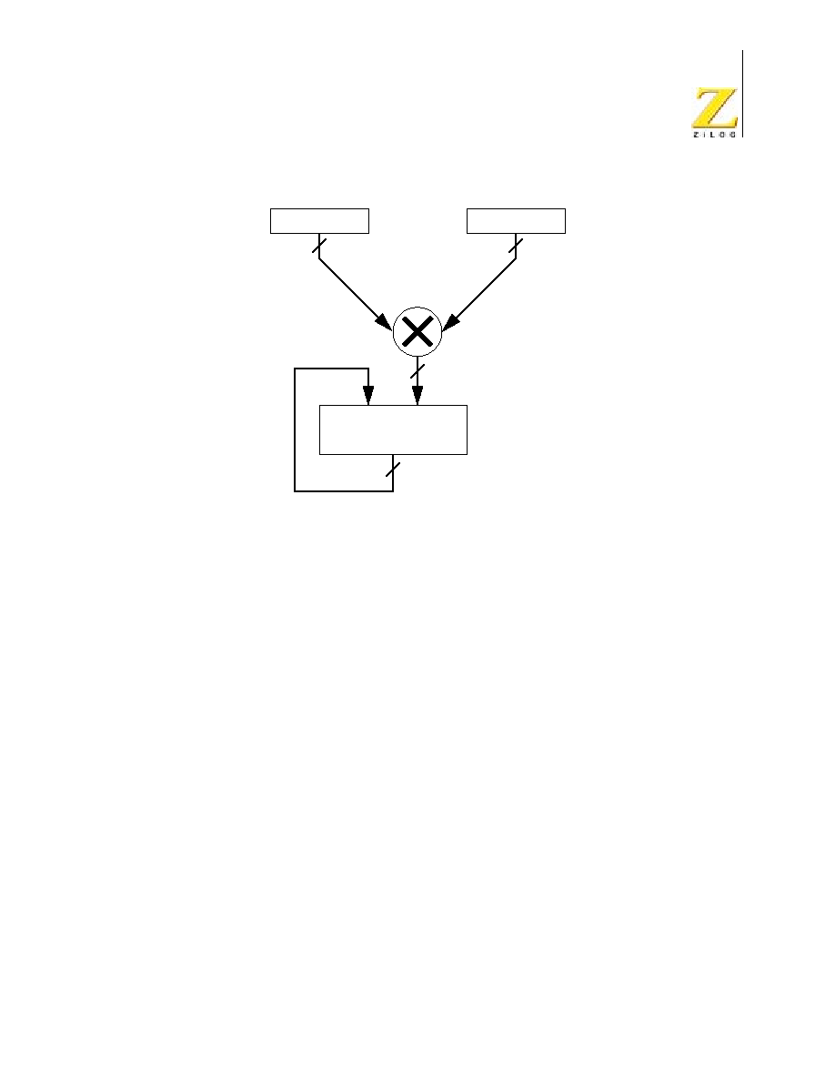
eZ80190 Product Specification
PS006611-0703
PRELIMINARY
Multiply-Accumulator
112
Multiply-Accumulator Basic Operation
Figure 22 demonstrates a simplified view of the state progression of the MACC
when performing calculation on a set of data. The progression begins in the upper
left corner with a DATA bank containing the value EMPTY. The CPU loads the
MACC control registers to define the next MACC calculation.
If the MACC is not busy with an existing calculation (EMPTY or DONE), the DATA
and CALC banks are immediately swapped to initiate the new calculation. If the
MACC is busy with an existing calculation, the DATA bank status changes to
READY and waits for the MACC to complete the existing calculation. Then, the
DATA and CALC banks are swapped to initiate the new calculation.
Assuming the DATA bank is EMPTY or READY when the MACC completes the
new calculation, the CALC bank is swapped with the DATA bank. The CPU can
then retrieve the result of the new calculation from the accumulator.
Figure 21. Multiply-Accumulator Block Diagram
x DATA
y DATA
40-Bit
Accumulator
16
16
32
40
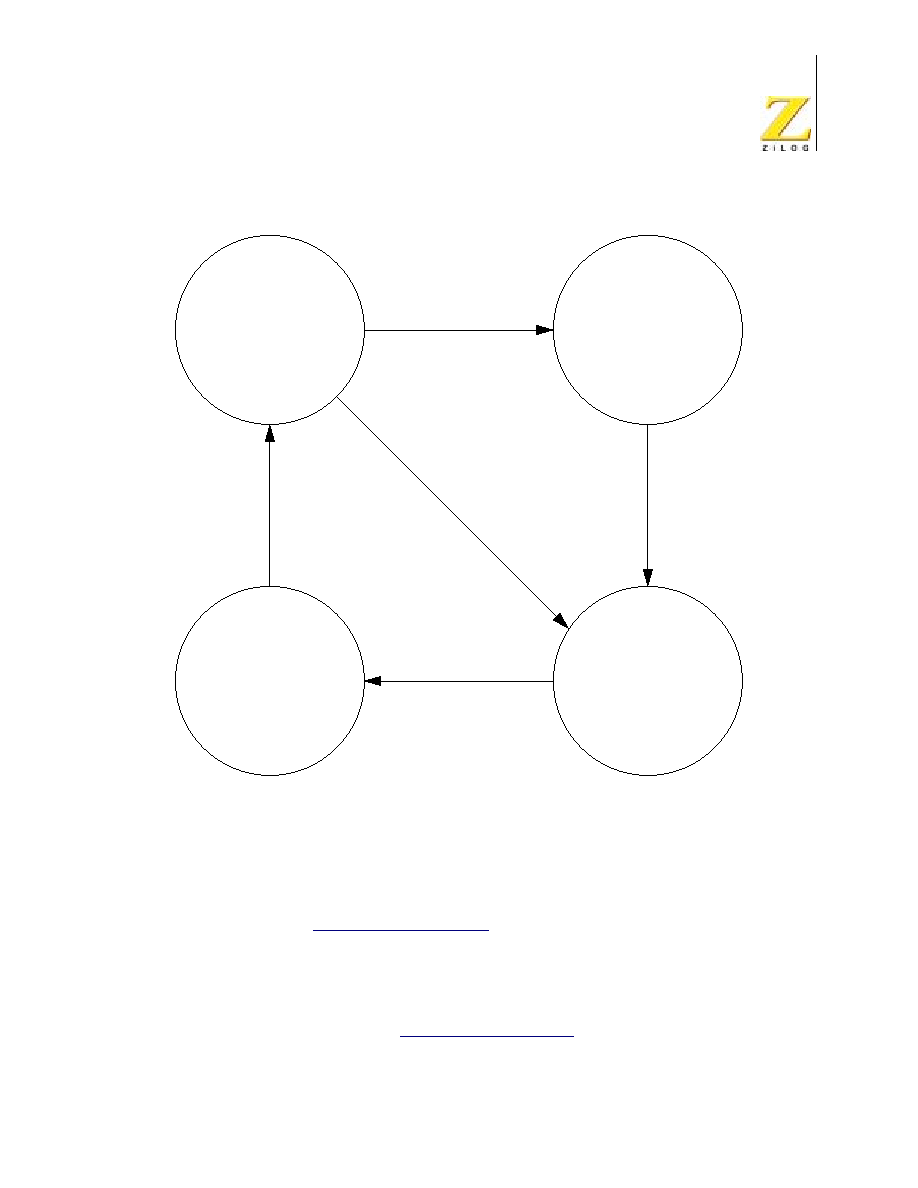
eZ80190 Product Specification
PS006611-0703
PRELIMINARY
Multiply-Accumulator
113
Software Control of the MACC
The Multiply-Accumulator is designed so that CPU software can set up a calcula-
tion by writing to the MACC registers using a single OTI2R block output instruc-
tion. See the
eZ80 CPU User Manual
for details. Depending upon the calculation
required, this calculation may require writing to all of the MACC control registers,
or just a partial subset.
Similarly, the MACC is designed so that eZ80
Æ
CPU software can read the results
of a calculation from the MACC Accumulator registers using a single INI2R block
input instruction. See the
eZ80 CPU User Manual
for details. Depending upon the
number of bytes of result required, the INI2R instruction can read all 5 of the
MACC_ACx registers or as few as 1.
Figure 22. Simplified MACC Status Progression
CALC Bank
IN PROGRESS
DATA Bank swapped
with CALC Bank.
MACC begins
calculation.
DATA Bank
READY
Waiting for MACC
to complete current
calculation.
DATA Bank
DONE
CALC Bank swapped
with DATA Bank.
Result ready
in accumulator.
DATA Bank
EMPTY
The eZ80 can
define a new .
calculation for the
MACC.
Load DATA Bank
Registers
MACC completes
operation with
CALC Bank.
CALC Bank
EMPTY or DONE
Load DATA Bank
Registers
CALC Bank
IN PROGRESS
MACC completes
operation with
CALC Bank.
DATA Bank
READY
Read DATA Bank
Accumulator

eZ80190 Product Specification
PS006611-0703
PRELIMINARY
Multiply-Accumulator
114
The Multiply-Accumulator decodes its I/O addresses from ADDR[7:0]. In addition,
it monitors ADDR[15:8] to detect the final transfer of a block using the OTI2R or
INI2R instructions. These instructions drive the value in the CPU's B register onto
ADDR[15:8] and the value in the CPU's C register onto ADDR[7:0]. The B register
decrements after completion of each transfer in the OTI2R or INI2R block transfer.
The C register increments after completion of each transfer. The final transfer
occurs when B contains the value of
01h
. After this final transfer, B decrements to
0 and the block instruction terminates. Refer to the
eZ80 CPU User Manual
for
more information on these CPU instructions and CPU registers.
Defining A New Calculation As READY
When writing a new calculation to the MACC control registers, any of the following
actions change the state of the DATA bank from EMPTY to READY:
∑
A write to MACC_AC4, the most significant byte of the MACC Accumulator.
∑
A write to MACC_CTL with ADDR[15:8] =
01h
(an OTI2R instruction satisfies
this write requirement during its final transfer)
≠
This write also clears the MACC Accumulator
∑
A write to MACC_AC0, MACC_AC1, MACC_AC2, or MACC_AC3 with
ADDR[15:8] =
01h
(an OTI2R instruction satisfies this write requirement
during its final transfer)
If the MACC is prepared to begin a new calculation (CALC bank status is EMPTY
or DONE), the banks are immediately swapped as soon as the new calculation
defined in the DATA bank is READY. When this swap occurs, the CALC bank sta-
tus becomes IN PROGRESS.
Defining The DATA Bank As EMPTY
Defining the DATA Bank as EMPTY indicates completion of a result read opera-
tion. When reading a result from the MACC Accumulator registers, any of the fol-
lowing actions change the state of the DATA bank from DONE to EMPTY:
∑
A read from MACC_AC4, the most significant byte of the MACC Accumulator
∑
A read from MACC_AC0, MACC_AC1, MACC_AC2, or MACC_AC3 with
ADDR[15:8] =
01h
, as in the final transfer, using an INI2R instruction
Alternatively, any write operation to any of the MACC registers besides
MACC_STAT also changes the DATA bank status from DONE to EMPTY. This
state change occurs because write operations generally indicate a requirement to
define a new calculation.

eZ80190 Product Specification
PS006611-0703
PRELIMINARY
Multiply-Accumulator
115
Alternatives to OTI2R and INI2R
The INI2R and OTI2R instructions are recommended for CPU input and output
access to the MACC control registers. However, it is not required that only these
instructions be employed. Other I/O instructions can also be used.
Care must be taken to ensure that the High byte of the I/O address,
ADDR[15:8], is only set to
01h
when a state change is required on the
MACC DATA and CALC banks.
MACC Dual Bank Operation
The Multiply-Accumulator is divided into two separate operating banks. As a
result, one bank of the MACC performs a set of multiply-accumulate operations
on a set of data while the eZ80190 device is preparing the other bank for the next
set of multiply-accumulate operations. Each bank features a separate accumula-
tor and a separate set of control register values (MACC_xSTART, MACC_xEND,
MACC_xRELOAD, MACC_ySTART, MACC_yEND, MACC_yRELOAD, and
MACC_LENGTH).
The MACC bank that is currently accessible in the eZ80190 device's I/O space is
referred to as the DATA bank. The MACC bank that is currently available for use
by the MACC for execution is referred to as the CALC bank. The current state of
the DATA bank is provided by the DATA_STAT field (bits [1:0]) of the
MACC_STAT register. The current state of the CALC bank is provided by the
CALC_STAT field (bits [3:2]) of the MACC_STAT register. An explanation of each
bank status code is indicated in Tables 57 and 58.
Table 57. MACC DATA Bank Status Codes
DATA Bank Status
MACC_STAT[1:0]
Description
00b
The DATA bank is EMPTY. No calculation is set up for
execution.
01b
The DATA bank is READY. Calculation is prepared for
execution as soon as the MACC is ready to begin a new
calculation.
10b
Invalid.
11b
The DATA bank is DONE. The DATA bank accumulator
registers contain the result from a recently completed
calculation. This result is not yet read by the CPU.
Caution:

eZ80190 Product Specification
PS006611-0703
PRELIMINARY
Multiply-Accumulator
116
The combination of possible status values for the DATA and CALC banks define
operating states for the MACC. The MACC progresses between states as new
calculations are defined, running calculations are completed, results are read, etc.
All possible MACC states, the next states possible, and the operation that causes
such a state transition are indicated in Table 59.
Table 58. MACC CALC Bank Status Codes
CALC Bank Status
MACC_STAT[3:2]
Description
00b
The CALC bank is EMPTY. No calculation is set up for
execution.
01b
Invalid.
10b
The CALC bank is IN PROGRESS. MACC is currently
executing the operation defined by the CALC bank control
registers.
11b
The CALC bank is DONE. The MACC has completed
execution of the operations defined by the CALC bank
control registers. The result is stored in the CALC bank
accumulator registers. The CALC bank must be swapped
with the DATA bank to allow the CPU to access the result.
Depending upon the full MACC status, this swap may occur
automatically.
Table 59. State Progression of the MACC During Operation
Current State
Operation
Next State
DATA
Bank
CALC
Bank
DATA
Bank
CALC
Bank
EMPTY
EMPTY
1. Define a new calculation by loading the MACC
control registers using the OTI2R instruction.
When the OTI2R instruction completes and the
final write is to either MACC_CTL or any byte of
MACC_ACx, the banks swap and a new
calculation begins. The CALC bank status
changes from EMPTY to IN PROGRESS as it
begins the new calculation.
2. Any write to MACC_AC4 produces the same
effect.
EMPTY
IN
PROGRESS

eZ80190 Product Specification
PS006611-0703
PRELIMINARY
Multiply-Accumulator
117
EMPTY
IN
PROGRESS
1. Define a new calculation by loading the MACC
control registers using the OTI2R instruction.
When the OTI2R instruction completes and the
last write is to either MACC_CTL or any byte of
MACC_ACx, the DATA bank state changes from
EMPTY to READY. This change in status
indicates the DATA bank contains a new
calculation that is ready to execute as soon as
the MACC completes its current calculation.
2. Any write to MACC_AC4 produces the same
effect.
READY
IN
PROGRESS
EMPTY
IN
PROGRESS
If the MACC completes execution of the current
calculation, the CALC bank status changes from
IN PROGRESS to DONE.
EMPTY
DONE
EMPTY
DONE
Write a value of 80h to the MACC_STAT register
to force a swap of the CALC and DATA banks.
The CALC bank status is now EMPTY. The DATA
bank status changes to DONE indicating that it
now holds the result from the most recent MACC
calculation.
DONE
EMPTY
EMPTY
DONE
1. Define a new calculation by loading the MACC
control registers using the OTI2R instruction.
When the OTI2R instruction completes and the
last write is to either MACC_CTL or any byte of
MACC_ACx, the banks swap and a new
calculation begins. The CALC bank status
changes from DONE to IN PROGRESS as it
begins the new calculation. The DATA bank
status changes from EMPTY to DONE as it now
contains the result of the previous calculation.
2. Any write to MACC_AC4 produces the same
effect.
DONE
IN
PROGRESS
READY
IN
PROGRESS
When the MACC completes execution of the
current calculation, the banks swap. The DATA
bank status changes to DONE to indicate the
availability of the just completed calculation. The
MACC begins the new calculation so the CALC
bank status remains IN PROGRESS.
DONE
IN
PROGRESS
Table 59. State Progression of the MACC During Operation (Continued)
Current State
Operation
Next State
DATA
Bank
CALC
Bank
DATA
Bank
CALC
Bank

eZ80190 Product Specification
PS006611-0703
PRELIMINARY
Multiply-Accumulator
118
IN_SHIFT and OUT_SHIFT
The Multiply-Accumulator on the eZ80190 device features two additional func-
tions, IN_SHIFT and OUT_SHIFT, that can be useful in many DSP operations.
Both of these optional functions are controlled by the MACC Control register,
MACC_CTL.
DONE
EMPTY
1. Read the result from the MACC Accumulator
registers using the INI2R instruction. When the
INI2R instruction completes and the last read is
from any byte of MACC_ACx, the DATA bank
status changes from DONE to EMPTY.
2. Any read from MACC_AC4 produces the same
effect.
3. Any write to any MACC register except for
MAC_STAT produces the same effect.
EMPTY
EMPTY
DONE
IN
PROGRESS
If the MACC completes execution of the current
calculation, the CALC bank status changes from
IN PROGRESS to DONE.
DONE
DONE
DONE
IN
PROGRESS
1. Read the result from the MACC Accumulator
registers using the INI2R instruction. When the
INI2R instruction completes and the last read is
from any byte of MACC_ACx, the DATA bank
status changes from DONE to EMPTY.
2. Any read from MACC_AC4 produces the same
effect.
3. Any write to any MACC register except for
MAC_STAT produces the same effect.
EMPTY
IN
PROGRESS
DONE
DONE
1. Read the result from the MACC Accumulator
registers using the INI2R instruction. When the
INI2R instruction completes and the last read is
from any byte of MACC_ACx, the DATA bank
status changes from DONE to EMPTY.
2. Any read from MACC_AC4 produces the same
effect.
3. Any write to any MACC register except for
MAC_STAT produces the same effect.
EMPTY
DONE
Table 59. State Progression of the MACC During Operation (Continued)
Current State
Operation
Next State
DATA
Bank
CALC
Bank
DATA
Bank
CALC
Bank

eZ80190 Product Specification
PS006611-0703
PRELIMINARY
Multiply-Accumulator
119
IN_SHIFT Function
The IN_SHIFT field, bits 2:0 of the MACC_CTL register, defines the magnitude of
the left-shift that is performed when the CPU writes a starting value to the MACC
Accumulator registers MACC_AC0, MACC_AC1, MACC_AC2, MACC_AC3, and
MACC_AC4. The MACC automatically handles the shift of the 40-bit value as it is
written as a succession of 8-bit values. The writes can be left-shifted 0 to 7 bits
depending upon the value of IN_SHIFT. The NOISE field, bit 6 of the MACC_CTL
register, sets the value used to fill the least significant bits vacated during the left-
shift operation.
Example 1. When IN_SHIFT =
000b
, writes to the MACC Accumulator registers
are not shifted. If the MACC Accumulator is loaded with a 40-bit value using a suc-
cession of 8-bit writes, the procedure appears as follows:
1. Write the least significant byte to the MACC Accumulator
MACC Accumulator [7:0] = MACC_AC0[7:0] = DATA_IN[7:0]
2. Write the second byte to the MACC Accumulator
MACC Accumulator [15:8] = MACC_AC1[7:0] = DATA_IN[7:0]
3. Write the third byte to the MACC Accumulator
MACC Accumulator [23:16] = MACC_AC2[7:0] = DATA_IN[7:0]
4. Write the fourth byte to the MACC Accumulator
MACC Accumulator [31:24] = MACC_AC3[7:0] = DATA_IN[7:0]
5. Write the most significant byte to the MACC Accumulator
MACC Accumulator [39:32] = MACC_AC4[7:0] = DATA_IN[7:0]
Example 2. When IN_SHIFT =
011b
and NOISE = 1, writes to the MACC Accu-
mulator registers are left-shifted by 3 bits. The 3 least significant bits are filled with
a NOISE value of 1. If the MACC Accumulator is loaded with a 40-bit value using
a succession of 8-bit writes, the procedure appears as follows:
1. Write the least significant byte to the MACC Accumulator
MACC Accumulator [10:0] = {MACC_AC0[7:0], 111b} = {DATA_IN[7:0], 111b}
2. Write the second byte to the MACC Accumulator
MACC Accumulator [18:11] = MACC_AC1[7:0] = DATA_IN[7:0]
3. Write the third byte to the MACC Accumulator
MACC Accumulator [26:19] = MACC_AC2[7:0] = DATA_IN[7:0]

eZ80190 Product Specification
PS006611-0703
PRELIMINARY
Multiply-Accumulator
120
4. Write the fourth byte to the MACC Accumulator
MACC Accumulator [34:27] = MACC_AC3[7:0] = DATA_IN[7:0]
5. Write the most significant byte to the MACC Accumulator
MACC Accumulator [39:35] = MACC_AC4[4:0] = DATA_IN[4:0]
In Example 2, notice that the upper 3 bits of the final write are ignored.
OUT_SHIFT Function
The OUT_SHIFT field, bits 5:3 of the MACC_CTL register, defines the magnitude
of the right-shift that is performed when the CPU reads a result from the MACC
Accumulator registers MACC_AC0, MACC_AC1, MACC_AC2, MACC_AC3, and
MACC_AC4. The MACC automatically manipulates the shift of the 40-bit value as
it is read as a succession of 8-bit values. The READs can be right-shifted 0 to 7
bits depending upon the value of OUT_SHIFT. Because the MACC Accumulator
value is a two's-complement value, the upper bits are filled with copies of the sign
bit, bit 39, during the right-shift operation.
Example 1. When OUT_SHIFT =
000b
, reads from the MACC Accumulator regis-
ters are not shifted. If the 40-bit MACC Accumulator value is read using a succes-
sion of 8-bit READs, the procedure appears as follows:
1. Read the least significant byte from the MACC Accumulator
DATA_OUT[7:0] = MACC_AC0[7:0] = MACC Accumulator [7:0]
2. Read the second byte from the MACC Accumulator
DATA_OUT[7:0] = MACC_AC1[7:0] = MACC Accumulator [15:8]
3. Read the third byte from the MACC Accumulator
DATA_OUT[7:0] = MACC_AC2[7:0] = MACC Accumulator [23:16]
4. Read the fourth byte from the MACC Accumulator
DATA_OUT[7:0] = MACC_AC2[7:0] = MACC Accumulator [31:24]
5. Read the most significant byte from the MACC Accumulator
DATA_OUT[7:0] = MACC_AC2[7:0] = MACC Accumulator [39:32]
Example 2. When OUT_SHIFT =
011b
, READs from the MACC Accumulator reg-
isters are right-shifted by 3 bits. The 3 most significant bits are filled with copies of
the most significant bit of the 40-bit MACC Accumulator. In this example, assume
the MACC Accumulator currently contains a positive number so that the most sig-

eZ80190 Product Specification
PS006611-0703
PRELIMINARY
Multiply-Accumulator
121
nificant bit is 0. If the 40-bit MACC Accumulator value is read using a succession
of 8-bit reads, the procedure appears as follows:
1. Read the least significant byte from the MACC Accumulator
DATA_OUT[7:0] = MACC_AC0[7:0] = MACC Accumulator [10:3]
2. Read the second byte from the MACC Accumulator
DATA_OUT[7:0] = MACC_AC1[7:0] = MACC Accumulator [18:11]
3. Read the third byte from the MACC Accumulator
DATA_OUT[7:0] = MACC_AC2[7:0] = MACC Accumulator [26:19]
4. Read the fourth byte from the MACC Accumulator
DATA_OUT[7:0] = MACC_AC3[7:0] = MACC Accumulator [34:27]
5. Read the most significant byte from the MACC Accumulator
DATA_OUT[7:0] = MACC_AC4[7:0] = {000b, MACC Accumulator [39:35]}
In Example 2, notice that the upper 3 bits of the final read contain copies of the
sign bit (in this example, the sign bit is 0, which represents a positive number).
Recommended Operation
Setting Up A New Calculation
The following procedure sets up a new calculation.
1. Load the data into the MACC's x and y RAM spaces.
2. Read the status register, MACC_STAT. If the DATA bank status is EMPTY or
DONE, a new calculation can be written to the DATA bank registers. If the
DATA bank status is DONE, the result currently available in the MACC
Accumulator registers are lost if not read prior to a write.
3. Use the OTI2R instruction to load the new calculation. Registers to be written
may include nearly any combination of MACC_xSTART, MACC_xEND,
MACC_xRELOAD, MACC_ySTART, MACC_yEND, MACC_yRELOAD,
MACC_LENGTH, MACC_CTL, and MACC_ACx. If the OTI2R instruction is
set up to end with either MACC_CTL or any of the MACC_ACx registers, the
DATA bank status changes to READY.
4. If the MACC is ready to begin a new calculation (CALC bank is EMPTY or
DONE), the banks are automatically switched to begin execution. The
equation that is set up in the DATA bank is transferred to the CALC bank. The
CALC bank status changes to IN PROGRESS.

eZ80190 Product Specification
PS006611-0703
PRELIMINARY
Multiply-Accumulator
122
Retrieve A Calculation
The following procedure retrieves the results of a calculation.
1. Read the status register. If the Multiply-Accumulator has not completed the
previous calculation provided, the application must wait until the Multiply-
Accumulator completes the calculation, at which time the CALC bank status
changes to DONE.
2. If the DATA bank status is EMPTY and the CALC bank status is DONE, write
80h
to the status register. As a result, the register banks are swapped so that
the DATA status becomes DONE.
3. If both status fields indicate EMPTY, there is no result to retrieve.
4. If the DATA bank status is DONE, the application reads as many of the
MAC_AC0≠3 registers as desired. Because the Multiply-Accumulator
decodes the A15:8 lines to determine when a transfer is complete, this register
READ can be initiated with an INI2R instruction. Reading the final byte of the
result changes the DATA bank status to EMPTY unless there is another result
to retrieve. If such is the case, the CALC bank status changes to EMPTY and
the DATA bank status changes to DONE.
MACC RAM
The eZ80190 device features
1
KB of dual-port RAM available for use with the
Multiply-Accumulator, as illustrated in Figure 23. From the CPU, MACC RAM
appears as a 1
KB block of 8-bit RAM. To the Multiply-Accumulator, MACC RAM
appears as two blocks of 256
x
16-bit RAM. The CPU provides Read/Write access
to one port of the MACC RAM. The Multiply-Accumulator provides Read Only
access to the second port of the MACC RAM.
As described in
Random Access Memory
on page 57, MACC RAM is accessed by
the CPU in the memory address space from {RAM_ADDR_U[7:0],
DC00h
} to
{RAM_ADDR_U[7:0],
DFFFh
}. The upper byte of the MACC RAM address is
received from the RAM Address Upper Byte register, RAM_ADDR_U. The MACC
X data is stored in the lower 512 bytes of the MACC RAM memory address space
from
DC00h
to
DDFFh
. The MACC y data is stored in the upper 512 bytes of the
MACC RAM memory address space from
DE00h
to
DFFFh
. The least significant
byte, bits [7:0] of the 16-bit x and y data, is stored in the even memory addresses.
The most significant byte, bits [15:8], are stored in the odd memory addresses.
The data in MACC RAM must be stored in two's-complement form.
MACC RAM Address Indexing
For each calculation that the MACC is to perform, the software must arrange the
two vectors/arrays to be multiplied and accumulated. One vector must be written

eZ80190 Product Specification
PS006611-0703
PRELIMINARY
Multiply-Accumulator
123
to x RAM while the other vector must be written to y RAM. The software then
writes values to the MACC control registers to indicate where the x and y data is
to be stored for the current calculation. For both x and y data, there are 3 values
defining the data location:
1. MACC_xSTART and MACC_ySTART define the address of the first x and y
values to be multiplied together.
2. MACC_xEND and MACC_yEND define the end of the linear address space
for the x and y data, respectively. After either the x or y ending value is
reached, the next address is defined by MACC_xRELOAD or
MACC_yRELOAD, respectively.
3. MACC_xRELOAD and MACC_yRELOAD define the circular address to be
used when either the x index counter or the y index counter reaches the
ending value for the linear address space.
An example of address indexing for a MACC calculation is illustrated in Figure 24.
The first value is the address returned by the MACC_xSTART register, taken from
the x RAM memory location. The address increments linearly until the value is
used from the address returned by the MACC_xEND register. Instead of incre-
menting to the next linear address, the next value is taken from the address
returned by the MACC_xRELOAD register. Incrementing recommences until the
required number of multiply-accumulate operations is completed, as defined by
the value in the MACC_LENGTH register.

eZ80190 Product Specification
PS006611-0703
PRELIMINARY
Multiply-Accumulator
124
Figure 23. MACC RAM Block Diagram
DC01h
DC00h
DC03h
DC02h
DC05h
DC04h
DDFDh
DDFCh
DDFFh
DDFEh
X[15:8]
X[7:0]
Y[15:8]
Y[7:0]
MACC x DATA
MACC y DATA
ADDRESS
DATA[7:0]
{RAM_ADDR_U[7:0], ADDR[15:0]}
X_ADDR[7:0]
X_DATA[15:0]
Y_ADDR[7:0]
Y_DATA[15:0]
To the Mulitply-Accumulator
To the eZ80
Æ
CPU
DE01h
DE00h
DE03h
DE02h
DE05h
DE04h
DFFDh
DFFCh
DFFFh
DFFEh
00h
01h
02h
FEh
FFh
MACC
x_ADDR
00h
01h
02h
FEh
FFh
MACC
y_ADDR

eZ80190 Product Specification
PS006611-0703
PRELIMINARY
Multiply-Accumulator
125
Multiply-Accumulator Control And Data Registers
The MACC is divided into two separate operating banks. The CPU can only
access the current DATA bank via the control and data registers (described in this
section). To access the registers associated with the current CALC bank, the two
banks must be swapped.
MACC x DATA Starting Address Register
The MACC_xSTART register, indicated in Table 60, defines the starting address
for the MACC to read 16-bit values from the x DATA for performing its calcula-
tions.
Figure 24. MACC RAM Address Indexing
MACC_xSTART
MACC_xEND
MACC_xRELOAD
MACC_LENGTH
4Ah
4Dh
42h
06h
5th value
1st value
2nd value
3rd value
4th value
x RAM
42h
43h
4Ah
4Bh
4Ch
4Dh
Address
x RAM
MACC Registers
Value
Final value
eZ80190 Product Specification
PS006611-0703
PRELIMINARY
Multiply-Accumulator
126
MACC x DATA Ending Address Register
The MACC
_
xEND register, indicated in Table 61, defines the ending address for
the MACC to read 16-bit values from the x DATA for performing its calculations.
Table 60. MACC x DATA Starting Address Register
(MACC_xSTART = E0h)
Bit
7
6
5
4
3
2
1
0
Reset
0
0
0
0
0
0
0
0
CPU Access
R/W
R/W
R/W
R/W
R/W
R/W
R/W
R/W
Note: R/W = Read/Write.
Bit
Position
Value
Description
[7:0]
MACC_xSTART
00h≠
FFh
The starting address for MACC RAM x DATA.
Table 61. MACC x DATA Ending Address Register
(MACC_xEND = E1h)
Bit
7
6
5
4
3
2
1
0
Reset
0
0
0
0
0
0
0
0
CPU Access
R/W
R/W
R/W
R/W
R/W
R/W
R/W
R/W
Note: R/W = Read/Write.
Bit
Position
Value
Description
[7:0]
MACC_xEND
00h≠
FFh
The ending address for MACC RAM x DATA.

eZ80190 Product Specification
PS006611-0703
PRELIMINARY
Multiply-Accumulator
127
MACC x DATA Reload Address Register
The MACC_xRELOAD register, indicated in Table 62, defines the reload address
within the x data of MACC RAM. When the x data address increments to the value
in the MACC_xEND register, the next x data address is taken from this
MACC_xRELOAD register.
MACC Length Register
The MACC_LENGTH register, indicated in Table 63, defines the total number of x
and y data pairs that are multiplied and accumulated for the MACC operation.
Table 62. MACC x DATA Reload Address Register
(MACC_xRELOAD = E2h)
Bit
7
6
5
4
3
2
1
0
Reset
0
0
0
0
0
0
0
0
CPU Access
R/W
R/W
R/W
R/W
R/W
R/W
R/W
R/W
Note: R/W = Read/Write.
Bit
Position
Value
Description
[7:0]
MACC_xRELOAD
00h≠
FFh
The reload address for MACC RAM x DATA.
Table 63. MACC Length Register
(MACC_LENGTH = E3h)
Bit
7
6
5
4
3
2
1
0
Reset
0
0
0
0
0
0
0
0
CPU Access
R/W
R/W
R/W
R/W
R/W
R/W
R/W
R/W
Note: R/W = Read/Write.
Bit
Position
Value
Description
[7:0]
MACC_LENGTH
00h≠
FFh
Total number of address pairs to be multiplied and
accumulated for the current MACC operation.
eZ80190 Product Specification
PS006611-0703
PRELIMINARY
Multiply-Accumulator
128
MACC y DATA Starting Address Register
The MACC_ySTART register, indicated in Table 64, defines the starting address
for the MACC to read 16-bit values from the y DATA for performing its calcula-
tions.
MACC y DATA Ending Address Register
The MACC_yEND register, indicated in Table 65, defines the ending address for
the MACC to read 16-bit values from the y DATA for performing its calculations.
Table 64. MACC y DATA Starting Address Register
(MACC_ySTART = E4h)
Bit
7
6
5
4
3
2
1
0
Reset
0
0
0
0
0
0
0
0
CPU Access
R/W
R/W
R/W
R/W
R/W
R/W
R/W
R/W
Note: R/W = Read/Write.
Bit
Position
Value
Description
[7:0]
MACC_ySTART
00h≠
FFh
Starting address for the y DATA of MACC RAM.
Table 65. MACC y DATA Ending Address Register
(MACC_yEND = E5h)
Bit
7
6
5
4
3
2
1
0
Reset
0
0
0
0
0
0
0
0
CPU Access
R/W
R/W
R/W
R/W
R/W
R/W
R/W
R/W
Note: R/W = Read/Write.
Bit
Position
Value
Description
[7:0]
MACC_yEND
00h≠
FFh
Ending address for the y DATA of MACC RAM.
eZ80190 Product Specification
PS006611-0703
PRELIMINARY
Multiply-Accumulator
129
MACC y DATA Reload Address Register
The MACC_yRELOAD register, indicated in Table 66, defines the reload address
within the y DATA of MACC RAM. When the y DATA address increments to the
value in MACC_yEND, the next y DATA address is taken from this
MACC_yRELOAD register.
MACC Control Register
The MACC Control register, indicated in Table 67, provides added MACC features
including interrupt enable on completion of calculation. All writes to this register
clear the 40-bit accumulator to 0 (MACC_ACx =
00h
}.
Table 66. MACC y DATA Reload Address Register
(MACC_yRELOAD = E6h)
Bit
7
6
5
4
3
2
1
0
Reset
0
0
0
0
0
0
0
0
CPU Access
R/W
R/W
R/W
R/W
R/W
R/W
R/W
R/W
Note: R/W = Read/Write.
Bit
Position
Value
Description
[7:0]
MACC_yRELOAD
00h≠
FFh
Reload address for the y DATA of MACC RAM.
Table 67. MACC Control Register
(MACC_CTL = E7h)
Bit
7
6
5
4
3
2
1
0
Reset
0
0
0
0
0
0
0
0
CPU Access
R/W
R/W
R/W
R/W
R/W
R/W
R/W
R/W
Note: R/W = Read/Write.
Bit
Position
Value
Description
7
MACC_IE
0
MACC interrupt is disabled.
1
The MACC interrupt is enabled for the calculation currently being
defined. The MACC generates an interrupt request to the CPU
when it completes this calculation (DONE).
6
NOISE
0
All NOISE bits added to the accumulator using IN_SHIFT are 0.
1
All NOISE bits added to the accumulator using IN_SHIFT are 1.

eZ80190 Product Specification
PS006611-0703
PRELIMINARY
Multiply-Accumulator
130
[5:3]
OUT_SHIFT
000
No right-shift is performed during READs from the MACC
Accumulator registers by the CPU.
DATA_OUT[40:0] = MACC_ACx[39:0].
001
Reads from the MACC Accumulator registers by the CPU are
right-shifted by 1 bit with a fill by the sign bit (msb = bit 39).
DATA_OUT[40:0] = {2{MACC_ACx[39]}, MACC_ACx[38:1]}.
010
Reads from the MACC Accumulator registers by the CPU are
right-shifted by 2 bits with a fill by the sign bit (msb = bit 39).
DATA_OUT[40:0] = {3{MACC_ACx[39]}, MACC_ACx[38:2]}.
011
Reads from the MACC Accumulator registers by the CPU are
right-shifted by 3 bits with a fill by the sign bit (msb = bit 39).
DATA_OUT[40:0] = {4{MACC_ACx[39]}, MACC_ACx[38:3]}.
100
Reads from the MACC Accumulator registers by the CPU are
right-shifted by 4 bits with a fill by the sign bit (msb = bit 39).
DATA_OUT[40:0] = {5{MACC_ACx[39]}, MACC_ACx[38:4]}.
101
Reads from the MACC Accumulator registers by the CPU are
right-shifted by 5 bits with a fill by the sign bit (msb = bit 39).
DATA_OUT[40:0] = {6{MACC_ACx[39]}, MACC_ACx[38:5]}.
110
Reads from the MACC Accumulator registers by the CPU are
right-shifted by 6 bits with a fill by the sign bit (msb = bit 39).
DATA_OUT[40:0] = {7{MACC_ACx[39]}, MACC_ACx[38:6]}.
111
Reads from the MACC Accumulator registers by the CPU are
right-shifted by 7 bits with a fill by the sign bit (msb = bit 39).
DATA_OUT[40:0] = {8{MACC_ACx[39]}, MACC_ACx[38:7]}.
Bit
Position
Value
Description

eZ80190 Product Specification
PS006611-0703
PRELIMINARY
Multiply-Accumulator
131
[2:0]
IN_SHIFT
000
No left-shift is performed during writes to the MACC Accumulator
registers by the CPU.
MACC_ACx[39:0] = DATA_IN[39:0]
001
Writes to the MACC Accumulator registers by the CPU are left-
shifted by 1 bit with 1 NOISE bit filling the least significant bit.
MACC_ACx[39:0] = {DATA_IN[38:0], NOISE}
010
Writes to the MACC Accumulator registers by the CPU are left-
shifted by 2 bits with repeated NOISE bits filling the least
significant bits.
MACC_ACx[39:0] = {DATA_IN[37:0], 2{NOISE}}
011
Writes to the MACC Accumulator registers by the CPU are left-
shifted by 3 bits with repeated NOISE bits filling the least
significant bits.
MACC_ACx[39:0] = {DATA_IN[36:0], 3{NOISE}}
100
Writes to the MACC Accumulator registers by the CPU are left-
shifted by 4 bits with repeated NOISE bits filling the least
significant bits.
MACC_ACx[39:0] = {DATA_IN[35:0], 4{NOISE}}
101
Writes to the MACC Accumulator registers by the CPU are left-
shifted by 5 bits with repeated NOISE bits filling the least
significant bits.
MACC_ACx[39:0] = {DATA_IN[34:0], 5{NOISE}}
110
Writes to the MACC Accumulator registers by the CPU are left-
shifted by 6 bits with repeated NOISE bits filling the least
significant bits.
MACC_ACx[39:0] = {DATA_IN[33:0], 6{NOISE}}
111
Writes to the MACC Accumulator registers by the CPU are left-
shifted by 7 bits with repeated NOISE bits filling the least
significant bits.
MACC_ACx[39:0] = {DATA_IN[32:0], 7{NOISE}}
Bit
Position
Value
Description
eZ80190 Product Specification
PS006611-0703
PRELIMINARY
Multiply-Accumulator
132
MACC Accumulator Byte 0 Register
The MACC_AC0 register, indicated in Table 68, contains the least significant byte
(bits 7:0) of the 40-bit MACC Accumulator.
MACC Accumulator Byte 1 Register
The MACC_AC1 register, indicated in Table 69, contains bits 15:8 of the 40-bit
MACC Accumulator.
Table 68. MACC Accumulator Byte 0 Register
(MACC_AC0 = E8h)
Bit
7
6
5
4
3
2
1
0
Reset
X
X
X
X
X
X
X
X
CPU Access
R/W
R/W
R/W
R/W
R/W
R/W
R/W
R/W
Note: X = Undefined; R/W = Read/Write.
Bit
Position
Value
Description
[7:0]
MACC_AC0
00h≠
FFh
MACC Accumulator bits 7:0.
Table 69. MACC Accumulator Byte 1Register
(MACC_AC1 = E9h)
Bit
7
6
5
4
3
2
1
0
Reset
X
X
X
X
X
X
X
X
CPU Access
R/W
R/W
R/W
R/W
R/W
R/W
R/W
R/W
Note: X = Undefined; R/W = Read/Write.
Bit
Position
Value
Description
[7:0]
MACC_AC1
00h≠
FFh
MACC Accumulator bits 15:8.

eZ80190 Product Specification
PS006611-0703
PRELIMINARY
Multiply-Accumulator
133
MACC Accumulator Byte 2 Register
The MACC_AC2 register, indicated in Table 70, contains bits 23:16 of the 40-bit
MACC Accumulator.
MACC Accumulator Byte 3 Register
The MACC_AC3 register, indicated in Table 71, contains bits 31:24 of the 40-bit
MACC Accumulator.
Table 70. MACC Accumulator Byte 2 Register
(MACC_AC2 = EAh)
Bit
7
6
5
4
3
2
1
0
Reset
X
X
X
X
X
X
X
X
CPU Access
R/W
R/W
R/W
R/W
R/W
R/W
R/W
R/W
Note: X = Undefined; R/W = Read/Write.
Bit
Position
Value
Description
[7:0]
MACC_AC2
00h≠
FFh
MACC Accumulator bits 23:16.
Table 71. MACC Accumulator Byte 3 Register
(MACC_AC3 = EBh)
Bit
7
6
5
4
3
2
1
0
Reset
X
X
X
X
X
X
X
X
CPU Access
R/W
R/W
R/W
R/W
R/W
R/W
R/W
R/W
Note: X = Undefined; R/W = Read/Write.
Bit
Position
Value
Description
[7:0]
MACC_AC3
00h≠
FFh
MACC Accumulator bits 31:24.

eZ80190 Product Specification
PS006611-0703
PRELIMINARY
Multiply-Accumulator
134
MACC Accumulator Byte 4 Register
The MACC_AC4 register contains the most significant byte (bits 39:32) of the 40-
bit MACC Accumulator. Reading this register changes the status of the DATA
bank to EMPTY. Also, if the CALC bank status is DONE, reading this register
swaps the banks. In this case, the ending status of the DATA bank is DONE while
the CALC bank is EMPTY.
Writing to the MACC_AC4 register, indicated in Table 72, changes the status of
the DATA bank from EMPTY to READY. If the MACC is ready to begin a new cal-
culation, the banks are swapped and the new calculation begins (CALC bank sta-
tus becomes IN PROGRESS).
MACC Status Register
The MACC_STAT register, indicated in Table 73, reflects the current status of the
Multiply-Accumulator. Writing a value of
80h
to the MACC_STAT register when
the CALC bank has completed its calculation (DONE) and the DATA register is
not loaded with a new calculation (EMPTY) swaps the banks to allow the pending
result to be retrieved.
The eZ80190 device uses two distinct numbered banks, banks 0 and 1. The value
in bit 4 of the MACC_STAT register indicates which of these two banks is currently
accessible as the DATA bank. In general, there is no requirement for software to
monitor which numbered bank is currently the DATA bank and which is the CALC
bank.
Table 72. MACC Accumulator Byte 4 Register
(MACC_AC4 = ECh)
Bit
7
6
5
4
3
2
1
0
Reset
X
X
X
X
X
X
X
X
CPU Access
R/W
R/W
R/W
R/W
R/W
R/W
R/W
R/W
Note: X = Undefined; R/W = Read/Write.
Bit
Position
Value
Description
[7:0]
MACC_AC4
00h≠
FFh
MACC Accumulator bits 39:32.

eZ80190 Product Specification
PS006611-0703
PRELIMINARY
Multiply-Accumulator
135
Table 73. MACC Status Register
(MACC_STAT = EDh)
Bit
7
6
5
4
3
2
1
0
Reset
0
0
0
0
0
0
0
0
CPU Access
W
R
R
R
R
R
R
R
Note: R = Read; W = Write.
Bit
Position
Value
Description
[7:5]
000
Reserved.
4
BANK
0
The current DATA bank is Bank 0. The current DATA
bank is always reset to Bank 0 when both banks are
EMPTY.
1
The current CALC bank is Bank 1.
[3:2]
CALC_STAT
00
The CALC bank is EMPTY. No calculation is set up for
execution.
01
Invalid.
10
The CALC bank is IN PROGRESS. The MACC is currently
executing on a data set.
11
The CALC bank is DONE. The MACC has completed
execution of the operations defined by the CALC bank
control registers. The result is stored in the CALC bank
accumulator registers. The CALC bank must be swapped
with the DATA bank to allow the CPU to access the result.
[1:0]
DATA_STAT
00
The DATA bank is EMPTY. No calculation is set up for
execution.
01
The DATA bank is READY. The calculation is prepared
for execution.
10
Invalid.
11
The DATA bank is DONE. The DATA bank accumulator
registers contain the result from a recently completed
calculation. This result is not yet read by the CPU.

eZ80190 Product Specification
PS006611-0703
PRELIMINARY
Interrupt Controller
136
Interrupt Controller
The interrupt controller on the eZ80190 device routes the interrupt request signals
from the internal peripherals and external devices (via the internal port I/O) to the
eZ80
Æ
CPU. On the eZ80190 device, all interrupts use the CPU's vectored inter-
rupt function. Table 74 lists the vector for each of the interrupt sources. The inter-
rupt sources are listed in order of their priority, with vector
00h
being the highest-
priority interrupt.
When any one or more of the interrupt requests (IRQs) become active, an inter-
rupt request is generated by the interrupt controller and sent to the CPU. The cor-
responding 8-bit interrupt vector for the highest priority interrupt is placed on the
8-bit interrupt vector bus, IVECT[7:0]. The interrupt vector bus is internal to the
eZ80190 device and is therefore not visible externally. The response time of the
CPU to an interrupt request is a function of the current instruction being executed
as well as the number of WAIT states being inserted. The interrupt vector, {I[7:0],
IVECT[7:0]}, is visible on the address bus, ADDR[16:0], when the Interrupt Ser-
vice Routine (ISR) begins. The response of the CPU to a vectored interrupt on the
eZ80190 device is explained in Table 75. The eZ80190 device does not support
eZ80 Mode 0, Mode 1, or Mode 2 interrupts. Interrupt sources are required to be
active until the ISR starts.
Table 74. Interrupt Vector Sources by Priority
Vector
Source
Vector
Source
Vector
Source
Vector
Source
00h
MACC
18h
Port A 1
30h
Port B 5
48h
Port D 1
02h
DMA 0
1Ah
Port A 2
32h
Port B 6
4Ah
Port D 2
04h
DMA 1
1Ch
Port A 3
34h
Port B 7
4Ch
Port D 3
06h
PRT 0
1Eh
Port A 4
36h
Port C 0
4Eh
Port D 4
08h
PRT 1
20h
Port A 5
38h
Port C 1
50h
Port D 5
0Ah
PRT 2
22h
Port A 6
3Ah
Port C 2
52h
Port D 6
0Ch
PRT 3
24h
Port A 7
3Ch
Port C 3
54h
Port D 7
0Eh
PRT 4
26h
Port B 0
3Eh
Port C 4
56h
Reserved
10h
PRT 5
28h
Port B 1
40h
Port C 5
58h
Reserved
12h
UZI 0
2Ah
Port B 2
42h
Port C 6
5Ah
Reserved
14h
UZI 1
2Ch
Port B 3
44h
Port C 7
5Ch
Reserved
16h
Port A 0
2Eh
Port B 4
46h
Port D 0
5Eh
Reserved

eZ80190 Product Specification
PS006611-0703
PRELIMINARY
Interrupt Controller
137
Table 75. Vectored Interrupt Operation
Memory
Mode
ADL
Bit
MADL
Bit
Operation
Z80 Mode
0
0
Read the LSB of the interrupt vector placed on the internal vectored
interrupt bus, IVECT [7:0], by the interrupting peripheral.
∑ IEF1
0
∑ IEF2
0
∑ The Starting Program Counter is effectively {MBASE, PC[15:0]}.
∑ Push the 2-byte return address PC[15:0] onto the ({MBASE,SPS}) stack.
∑ The ADL mode bit remains cleared to 0.
∑ The interrupt vector address is {MBASE, I[7:0], IVECT[7:0]}.
∑ PC[15:0]
({MBASE, I[7:0], IVECT[7:0]}).
∑ The Ending Program Counter is effectively {MBASE, PC[15:0]} =
({MBASE, I[7:0], IVECT[7:0]})
∑ The interrupt service routine must end with RETI.
ADL Mode
1
0
Read the LSB of the interrupt vector placed on the internal vectored
interrupt bus, IVECT [7:0], by the interrupting peripheral.
∑ IEF1
0
∑ IEF2
0
∑ The Starting Program Counter is PC[23:0].
∑ Push the 3-byte return address, PC[23:0], onto the SPL stack.
∑ The ADL mode bit remains set to 1.
∑ The interrupt vector address is {00h, I[7:0], IVECT[7:0]}.
∑ PC[23:0]
({00h, I[7:0], IVECT[7:0]}).
∑ The Ending Program Counter is PC[23:0] = ({00h, I[7:0], IVECT[7:0]}).
∑ The interrupt service routine must end with RETI.
Z80 Mode
0
1
Read the LSB of the interrupt vector placed on the internal vectored
interrupt bus, IVECT[7:0], bus by the interrupting peripheral.
∑ IEF1
0
∑ IEF2
0
∑ The Starting Program Counter is effectively {MBASE, PC[15:0]}.
∑ Push the 2-byte return address, PC[15:0], onto the SPL stack.
∑ Push a 02h byte onto the SPL stack to indicate an interrupt from Z80
mode (because ADL = 0).
∑ Set the ADL mode bit to 1.
∑ The interrupt vector address is {00h, I[7:0], IVECT[7:0]}.
∑ PC[23:0]
({00h, I[7:0], IVECT[7:0]}).
∑ The Ending Program Counter is PC[23:0] = ({00h, I[7:0], IVECT[7:0]}).
∑ The interrupt service routine must end with RETI.L

eZ80190 Product Specification
PS006611-0703
PRELIMINARY
Interrupt Controller
138
ADL Mode
1
1
Read the LSB of the interrupt vector placed on the internal vectored
interrupt bus, IVECT [7:0], by the interrupting peripheral.
∑ IEF1
0
∑ IEF2
0
∑ The Starting Program Counter is PC[23:0].
∑ Push the 3-byte return address, PC[23:0], onto the SPL stack.
∑ Push a 03h byte onto the SPL stack to indicate an interrupt from ADL
mode (because ADL = 1).
∑ The ADL mode bit remains set to 1.
∑ The interrupt vector address is {00h, I[7:0], IVECT[7:0]}.
∑ PC[23:0]
({00h, I[7:0], IVECT[7:0]}).
∑ The Ending Program Counter is PC[23:0] = ({00h, I[7:0], IVECT[7:0]}).
∑ The interrupt service routine must end with RETI.L
Table 75. Vectored Interrupt Operation (Continued)

eZ80190 Product Specification
PS006611-0703
PRELIMINARY
Direct Memory Access Controller
139
Direct Memory Access Controller
The eZ80190 device features two Direct Memory Access (DMA) channels. The
DMA controller can be used for direct memory to memory data transfers without
CPU intervention. There are two DMA channels, Channel 0 and Channel 1, each
featuring independent control registers. Transfers can be either in BURST mode
or CYCLE-STEAL mode.
In BURST mode, after the DMA controller gains access to the bus, it maintains
control of the bus until the block data transfer is complete for that channel. In
CYCLE-STEAL mode, after the DMA gains access to the bus, it transfers only one
byte and then returns control of the bus to the CPU for eight clock cycles. The
DMA then again requests the bus and gains access to transfer the next byte. This
process continues until the programmed number of bytes are transferred.
The DMA channel cannot be used to transfer data to or from internal I/O
registers. However, it can be used with external memory-mapped I/O
devices.
DMA Programming
There are 18 registers that control DMA operation--nine control registers for DMA
channel 0 operation and nine control registers for DMA channel 1 operation. In
each channel, there are three registers for the 24-bit data transfer source
address, three registers for the 24-bit data transfer destination address, two regis-
ters for the 16-bit byte count, and one register for DMA channel control.
If the DMA channel is enabled, it can take control of the system buses--
ADDR[23:0], DATA[7:0], RD, and WR--and direct the transfer of data between
memory locations. If the DMA channel is disabled, the DMA cannot initiate bus
requests nor transfer data. The DMA is always disabled after RESET. The DMA
controller requests control of the bus by driving the BUSREQ line Low.
To configure the DMA registers for memory transfer, the Source and Destination
address registers must be programmed. The byte count registers must be pro-
grammed with the number of bytes to be transferred. The DMA Control register
must be programmed to select whether the Source and Destination address regis-
ters are incremented, decremented, or remain fixed during a transfer, whether the
DMA outputs an interrupt when finished, and what data transfer mode the DMA
employs. Finally, the DMA channel must be enabled to allow transfers to begin.
Note:

eZ80190 Product Specification
PS006611-0703
PRELIMINARY
Direct Memory Access Controller
140
DMA Transfer Modes
There are two modes of operation for the DMA channels. The DMA can transfer
data in BURST mode or CYCLE-STEAL mode. The data transfer mode is con-
trolled by the BURST bit in the DMA Control registers (DMAx_CTL[4]).
In BURST mode, the DMA controller takes control of the bus within the eZ80190
device for the entire time period required to complete the data transfer. The CPU
is idled while the DMA controller completes its BURST mode data transfer.
The default operation for the DMA controller is CYCLE-STEAL mode in which the
DMA controller requests and then gains access to the bus for the transfer of only
one byte at a time. After the transfer of each byte, the DMA returns control of the
bus back to the CPU. The DMA then waits for the CPU to complete 8 clock cycles
before again requesting control of the bus. As a result, other activities can pro-
ceed while the DMA is transferring data in the background. CYCLE-STEAL mode
slows down the processing of the main program task of the CPU. See Figure 25.
DMA Channel Priorities
In all operating mode combinations, DMA Channel 0 is prioritized higher than
DMA Channel 1. If Channel 0 is configured for BURST mode operation, Channel
0 completes its entire block transfer before Channel 1 begins its transfer.
Figure 25. DMA CYCLE-STEAL Timing
CLK
BUSREQ
BUSACK
DMA
read
DMA
write
DMA Initiates
Bus Request
eZ80
Æ
Completes
Current Instruction
eZ80
Æ
Releases
Bus to DMA
DMA Reads Data
From Source Address
DMA Writes Data
To Destination Address
DMA Returns
Bus to eZ80
DMA Initiates
New Bus Request
1
2
3
4
5
6
7
8
In Cycle-Steal Mode, DMA will Request
the Bus Again on the 8th Clock Cycle
Following Return of the Bus
eZ80 Acknowledges
Return of the Bus

eZ80190 Product Specification
PS006611-0703
PRELIMINARY
Direct Memory Access Controller
141
When both channels are configured for CYCLE-STEAL mode, the 2 DMA chan-
nels alternate stealing execution cycles from the CPU. First, DMA Channel 0 per-
forms a cycle-steal single-byte transfer then releases the bus to the CPU for the
next 8 clock cycles. Then, DMA channel 1 requests the bus and gains access to
pass one of its bytes. After DMA channel 1 completes the transfer of its byte, con-
trol is returned to the CPU for another 8 clock cycles. This process repeats until
one or both of the DMA channels complete the transfer of all required bytes.
If DMA channel 0 is programmed in CYCLE-STEAL mode and DMA channel 1 is
programmed in BURST mode, DMA channel 1 is not allowed to transfer its data
until DMA channel 0 completes its entire transfer.
DMA Interrupts
Each DMA controller can generate an interrupt request to the CPU when its mem-
ory transfer is complete. The DMA interrupts are enabled by setting bit 6 in the
DMA Control register (either DMA0_CTL or DMA1_CTL) to 1. The default opera-
tion is for the DMA interrupts to be disabled. Each DMA channel is capable of
generating an interrupt when its 16-bit data byte transfer counter register reaches
its terminal count of
0000h
. The interrupts are cleared by resetting the DMA_EN
bit field in the DMA Control registers to disable the DMA channel that is generat-
ing the input. Clearing the interrupt enable bit (DMAx_CTL[6] = IRQ_DMA) does
not clear the interrupt to the CPU after it is set.
DMA Control Registers
Table 76 lists the control registers used by the DMA controller. These registers are
accessed by the CPU using I/O instructions.
Table 76. DMA Registers
Name
Description
CPU
Access
Reset
Value
Register
Address
DMA0_SAR_L
DMA0 Source Address Low Byte register
R/W
XX
EEh
DMA0_SAR_H
DMA0 Source Address High Byte register
R/W
XX
EFh
DMA0_SAR_U
DMA0 Source Address Upper Byte register
R/W
XX
F0h
DMA0_DAR_L
DMA0 Destination Address Low Byte register
R/W
XX
F1h
DMA0_DAR_H
DMA0 Destination Address High Byte register
R/W
XX
F2h
DMA0_DAR_U
DMA0 Destination Address Upper Byte register
R/W
XX
F3h
DMA0_BC_L
DMA0 Byte Count Low Byte register
R/W
00h
F4h
DMA0_BC_H
DMA0 Byte Count High Byte register
R/W
00h
F5h

eZ80190 Product Specification
PS006611-0703
PRELIMINARY
Direct Memory Access Controller
142
DMA Source Address Registers
These two groups of registers hold the 24-bit addresses of the source memory
location for DMA Channel 0 and Channel 1. Depending upon settings within the
DMA Control registers' SARx_CTL fields, the 24-bit address values can automati-
cally be incremented, decremented, or unchanged following the transfer of each
byte of data. See Table 77.
DMA0_CTL
DMA0 Control register
R/W
00h
F6h
DMA1_SAR_L
DMA1 Source Address Low Byte register
R/W
XX
F7h
DMA1_SAR_H
DMA1 Source Address High Byte register
R/W
XX
F8h
DMA1_SAR_U
DMA1 Source Address Upper Byte register
R/W
XX
F9h
DMA1_DAR_L
DMA1 Destination Address Low Byte register
R/W
XX
FAh
DMA1_DAR_H
DMA1 Destination Address High Byte register
R/W
XX
FBh
DMA1_DAR_U
DMA1 Destination Address Upper Byte register
R/W
XX
FCh
DMA1_BC_L
DMA1 Byte Count Low Byte register
R/W
00h
FDh
DMA1_BC_H
DMA1 Byte Count High Byte register
R/W
00h
FEh
DMA1_CTL
DMA1 Control register
R/W
00h
FFh
Table 77. DMA Source Address Registers
DMA0_SAR_L = EEh, DMA0_SAR_H = EFh, DMA0_SAR_U = F0h,
DMA1_SAR_L = F7h, DMA1_SAR_H = F8h, DMA1_SAR_U = F9h
Bit
7
6
5
4
3
2
1
0
Reset
X
X
X
X
X
X
X
X
CPU Access
R/W
R/W
R/W
R/W
R/W
R/W
R/W
R/W
Note: X = Undefined; R/W = Read/Write.
Bit
Position
Value
Description
[7:0]
DMAx_SAR_L,
DMAx_SAR_H,
or
DMAx_SAR_U
00h≠
FFh
The 2 sets of DMA Source address registers contain the
memory location addresses for the source of the data
transfer. The 24-bit addresses are returned by
{DMAx_SAR_U, DMAx_SAR_H, DMAx_SAR_L}, where x
is either 0 or 1.
Table 76. DMA Registers (Continued)
Name
Description
CPU
Access
Reset
Value
Register
Address

eZ80190 Product Specification
PS006611-0703
PRELIMINARY
Direct Memory Access Controller
143
DMA Destination Address Registers
This group of registers holds the 24-bit address of the current destination memory
location. Depending upon settings within the DMA Control registers' DMA_CTL
fields, the 24-bit address values can automatically be incremented, decremented,
or unchanged following transfer of each byte of data. See Table 78.
DMA Byte Count Registers
The two pairs of DMA Byte Count registers, indicated in Table 79, contain the
number of bytes to be transferred by the DMA channels. The 16-bit value,
{DMAx_BC_H, DMAx_BC_L}, is decremented after each transfer. The DMA
transfer is complete when the value decrements to
0000h
. One to 65535 bytes
can be transferred.
Table 78. DMA Destination Address Registers
DMA0_DAR_L = F1h, DMA0_DAR_H = F2h, DMA0_DAR_U = F3h
DMA1_DAR_L = FAh, DMA1_DAR_H = FBh, DMA1_DAR_U = FCh
Bit
7
6
5
4
3
2
1
0
Reset
X
X
X
X
X
X
X
X
CPU Access
R/W
R/W
R/W
R/W
R/W
R/W
R/W
R/W
Note: X = Undefined; R/W = Read/Write.
Bit
Position
Value
Description
[7:0]
DMAX_DAR_L,
DMAX_DAR_H,
or
DMAX_DAR_U
00h≠
FFh
The 2 sets of DMA Destination address registers contain
the memory location addresses for the destination of the
data transfer. The 24-bit addresses are returned by
{DMAx_DAR_U, DMAx_DAR_H, DMAx_DAR_L} where x
is either 0 or 1.
eZ80190 Product Specification
PS006611-0703
PRELIMINARY
Direct Memory Access Controller
144
DMA Control Registers
Table 80 lists the control registers used by the DMA controller. These registers are
accessed by the CPU using I/O instructions.
Table 79. DMA Byte Count Registers
DMA0_BC_L = F4h, DMA0_BC_H = F5h, DMA1_BC_L = FDh, DMA1_BC_H = FEh
Bit
7
6
5
4
3
2
1
0
Reset
0
0
0
0
0
0
0
0
CPU Access
R/W
R/W
R/W
R/W
R/W
R/W
R/W
R/W
Note: R/W = Read/Write.
Bit
Position
Value
Description
[7:0]
DMAX_BC_L
or
DMAX_BC_H
00h≠
FFh
The 2 pairs of DMA Byte Count registers contain the
number of bytes to be transferred during the current
operation. The 16-bit byte count values are returned by
{DMAx_BC_H, DMAx_BC_L}, where x is either 0 or 1.
Table 80. DMA Control Registers
(DMA0_CTL = F6h, DMA1_CTL = FFh)
Bit
7
6
5
4
3
2
1
0
Reset
0
0
0
0
0
0
0
0
CPU Access
R/W
R/W
R/W
R/W
R/W
R/W
R/W
R/W
Note: R/W = Read/Write.
Bit
Position
Value
Description
7
DMA_EN
0
The DMA channel is disabled. This bit must be reset to 0
by the software to remove DMA interrupt service
requests.
1
The DMA channel is enabled. This bit is not reset to 0
following completion of a DMA transfer.
6
IRQ_DMA
0
The interrupt is disabled for this DMA channel.
1
The interrupt is enabled for this DMA channel.
5
0
Reserved--must be 0.
4
BURST
0
The DMA is configured for CYCLE-STEAL mode.
1
The DMA is configured for BURST mode.

eZ80190 Product Specification
PS006611-0703
PRELIMINARY
Direct Memory Access Controller
145
[3:2]
DAR_CTL
00
The destination address is unchanged following the
transfer of each byte.
01
The destination address increments following the transfer
of each byte.
10
The destination address decrements following the
transfer of each byte.
11
Reserved.
[1:0]
SAR_CTL
00
The source address is unchanged following the transfer of
each byte.
01
The source address increments following the transfer of
each byte.
10
The source address decrements following the transfer of
each byte.
11
Reserved.
Bit
Position
Value
Description
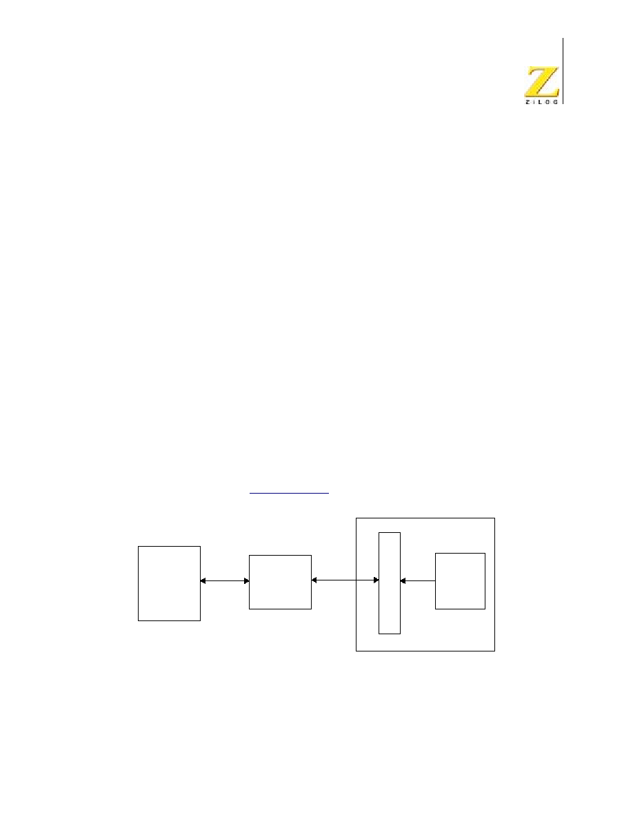
eZ80190 Product Specification
PS006611-0703
PRELIMINARY
ZiLOG Debug Interface
146
ZiLOG Debug Interface
ZDI Overview
The ZiLOG Debug Interface (ZDI) provides a built-in debugging interface to the
eZ80
Æ
CPU. ZDI provides basic in-circuit emulation features such as:
∑
Examining and modifying internal registers
∑
Examining and modifying memory
∑
Starting and stopping the user program
∑
Setting program and data break points
∑
Single-stepping the user program
∑
Executing user-supplied instructions
∑
Debugging the final product with the inclusion of one small connector
∑
Downloading code into SRAM
∑
C source-level debugging using ZiLOG Developer Studio
II (ZDS
II)
The above features are built into the silicon. Control is provided via a two-wire
interface that is connected to the ZPAK
II emulator. Figure 26 illustrates a typical
setup using a a target board, ZPAK
II, and the host PC running ZiLOG Developer
Studio. Refer to the
ZiLOG web site
for more information on ZPAK
II and ZDS
II.
The ZDI block for the eZ80190 device provides increased functionality from previ-
ous versions. ZDI allows reading and writing of most of the internal registers with-
out disturbing the state of the machine. New features allow READs and writes to
Figure 26. Typical ZDI Debug Setup
User's Target Board
C
o
n
n
e
c
t
o
r
ZPAK II
eZ80 190
Emulator
ZiLOG
Developer
Studio II
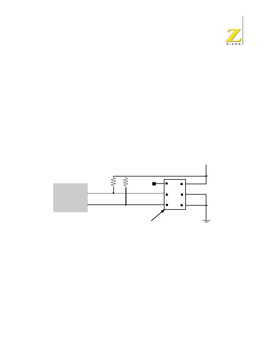
eZ80190 Product Specification
PS006611-0703
PRELIMINARY
ZiLOG Debug Interface
147
memory to occur as fast as the ZDI can download and upload data, with a maxi-
mum frequency of one-half the CPU clock frequency.
ZDI Interface
ZDI supports a bidirectional serial protocol. The protocol defines any device that
sends data as the transmitter and any receiving device as the receiver. The
device controlling the transfer is the master and the device being controlled is the
slave. The master always initiates the data transfers and provides the clock for
both receive and transmit operations. The ZDI block on the eZ80190 device is
considered a slave in all data transfers.
Figure 27 illustrates the schematic for building a connector on a target board. This
connector allows the user to connect directly to the ZPAK
II emulator using a six-
pin header.
ZDI Clock and Data Conventions
The two pins used for communication with the ZDI block are the ZDI Clock pin
(ZCL) and the ZDI Data pin (ZDA). For general data communication, the data
value on the ZDA pin can change only when ZCL is Low (0). The only exception is
the ZDI START bit, which is indicated by a High-to-Low transition (falling edge) on
the ZDA pin while ZCL is High.
Data is shifted into and out of ZDI, with the most significant bit (bit 7) of each byte
being transferred first, and the least significant bit (bit 0) transferred last. All infor-
mation is passed between the master and the slave in 8-bit (single-byte) units.
Each byte is transferred with nine clock cycles: eight to shift the data, and the
ninth for internal operations.
Figure 27. Schematic For Building a Target Board ZPAK
II Connector
TARGET
PROCESSOR
330K
330K
TV
DD
(Target V
DD
)
1
2
3
4
5
6
6-Pin Target Connector
ZDA
ZCL

eZ80190 Product Specification
PS006611-0703
PRELIMINARY
ZiLOG Debug Interface
148
ZDI START Condition
All ZDI commands are preceded by the ZDI START signal, which is a High-to-Low
transition of ZDA when ZCL is High. The ZDI slave on the eZ80190 device contin-
ually monitors the ZDA and ZCL lines for the START signal and does not respond
to any command until this condition is met. The master pulls ZDA Low, with ZCL
High, to indicate the beginning of a data transfer with the ZDI block. Figures 28
and 29 illustrate a valid ZDI START signal prior to writing and reading data,
respectively. A Low-to-High transition of ZDA while the ZCL is High produces no
effect.
Data is shifted in during a write to the ZDI block on the rising edge of ZCL, as illus-
trated in Figure 28. Data is shifted out during a read from the ZDI block on the fall-
ing edge of ZCL, as illustrated in Figure 29. When an operation is completed, the
master stops during the ninth cycle and holds the ZCL signal High.
Figure 28. ZDI Write Timing
Figure 29. ZDI Read Timing
ZCL
ZDA
ZDA
Change
ZDA
Change
ZDA
Change
ZDA
Stable
ZDA
Stable
Start Signal
ZDI Data In
(write)
ZDI Data In
(write)
ZCL
ZDA
ZDA
Change
ZDA
Change
ZDA
Change
ZDA
Stable
ZDA
Stable
Start Signal
ZDI Data Out
(read)
ZDI Data Out
(read)

eZ80190 Product Specification
PS006611-0703
PRELIMINARY
ZiLOG Debug Interface
149
ZDI Single-Bit Byte Separator
Following each 8-bit ZDI data transfer, a single-bit byte separator is used. The
ZDA pin should be forced High (1) prior to the ZCL rising edge for this 9
th
bit. For
most ZDI operations, the ZDI register address automatically increments during
this single-bit byte separator period. The same read or write operation as just
completed can then be immediately performed on the next ZDI register. If a differ-
ent operation or register address is required, a ZDI START signal during the byte
separator bit can be used to terminate the previous read or write operation and
signify initiation of a new ZDI register operation.
ZDI Register Addressing
Following a START signal, the ZDI master must output the ZDI register address.
All data transfers with the ZDI block use special ZDI registers. The ZDI control
registers that reside in the ZDI register address space should not be confused
with the eZ80190 device peripheral registers that reside in the I/O addressing
space of the eZ80190 device.
Many locations in the ZDI control register address space are shared by two regis-
ters, one for Read Only access and one for Write Only access. As an example, a
read from ZDI register address
00h
returns the Product ID Low Byte while a write
to this same location,
00h
, stores the Low byte of one of the address match values
used for generating break points.
The format for a ZDI address is seven bits of address, followed by one bit for read
or write control, and completed by a single-bit byte separator in which ZDA must
be 1. The data separator time period is used to allow the ZDI master to send a
new ZDI START signal, if necessary. The ZDI executes a read or write operation
depending on the state of the R/W bit (0 = write, 1 = read). Figure 30 illustrates
the timing for address writes to ZDI registers.
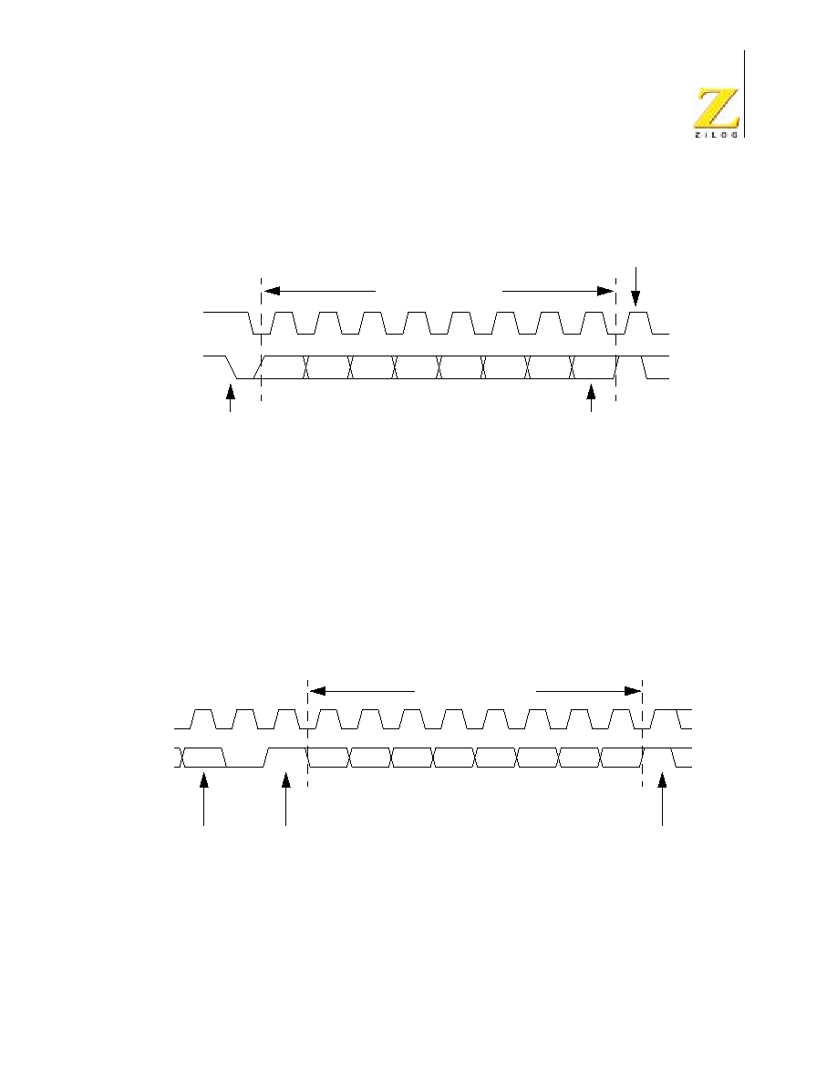
eZ80190 Product Specification
PS006611-0703
PRELIMINARY
ZiLOG Debug Interface
150
ZDI Write Operations
ZDI Single-Byte Write
For single-byte write operations, the address and write-control bit are first written
to the ZDI block. Following the 1-bit byte separator, the data is shifted into the ZDI
block on the next 8 rising edges of ZCL. The master terminates activity after 8
clock cycles. Figure 31 illustrates the timing for ZDI single-byte WRITE opera-
tions.
Figure 30. ZDI Address Write Timing
Figure 31. ZDI Single-Byte Data Write Timing
ZCL
ZDA
Start
Signal
A6
A5
A4
A3
A2
A1
A0
R/W
msb
lsb
ZDI Address Byte
0 = write
1 = read
S
1
2
3
4
5
6
7
8
9
1
Single-Bit
Byte Separator
or new ZDI
START Signal
ZCL
ZDA
A0
Write
1
D7
D6
D5
D4
D3
lsb of
msb
ZDI Data Byte
7
8
9
1
2
3
4
5
6
D2
7
8
9
D1
D0
1
ZDI
address
1-bit data
separator
of
DATA
lsb
of
DATA
end of data
or new ZDI
START signal
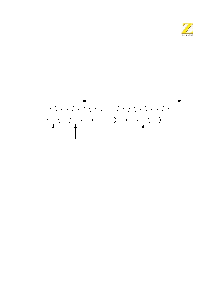
eZ80190 Product Specification
PS006611-0703
PRELIMINARY
ZiLOG Debug Interface
151
ZDI Block Write
The block WRITE operation is initiated in the same manner as the single-byte
write operation. After the first data byte is transferred, the ZDI master continues to
transmit additional bytes of data to the ZDI slave on the eZ80190 device. After the
receipt of each byte of data the ZDI register address increments by one. If the ZDI
register address reaches the end of the Write Only ZDI register address space
(
30h
), the address stops incrementing. Figure 32 illustrates the timing for ZDI
block WRITE operations.
ZDI Read Operations
ZDI Single-Byte READ
Single-byte read operations are initiated in the same manner as single-byte write
operations, with the exception that the R/W bit of the ZDI register address is set to
1. Upon receipt of a slave address with the R/W bit set to 1, the eZ80190 device's
ZDI block loads the selected data into the shifter at the beginning of the first cycle
following the 1-bit data separator. The most significant bit (msb) is shifted out first.
Figure 33 illustrates the timing for ZDI single-byte WRITE operations.
Figure 32. ZDI Block Data Write Timing
ZCL
ZDA
A0
1
D7
D6
D1
D0
lsb of
msb
ZDI Data Bytes
7
8
9
1
2
7
8
9
1
1
2
D7
D6
ZDI
address
1-bit data
separator
of
DATA
1-bit data
separator
lsb
of
DATA
byte 1
byte 1
msb
of
DATA
byte 2
Write

eZ80190 Product Specification
PS006611-0703
PRELIMINARY
ZiLOG Debug Interface
152
ZDI Block READ
A block READ operation is initiated the same as a single-byte read; however, the
ZDI master continues to clock in the next byte from the ZDI slave as the ZDI slave
continues to output data. The ZDI register address counter increments with each
read. If the ZDI register address reaches the end of the Read Only ZDI register
address space (
20h
), the address stops incrementing. Figure 34 illustrates ZDI
block READ timing.
Operation Of The eZ80190 Device During ZDI Breakpoints
If the ZDI forces the CPU to break, only the CPU suspends operation. The system
clock continues to operate and drive other peripherals. Those peripherals that can
operate autonomously from the CPU may continue to operate, if so enabled. For
Figure 33. ZDI Single-Byte Data Read Timing
Figure 34. ZDI Block Data Read Timing
ZCL
ZDA
A0
Read
1
D7
D6
D5
D4
D3
lsb of
msb
ZDI Data Byte
7
8
9
1
2
3
4
5
6
D2
7
8
9
D1
D0
1
ZDI
address
1-bit data
separator
of
DATA
lsb
of
DATA
End of data
or new ZDI
START signal
ZCL
ZDA
A0
1
D7
D6
D1
D0
lsb of
msb
ZDI Data Bytes
7
8
9
1
2
7
8
9
1
1
2
D7
D6
ZDI
address
1-bit data
separator
of
DATA
1-bit data
separator
lsb
of
DATA
byte 1
byte 1
msb
of
DATA
byte 2
Read

eZ80190 Product Specification
PS006611-0703
PRELIMINARY
ZiLOG Debug Interface
153
example, the Watch-Dog Timer and Programmable Reload Timers continue to
count during a ZDI breakpoint.
When using the ZDI interface, any write or read operations of peripheral registers
in the I/O address space produces the same effect as read or write operations
using the CPU. Because many register Read/Write operations exhibit secondary
effects, such as clearing flags or causing operations to commence, the effects of
the Read/Write operations during a ZDI break must be taken into consideration.
As an example, reading or writing the MACC Accumulator Byte 4 register can
cause a bank switch to occur within the MACC.
ZDI Write Only Registers
Table 81 lists the ZDI Write Only registers. Many of the ZDI Write Only addresses
are shared with ZDI Read Only registers.
Table 81. ZDI Write Only Registers
ZDI Address
ZDI Register Name
ZDI Register Function
Reset
Value
Page #
00h
ZDI_ADDR0_L
Address Match 0 Low Byte
XXh
155
01h
ZDI_ADDR0_H
Address Match 0 High Byte
XXh
02h
ZDI_ADDR0_U
Address Match 0 Upper Byte
XXh
04h
ZDI_ADDR1_L
Address Match 1 Low Byte
XXh
05h
ZDI_ADDR1_H
Address Match 1 High Byte
XXh
06h
ZDI_ADDR1_U
Address Match 1 Upper Byte
XXh
08h
ZDI_ADDR2_L
Address Match 2 Low Byte
XXh
09h
ZDI_ADDR2_H
Address Match 2 High Byte
XXh
0Ah
ZDI_ADDR2_U
Address Match 2 Upper Byte
XXh
0Ch
ZDI_ADDR3_L
Address Match 3 Low Byte
XXh
0Dh
ZDI_ADDR3_H
Address Match 3 High Byte
XXh
0Eh
ZDI_ADDR3_U
Address Match 4 Upper Byte
XXh
10h
ZDI_BRK_CTL
Break Control register
00h
156
13h
ZDI_WR_DATA_L
Write Data Low Byte
XXh
158
14h
ZDI_WR_DATA_H
Write Data High Byte
XXh
158
15h
ZDI_WR_DATA_U
Write Data Upper Byte
XXh
158
16h
ZDI_RW_CTL
Read/Write Control register
00h
159

eZ80190 Product Specification
PS006611-0703
PRELIMINARY
ZiLOG Debug Interface
154
ZDI Read Only Registers
Table 82 lists the ZDI Read Only registers. Many of the ZDI Read Only addresses
are shared with ZDI Write Only registers.
ZDI Register Definitions
ZDI Address Match Registers
The 4 sets of address match registers are used for setting the addresses for gen-
erating break points. When the accompanying BRK_ADDRx bit is set in the ZDI
Break Control register to enable the particular address match, the current
21h
ZDI_IS4
Instruction Store 4
XXh
161
22h
ZDI_IS3
Instruction Store 3
XXh
23h
ZDI_IS2
Instruction Store 2
XXh
24h
ZDI_IS1
Instruction Store 1
XXh
25h
ZDI_IS0
Instruction Store 0
XXh
30h
ZDI_WR_MEM
Write Memory register
XXh
162
Table 82. ZDI Read Only Registers
ZDI Address
ZDI Register Name
ZDI Register Function
Reset
Value
Page #
00h
ZDI_ID_L
eZ80
Æ
Product ID Low Byte register
05h
162
01h
ZDI_ID_H
eZ80
Æ
Product ID High Byte register
00h
163
02h
ZDI_ID_REV
eZ80
Æ
Product ID Revision register
XXh
163
03h
ZDI_STAT
Status register
00h
164
10h
ZDI_RD_L
Read Memory Address Low Byte
register
XXh
165
11h
ZDI_RD_H
Read Memory Address High Byte
register
XXh
165
12h
ZDI_RD_U
Read Memory Address Upper Byte
register
XXh
165
20h
ZDI_RD_MEM
Read Memory Data Value
XXh
165
Table 81. ZDI Write Only Registers (Continued)
ZDI Address
ZDI Register Name
ZDI Register Function
Reset
Value
Page #
eZ80190 Product Specification
PS006611-0703
PRELIMINARY
ZiLOG Debug Interface
155
eZ80190 device address is compared with the 3-byte address set,
{ZDI_ADDRx_U, ZDI_ADDRx_H, ZDI_ADDR_x_L}. If the CPU is operating in
ADL mode, the address is provided by ADDR[23:0]. If the CPU is operating in Z80
mode, the address is provided by {MBASE[7:0], ADDR[15:0]}. If a match is found,
ZDI issues a break to the eZ80190 device placing the processor in ZDI mode
pending further instructions from the ZDI interface block. If the address is not the
first op-code fetch, the ZDI break is executed at the end of the instruction in which
it is executed. There are four sets of address match registers. They can be used
in conjunction with each other to break on branching instructions.
Due to pipelining functions within the CPU, if the ZDI match address is
placed 1 or 2 bytes after completion of a repeating instruction (such as
LDIR), the break is issued following completion of only a single cycle of the
repeat. When execution is resumed, the repeating instruction completes
as required.
Table 83. ZDI Address Match Registers
(ZDI_ADDR0_L = 00h, ZDI_ADDR0_H = 01h, ZDI_ADDR0_U = 02h, ZDI_ADDR1_L = 04h,
ZDI_ADDR1_H = 05h, ZDI_ADDR1_U = 06h, ZDI_ADDR2_L = 08h, ZDI_ADDR2_H = 09h,
ZDI_ADDR2_U = 0Ah, ZDI_ADDR3_L = 0Ch, ZDI_ADDR3_H = 0Dh, ZDI_ADDR3_U = 0Eh)
Bit
7
6
5
4
3
2
1
0
Reset
X
X
X
X
X
X
X
X
CPU Access
W
W
W
W
W
W
W
W
Note: X = Undefined; R/W = Read/Write.
Bit
Position
Value
Description
[7:0]
ZDI_ADDRX_L,
ZDI_ADDRX_H,
or
ZDI_ADDRX_U
00h≠
FFh
The 4 sets of ZDI address match registers are used for
setting the addresses for generating break points. The 24-
bit addresses are returned by {ZDI_ADDRx_U,
ZDI_ADDRx_H, ZDI_ADDRx_L, where x is 0, 1, 2, or 3.
Note:

eZ80190 Product Specification
PS006611-0703
PRELIMINARY
ZiLOG Debug Interface
156
ZDI Break Control Register
The ZDI Break Control register, Table 84, is used to enable break points.
Table 84. ZDI Break Control Register
(ZDI_BRK_CTL = 10h in the ZDI Write Only Register Address Space)
Bit
7
6
5
4
3
2
1
0
Reset
0
0
0
0
0
0
0
0
CPU Access
W
W
W
W
W
W
W
W
Note: W = Write Only.
Bit
Position
Value
Description
7
BRK_NEXT
0
The ZDI break on the next CPU instruction is disabled.
1
The ZDI break on the next CPU instruction is enabled. The
CPU is instructed to use multiple Op Codes and multiple byte
operands. This function only breaks on the first Op Code in a
multiple Op Code instruction. If both the ZCL and ZDA pins
are forced Low (0) during a RESET, this bit is set to 1 and a
break occurs on the first instruction following the RESET.
6
BRK_ADDR3
0
The ZDI break, upon matching break address 3, is disabled.
1
The ZDI break, upon matching break address 3, is enabled.
ZDI asserts a break when the CPU address, ADDR[23:0],
matches the value in the ZDI Address Match 3 registers,
{ZDI_ADDR3_U, ZDI_ADDR3_H, ZDI_ADDR3_L}. Breaks
can only occur on an instruction boundary. If the address is
not the beginning of an instruction, then the break occurs at
the end of the current instruction. The break is implemented
by setting the BRK_NEXT bit to 1.The BRK_NEXT bit must be
reset to 0 to release the break.
5
BRK_ADDR2
0
The ZDI break, upon matching break address 2, is disabled.
1
The ZDI break, upon matching break address 2, is enabled.
ZDI asserts a break when the CPU address, ADDR[23:0],
matches the value in the ZDI Address Match 2 registers,
{ZDI_ADDR2_U, ZDI_ADDR2_H, ZDI_ADDR2_L}. Breaks
can only occur on an instruction boundary. If the address is
not the beginning of an instruction, then the break occurs at
the end of the current instruction. The break is implemented
by setting the BRK_NEXT bit to 1. The BRK_NEXT bit must
be reset to 0 to release the break.

eZ80190 Product Specification
PS006611-0703
PRELIMINARY
ZiLOG Debug Interface
157
4
BRK_ADDR1
0
The ZDI break, upon matching break address 1, is disabled.
1
The ZDI break, upon matching break address 1, is enabled.
ZDI asserts a break when the CPU address, ADDR[23:0],
matches the value in the ZDI Address Match 1 registers,
{ZDI_ADDR1_U, ZDI_ADDR1_H, ZDI_ADDR1_L}. If the
IGN_LOW_1 bit is set to 1, ZDI asserts a break with the upper
two bytes of the CPU address, ADDR[23:8], and matches the
value in the ZDI Address Match 1 High and Low Byte
registers, {ZDI_ADDR1_U, ZDI_ADDR1_LH}. The lower byte
of the address is ignored. Breaks can only occur on an
instruction boundary. If the address is not the beginning of an
instruction, then the break occurs at the end of the current
instruction. The break is implemented by setting the
BRK_NEXT bit to 1. The BRK_NEXT bit must be reset to 0 to
release the break.
4
BRK_ADDR0
0
The ZDI break, upon matching break address 0, is disabled.
1
The ZDI break, upon matching break address 0, is enabled.
ZDI asserts a break when the CPU address, ADDR[23:0],
matches the value in the ZDI Address Match 1 registers,
{ZDI_ADDR0_U, ZDI_ADDR0_H, ZDI_ADDR0_L}. If the
IGN_LOW_0 bit is set to 1, ZDI asserts a break with the upper
two bytes of the CPU address, ADDR[23:8], and matches the
value in the ZDI Address Match 0 High and Low Byte
registers, {ZDI_ADDR0_U, ZDI_ADDR0_LH}. The lower byte
of the address is ignored. Breaks can only occur on an
instruction boundary. If the address is not the beginning of an
instruction, then the break occurs at the end of the current
instruction.The break is implemented by setting the
BRK_NEXT bit to 1. The BRK_NEXT bit must be reset to 0 to
release the break.
2
IGN_LOW_1
0
The Ignore the Low byte function of the ZDI Address Match 1
registers is disabled. If BRK_ADDR1 is set to 1, ZDI initiates a
break when the entire 24-bit address, ADDR[23:0], matches
the 3-byte value {ZDI_ADDR1_U, ZDI_ADDR1_H,
ZDI_ADDR1_L}.
1
The Ignore the Low byte function of the ZDI Address Match 1
registers is enabled. If BRK_ADDR1 is set to 1, ZDI initiates a
break when only the upper 2 bytes of the 24-bit address,
ADDR[23:8], match the 2-byte value {ZDI_ADDR1_U,
ZDI_ADDR1_H}. As a result, a break can occur anywhere
within a 256-byte page.
Bit
Position
Value
Description

eZ80190 Product Specification
PS006611-0703
PRELIMINARY
ZiLOG Debug Interface
158
ZDI Write Data Registers
Three registers are used in the ZDI Write Only register address space to store the
data that is written when a write instruction is sent to the ZDI Read/Write Control
register (ZDI_RW_CTL). The ZDI Read/Write Control register, indicated in
Table 86, is located at ZDI address
16h
immediately following the ZDI Write Data
registers, in Table 85. As a result, the ZDI master is allowed to write the data to
{ZDI_WR_U, ZDI_WR_H, ZDI_WR_L} and the write command in one data trans-
fer operation.
1
IGN_LOW_0
0
The Ignore the Low byte function of the ZDI Address Match 1
registers is disabled. If BRK_ADDR0 is set to 1, ZDI initiates a
break when the entire 24-bit address, ADDR[23:0], matches
the 3-byte value {ZDI_ADDR0_U, ZDI_ADDR0_H,
ZDI_ADDR0_L}.
1
The Ignore the Low byte function of the ZDI Address Match 1
registers is enabled. If the BRK_ADDR1 is set to 0, ZDI
initiates a break when only the upper 2 bytes of the 24-bit
address, ADDR[23:8], match the 2 bytes value
{ZDI_ADDR0_U, ZDI_ADDR0_H}. As a result, a break can
occur anywhere within a 256-byte page.
0
SINGLE_STEP
0
ZDI SINGLE STEP mode is disabled.
1
ZDI SINGLE STEP mode is enabled. ZDI asserts a break
following execution of each instruction.
Table 85. ZDI Write Data Registers
(ZDI_WR_U = 13h, ZDI_WR_H = 14h, ZDI_WR_L = 15h)
Bit
7
6
5
4
3
2
1
0
Reset
X
X
X
X
X
X
X
X
CPU Access
W
W
W
W
W
W
W
W
Note: X = Undefined; W = Write.
Bit
Position
Value
Description
[7:0]
ZDI_WR_L,
ZDI_WR_H,
or
ZDI_WR_L
00h≠
FFh
These registers contain the data that is written during
execution of a write operation defined by the
ZDI_RW_CTL register. The 24-bit data value is stored as
{ZDI_WR_U, ZDI_WR_H, ZDI_WR_L}. If less than 24 bits
of data are required to complete the required operation,
the data is taken from the least significant byte(s).
Bit
Position
Value
Description

eZ80190 Product Specification
PS006611-0703
PRELIMINARY
ZiLOG Debug Interface
159
ZDI Read/Write Control Register
The ZDI Read/Write Control register is used in the ZDI Write Only Register
address to read data from, write data to, and manipulate the CPU's registers or
memory locations. When this register is written, the eZ80190 device immediately
performs the operation corresponding to the data value written as described in
Table 86. When a read operation is executed via this register, the requested data
values are placed in the ZDI Read Data registers {ZDI_RD_U, ZDI_RD_H,
ZDI_RD_L}. When a write operation is executed via this register, the write data is
taken from the ZDI Write Data registers {ZDI_WR_U, ZDI_WR_H, ZDI_WR_L}.
Refer to the
eZ80 CPU User Manual
for information regarding the CPU registers.
Table 86. ZDI Read/Write Control Register Functions
(ZDI_RW_CTL = 16h)
Hex
Value
Command
Hex
Value
Command
00
Read {MBASE, A, F}
ZDI_RD_U
MBASE
ZDI_RD_H
F
ZDI_RD_L
A
80
Write AF
MBASE
ZDI_WR_U
F
ZDI_WR_H
A
ZDI_WR_L
01
Read BC
ZDI_RD_U
BCU
ZDI_RD_H
B
ZDI_RD_L
C
81
Write BC
BCU
ZDI_WR_U
B
ZDI_WR_H
C
ZDI_WR_L
02
Read DE
ZDI_RD_U
DEU
ZDI_RD_H
D
ZDI_RD_L
E
82
Write DE
DEU
ZDI_WR_U
D
ZDI_WR_H
E
ZDI_WR_L
03
Read HL
ZDI_RD_U
HLU
ZDI_RD_H
H
ZDI_RD_L
L
83
Write HL
HLU
ZDI_WR_U
H
ZDI_WR_H
L
ZDI_WR_L
04
Read IX
ZDI_RD_U
IXU
ZDI_RD_H
IXH
ZDI_RD_L
IXL
84
Write IX
IXU
ZDI_WR_U
IXH
ZDI_WR_H
IXL
ZDI_WR_L
05
Read IY
ZDI_RD_U
IYU
ZDI_RD_H
IYH
ZDI_RD_L
IYL
85
Write IY
IYU
ZDI_WR_U
IYH
ZDI_WR_H
IYL
ZDI_WR_L
Note: The CPU's alternate register set (A', F', B', C', D', E', HL') cannot be read directly. The ZDI
programmer must execute the exchange instruction (EXX) to gain access to the alternate
CPU register set.

eZ80190 Product Specification
PS006611-0703
PRELIMINARY
ZiLOG Debug Interface
160
Instruction Store 4:0 Registers
The ZDI Instruction Store registers, indicated in Table 87, are located in the ZDI
Register Write Only address space. They can be written with instruction data for
direct execution by the CPU. When the ZDI_IS0 register is written, the eZ80190
device exits the ZDI BREAK mode and executes a single instruction. The Op
Codes and operands for the instruction are received from these Instruction Store
registers. Instruction Store Register 0 is the first byte fetched, followed by Instruc-
tion Store registers 1, 2, 3 and 4, as necessary. Only the bytes the processor
requires to execute the instruction must be stored in these registers. Some eZ80
Æ
CPU instructions, when combined with the MEMORY mode suffixes (.SIS, .SIL,
.LIS, or .LIL), require 6 bytes to operate. These 6-byte instructions cannot be exe-
cuted directly using the ZDI Instruction Store registers.
The Instruction Store 0 register resides at a higher ZDI address than the
other Instruction Store registers. This feature allows the use of the ZDI
06
Read SP
In ADL mode, SP = SPL.
In Z80 mode, SP = SPS.
86
Write SP
In ADL mode, SP = SPL.
In Z80 mode, SP = SPS.
07
Read PC
ZDI_RD_U
PC[23:16]
ZDI_RD_H
PC[15:8]
ZDI_RD_L
PC[7:0]
87
Write PC
PC[23:16]
ZDI_WR_U
PC[15:8]
ZDI_WR_H
PC[7:0]
ZDI_WR_L
08
Set ADL
ADL
1
88
Reserved
09
Reset ADL
ADL
0
89
Reserved
0A
Exchange CPU register sets
AF
AF'
BC
BC'
DE
DE'
HL
HL'
8A
Reserved
0B
Read memory from current
PC value, increment PC
8B
Write memory from current PC
value, increment PC
Table 86. ZDI Read/Write Control Register Functions
(ZDI_RW_CTL = 16h) (Continued)
Hex
Value
Command
Hex
Value
Command
Note: The CPU's alternate register set (A', F', B', C', D', E', HL') cannot be read directly. The ZDI
programmer must execute the exchange instruction (EXX) to gain access to the alternate
CPU register set.
Note:
eZ80190 Product Specification
PS006611-0703
PRELIMINARY
ZiLOG Debug Interface
161
auto-address increment function to load up and execute an instruction with
a single data stream from the ZDI master.
ZDI Write Memory Register
A write to the ZDI Write Memory register, indicated in Table 88, causes the
eZ80190 device to write the 8-bit data to the memory location specified by the cur-
rent address in the program counter. In Z80 MEMORY mode, this address is
{MBASE, PC[15:0]}. In ADL MEMORY mode, this address is PC[23:0]. The pro-
gram counter, PC, increments after each data write. However, the ZDI register
address does not increment automatically when this register is accessed. As a
result, the ZDI master is allowed to write any number of data bytes by writing to
this address one time, and then writing any number of data bytes.
Table 87. Instruction Store 4:0 Registers
(ZDI_IS4 = 21h, ZDI_IS3 = 22h, ZDI_IS2 = 23h, ZDI_IS1 = 24h, ZDI_IS0 = 25h)
Bit
7
6
5
4
3
2
1
0
Reset
X
X
X
X
X
X
X
X
CPU Access
W
W
W
W
W
W
W
W
Note: X = Undefined; W = Write.
Bit
Position
Value
Description
[7:0]
ZDI_IS4,
ZDI_IS3,
ZDI_IS2,
ZDI_IS1,
or ZDI_IS0
00h≠
FFh
These registers contain the Op Codes and operands for
immediate execution by the CPU following a write to
ZDI_IS0. The ZDI_IS0 register contains the first Op Code
of the instruction. The remaining ZDI_ISx registers
contain any additional Op Codes or operand dates
required for execution of the required instruction.
eZ80190 Product Specification
PS006611-0703
PRELIMINARY
ZiLOG Debug Interface
162
eZ80
Æ
Product ID Low Byte Register
The Product ID Low and High Byte registers, indicated in Table 89, combine to
provide a means for an external device to determine the particular Product prod-
uct being addressed. For the eZ80190 device, these two bytes {ZDI_ID_H,
ZDI_ID_L}, return the value {
00h
,
05h
}.
eZ80
Æ
Product ID High Byte Register
The Product ID Low and High Byte registers, indicated in Table 90, combine to
provide a means for an external device to determine the particular Product prod-
uct being addressed. For the eZ80190 device, these two bytes {ZDI_ID_H,
ZDI_ID_L}, return the value {
00h
,
05h
}.
Table 88. ZDI Write Memory Register
(ZDI_WR_MEM = 30h in the ZDI Register Write Only Address Space)
Bit
7
6
5
4
3
2
1
0
Reset
X
X
X
X
X
X
X
X
CPU Access
W
W
W
W
W
W
W
W
Note: X = Undefined; W = Write.
Bit
Position
Value
Description
[7:0]
ZDI_WR_MEM
00h≠
FFh
The 8-bit data that is transferred to the ZDI slave following a
write to this address is written to the address indicated by the
current program counter. The program counter is incremented
following each 8-bits of data. In Z80 MEMORY mode, ({MBASE,
PC[15:0]})
8 bits of transferred data. In ADL MEMORY mode,
(PC[23:0])
8-bits of transferred data.
Table 89. eZ80
Æ
Product ID Low Byte Register
(ZDI_ID_L = 00h in ZDI Register Read Only Address Space)
Bit
7
6
5
4
3
2
1
0
Reset
0
0
0
0
0
1
0
1
CPU Access
R
R
R
R
R
R
R
R
Note: R = Read Only.
Bit
Position
Value
Description
[7:0]
ZDI_ID_L
05h
{ZDI_ID_H, ZDI_ID_L} = {00h, 05h} indicates the
eZ80190 product.

eZ80190 Product Specification
PS006611-0703
PRELIMINARY
ZiLOG Debug Interface
163
eZ80
Æ
Product ID Revision Register
The Product ID Revision register, indicated in Table 91, identifies the current revi-
sion of the eZ80190 product. This number is changed for each revision.
Table 90. eZ80
Æ
Product ID High Byte Register
(ZDI_ID_H = 01h in the ZDI Register Read Only Address Space)
Bit
7
6
5
4
3
2
1
0
Reset
0
0
0
0
0
1
0
0
CPU Access
R
R
R
R
R
R
R
R
Note: R = Read Only.
Bit
Position
Value
Description
[7:0]
ZDI_ID_H
00h
{ZDI_ID_H, ZDI_ID_L} = {00h, 05h} indicates the
eZ80190
product.
Table 91. eZ80
Æ
Product ID Revision Register
(ZDI_ID_REV = 02h in the ZDI Register Read Only Address Space)
Bit
7
6
5
4
3
2
1
0
Reset
X
X
X
X
X
X
X
X
CPU Access
R
R
R
R
R
R
R
R
Note: X = Undetermined; R = Read Only.
Bit
Position
Value
Description
[7:0]
ZDI_ID_REV
00h≠
FFh
Identifies the current revision of the eZ80190 product.

eZ80190 Product Specification
PS006611-0703
PRELIMINARY
ZiLOG Debug Interface
164
ZDI Status Register
The ZDI Status register, indicated in Table 92, provides current information on the
eZ80190 device and the CPU.
ZDI Read Register Low, High, and Upper
The ZDI register Read Only address space offers Low, High, and Upper functions,
which contain the value read by a read operation from the ZDI Read/Write Control
register (ZDI_RW_CTL). This data is valid only while in ZDI BREAK mode and
only if the instruction is read by a request from the ZDI Read/Write Control regis-
ter. See Table 93.
Table 92. ZDI Status Register
(ZDI_STAT = 03h in the ZDI Register Read Only Address Space)
Bit
7
6
5
4
3
2
1
0
Reset
0
0
0
0
0
0
0
0
CPU Access
R
R
R
R
R
R
R
R
Note: R = Read Only.
Bit
Position
Value
Description
7
ZDI_ACTIVE
0
The CPU is not functioning in ZDI mode.
1
The CPU is currently functioning in ZDI mode.
6
RESET_PEND
0
No RESET event is currently in progress.
1
A RESET event is in progress.
5
HALT
0
eZ80190 is not currently in HALT mode.
1
eZ80190 is currently in HALT mode.
4
ADL
0
The CPU is operating in Z80 MEMORY mode (ADL bit
flag = 0).
1
The CPU is operating in ADL MEMORY mode (ADL bit
flag = 1).
3
MADL
0
The CPU's Mixed-Memory mode (MADL) bit is reset to 0.
1
The CPU's Mixed-Memory mode (MADL) bit is set to 1.
2
IEF1
0
The CPU's Interrupt Enable Flag 1 is reset to 0. Maskable
interrupts are disabled.
1
The CPU's Interrupt Enable Flag 1 is set to 1. Maskable
interrupts are enabled.
[1:0]
00b
Reserved--must be 0.
eZ80190 Product Specification
PS006611-0703
PRELIMINARY
ZiLOG Debug Interface
165
ZDI Read Memory Data Value Register
When a read is executed from the ZDI Read Memory Data Value register, indi-
cated in Table 94, the eZ80190 device fetches the data from the memory address
currently pointed to by the program counter, PC, and the program counter is incre-
mented. In Z80 mode, the memory address is {MBASE, PC[15:0]}. In ADL mode,
the memory address is PC[23:0]. Refer to the
eZ80 CPU User Manual
for more
information regarding Z80 and ADL MEMORY modes. The program counter, PC,
increments after each data read. However, the ZDI register address does not
increment automatically when this register is accessed. As a result, the ZDI mas-
ter can read any number of data bytes from this address one time, then continue
to any number of 8-bit data bytes.
Table 93. ZDI Read Registers--Low, High and Upper
(ZDI_RD_L = 10h, ZDI_RD_H = 11h, ZDI_RD_U = 12h)
Bit
7
6
5
4
3
2
1
0
Reset
0
0
0
0
0
0
0
0
CPU Access
R
R
R
R
R
R
R
R
Note: R = Read Only.
Bit
Position
Value
Description
[7:0]
ZDI_RD_L,
ZDI_RD_H,
or
ZDI_RD_U
00h≠
FFh
Values read from the memory location as requested by
the ZDI Read Control register during a ZDI read
operation. The 24-bit value is stored in {ZDI_RD_U,
ZDI_RD_H, ZDI_RD_L}.
Table 94. ZDI Read Memory Data Value Register
(ZDI_RD_MEM = 20h in ZDI Register Read Only Address Space)
Bit
7
6
5
4
3
2
1
0
Reset
0
0
0
0
0
0
0
0
CPU Access
R
R
R
R
R
R
R
R
Note: R = Read Only.
Bit
Position
Value
Description
[7:0]
ZDI_RD_MEM
00h≠
FFh
8-bit data read from the memory address indicated by the
CPU's program counter. In Z80 mode, 8-bit data
transferred out
({MBASE, SPS}). In ADL mode, 8-bit
data transferred out
(SPL).

eZ80190 Product Specification
PS006611-0703
PRELIMINARY
eZ80
Æ
CPU Instruction Set
166
eZ80
Æ
CPU Instruction Set
Tables 95 through 104 indicate the eZ80
Æ
CPU instructions available for use with
the eZ80190 device. The instructions are grouped by class. More detailed infor-
mation is available in the
eZ80 CPU User Manual
.
The Sleep (SLP) instruction is not supported on the eZ80190 device. Exe-
cuting a SLP instruction causes the eZ80190 device to behave as if it has
received a two-cycle NOP instruction.
Table 95. Arithmetic Instructions
Mnemonic
Instruction
ADC
Add with Carry
ADD
Add without Carry
CP
Compare with Accumulator
DAA
Decimal Adjust Accumulator
DEC
Decrement
INC
Increment
MLT
Multiply
NEG
Negate Accumulator
SBC
Subtract with Carry
SUB
Subtract without Carry
Table 96. Bit Manipulation Instructions
Mnemonic
Instruction
BIT
Bit Test
RES
Reset Bit
SET
Set Bit
Table 97. Block Transfer and Compare Instructions
Mnemonic
Instruction
CPD (CPDR)
Compare and Decrement (with Repeat)
CPI (CPIR)
Compare and Increment (with Repeat)
LDD (LDDR)
Load and Decrement (with Repeat)
LDI (LDIR)
Load and Increment (with Repeat)
Note:

eZ80190 Product Specification
PS006611-0703
PRELIMINARY
eZ80
Æ
CPU Instruction Set
167
Table 98. Exchange Instructions
Mnemonic
Instruction
EX
Exchange registers
EXX
Exchange CPU Multibyte register banks
Table 99. Input/Output Instructions
Mnemonic
Instruction
IN
Input from I/O
IN0
Input from I/O on Page 0
IND (INDR)
Input from I/O and Decrement (with Repeat)
IND2 (IND2R)
Input from I/O and Decrement (with Repeat)
INDM (INDMR)
Input from I/O and Decrement (with Repeat)
INI (INIR)
Input from I/O and Increment (with Repeat)
INI2 (INI2R)
Input from I/O and Increment (with Repeat)
INIM (INIMR)
Input from I/O and Increment (with Repeat)
OTDM (OTDMR)
Output to I/O and Decrement (with Repeat)
OTIM (OTIMR)
Output to I/O and Increment (with Repeat)
OUT
Output to I/O
OUT0
Output to I/0 on Page 0
OUTD (OTDR)
Output to I/O and Decrement (with Repeat)
OUTD2 (OTD2R)
Output to I/O and Decrement (with Repeat)
OUTI (OTIR)
Output to I/O and Increment (with Repeat)
OUTI2 (OTI2R)
Output to I/O and Increment (with Repeat)
TSTIO
Test I/O
Table 100. Load Instructions
Mnemonic
Instruction
LD
Load
LEA
Load Effective Address
PEA
Push Effective Address
POP
Pop
PUSH
Push

eZ80190 Product Specification
PS006611-0703
PRELIMINARY
eZ80
Æ
CPU Instruction Set
168
Table 101. Logical Instructions
Mnemonic
Instruction
AND
Logical AND
CPL
Complement Accumulator
OR
Logical OR
TST
Test Accumulator
XOR
Logical Exclusive OR
Table 102. Processor Control Instructions
Mnemonic
Instruction
CCF
Complement Carry Flag
DI
Disable Interrupts
EI
Enable Interrupts
HALT
Halt
IM
Interrupt Mode
NOP
No Operation
RSMIX
Reset Mixed-Memory Mode Flag
SCF
Set Carry Flag
SLP
Sleep (not supported on the eZ80190 device)
STMIX
Set Mixed-Memory Mode Flag
Table 103. Program Control Instructions
Mnemonic
Instruction
CALL
Call Subroutine
CALL cc
Conditional Call Subroutine
DJNZ
Decrement and Jump if Nonzero
JP
Jump
JP cc
Conditional Jump
JR
Jump Relative
JR cc
Conditional Jump Relative
RET
Return
RET cc
Conditional Return
RETI
Return from Interrupt
RETN
Return from Nonmaskable interrupt
RST
Restart

eZ80190 Product Specification
PS006611-0703
PRELIMINARY
eZ80
Æ
CPU Instruction Set
169
Table 104. Rotate and Shift Instructions
Mnemonic
Instruction
RL
Rotate Left
RLA
Rotate Left≠Accumulator
RLC
Rotate Left Circular
RLCA
Rotate Left Circular≠Accumulator
RLD
Rotate Left Decimal
RR
Rotate Right
RRA
Rotate Right≠Accumulator
RRC
Rotate Right Circular
RRCA
Rotate Right Circular≠Accumulator
RRD
Rotate Right Decimal
SLA
Shift Left
SRA
Shift Right Arithmetic
SRL
Shift Right Logical
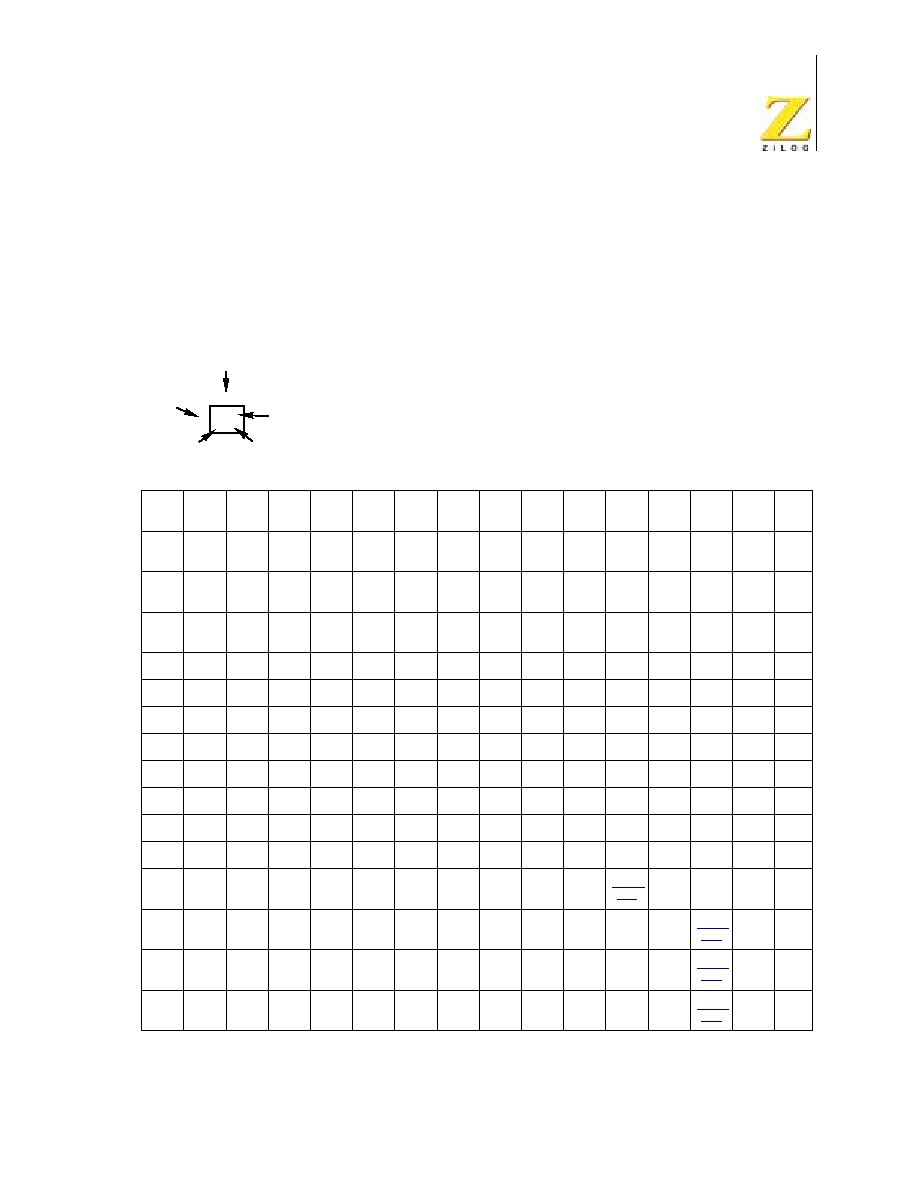
eZ80190 Product Specification
PS006611-0703
PRELIMINARY
Op-Code Map
170
Op-Code Map
Tables 105 through 111 indicate the hex values for each of the eZ80
Æ
instructions.
Table 105. Op Code Map--First Op Code
Lower Nibble (Hex)
0
1
2
3
4
5
6
7
8
9
A
B
C
D
E
F
Upper Nibble (Hex)
0
NOP
LD
BC,
Mmn
LD
(BC),A
INC
BC
INC
B
DEC
B
LD
B,n
RLCA
EX
AF,AF'
ADD
HL,BC
LD
A,(BC)
DEC
BC
INC
C
DEC
C
LD
C,n
RRCA
1
DJNZ
d
LD
DE,
Mmn
LD
(DE),A
INC
DE
INC
D
DEC
D
LD
D,n
RLA
JR
d
ADD
HL,DE
LD
A,(DE)
DEC
DE
INC
E
DEC
E
LD
E,n
RRA
2
JR
NZ,d
LD
HL,
Mmn
LD
(Mmn),
HL
INC
HL
INC
H
DEC
H
LD
H,n
DAA
JR
Z,d
ADD
HL,HL
LD
HL,
(Mmn)
DEC
HL
INC
L
DEC
L
LD
L,n
CPL
3
JR
NC,d
LD
SP,
Mmn
LD
(Mmn),
A
INC
SP
INC
(HL)
DEC
(HL)
LD
(HL),n
SCF
JR
CF,d
ADD
HL,SP
LD
A,
(Mmn)
DEC
SP
INC
A
DEC
A
LD
A,n
CCF
4
.SIS
suffix
LD
B,C
LD
B,D
LD
B,E
LD
B,H
LD
B,L
LD
B,(HL)
LD
B,A
LD
C,B
.LIS
suffix
LD
C,D
LD
C,E
LD
C,H
LD
C,L
LD
C,(HL)
LD
C,A
5
LD
D,B
LD
D,C
.SIL
suffix
LD
D,E
LD
D,H
LD
D,L
LD
D,(HL)
LD
D,A
LD
E,B
LD
E,C
LD
E,D
.LIL
suffix
LD
E,H
LD
E,L
LD
E,(HL)
LD
E,A
6
LD
H,B
LD
H,C
LD
H,D
LD
H,E
LD
H,H
LD
H,L
LD
H,(HL)
LD
H,A
LD
L,B
LD
L,C
LD
L,D
LD
L,E
LD
L,H
LD
L,L
LD
L,(HL)
LD
L,A
7
LD
(HL),B
LD
(HL),C
LD
(HL),D
LD
(HL),E
LD
(HL),H
LD
(HL),L
HALT
LD
(HL),A
LD
A,B
LD
A,C
LD
A,D
LD
A,E
LD
A,H
LD
A,L
LD
A,(HL)
LD
A,A
8
ADD
A,B
ADD
A,C
ADD
A,D
ADD
A,E
ADD
A,H
ADD
A,L
ADD
A,(HL)
ADD
A,A
ADC
A,B
ADC
A,C
ADC
A,D
ADC
A,E
ADC
A,H
ADC
A,L
ADC
A,(HL)
ADC
A,A
9
SUB
A,B
SUB
A,C
SUB
A,D
SUB
A,E
SUB
A,H
SUB
A,L
SUB
A,(HL)
SUB
A,A
SBC
A,B
SBC
A,C
SBC
A,D
SBC
A,E
SBC
A,H
SBC
A,L
SBC
A,(HL)
SBC
A,A
A
AND
A,B
AND
A,C
AND
A,D
AND
A,E
AND
A,H
AND
A,L
AND
A,(HL)
AND
A,A
XOR
A,B
XOR
A,C
XOR
A,D
XOR
A,E
XOR
A,H
XOR
A,L
XOR
A,(HL)
XOR
A,A
B
OR
A,B
OR
A,C
OR
A,D
OR
A,E
OR
A,H
OR
A,L
OR
A,(HL)
OR
A,A
CP
A,B
CP
A,C
CP
A,D
CP
A,E
CP
A,H
CP
A,L
CP
A,(HL)
CP
A,A
C
RET
NZ
POP
BC
JP
NZ,
Mmn
JP
Mmn
CALL
NZ,
Mmn
PUSH
BC
ADD
A,n
RST
00h
RET
Z
RET
JP
Z,
Mmn
Table
106
CALL
Z,
Mmn
CALL
Mmn
ADC
A,n
RST
08h
D
RET
NC
POP
DE
JP
NC,
Mmn
OUT
(n),A
CALL
NC,
Mmn
PUSH
DE
SUB
A,n
RST
10h
RET
CF
EXX
JP
CF,
Mmn
IN
A,(n)
CALL
CF,
Mmn
Table
107
SBC
A,n
RST
18h
E
RET
PO
POP
HL
JP
PO,
Mmn
EX
(SP),H
L
CALL
PO,
Mmn
PUSH
HL
AND
A,n
RST
20h
RET
PE
JP
(HL)
JP
PE,
Mmn
EX
DE,HL
CALL
PE,
Mmn
Table
108
XOR
A,n
RST
28h
F
RET
P
POP
AF
JP
P,
Mmn
DI
CALL
P,
Mmn
PUSH
AF
OR
A,n
RST
30h
RET
M
LD
SP,HL
JP
M,
Mmn
EI
CALL
M,
Mmn
Table
109
CP
A,n
RST
38h
Notes: n
=
8-bit data; Mmn
=
16- or 24-bit addr or data; d
=
8-bit two's-complement displacement.
AND
4
A
Lower Op Code Nibble
Mnemonic
Second Operand
Upper
Op Code
Nibble
First Operand
A,H
Legend

eZ80190 Product Specification
PS006611-0703
PRELIMINARY
Op-Code Map
171
Table 106. Op Code Map--Second Op Code after 0CBh
Lower Nibble (Hex)
0
1
2
3
4
5
6
7
8
9
A
B
C
D
E
F
Upper Nibble (Hex)
0
RLC
B
RLC
C
RLC
D
RLC
E
RLC
H
RLC
L
RLC
(HL)
RLC
A
RRC
B
RRC
C
RRC
D
RRC
E
RRC
H
RRC
L
RRC
(HL)
RRC
A
1
RL
B
RL
C
RL
D
RL
E
RL
H
RL
L
RL
(HL)
RL
A
RR
B
RR
C
RR
D
RR
E
RR
H
RR
L
RR
(HL)
RR
A
2
SLA
B
SLA
C
SLA
D
SLA
E
SLA
H
SLA
L
SLA
(HL)
SLA
A
SRA
B
SRA
C
SRA
D
SRA
E
SRA
H
SRA
L
SRA
(HL)
SRA
A
3
SRL
B
SRL
C
SRL
D
SRL
E
SRL
H
SRL
L
SRL
(HL)
SRL
A
4
BIT
0,B
BIT
0,C
BIT
0,D
BIT
0,E
BIT
0,H
BIT
0,L
BIT
0,(HL)
BIT
0,A
BIT
1,B
BIT
1,C
BIT
1,D
BIT
1,E
BIT
1,H
BIT
1,L
BIT
1,(HL)
BIT
1,A
5
BIT
2,B
BIT
2,C
BIT
2,D
BIT
2,E
BIT
2,H
BIT
2,L
BIT
2,(HL)
BIT
2,A
BIT
3,B
BIT
3,C
BIT
3,D
BIT
3,E
BIT
3,H
BIT
3,L
BIT
3,(HL)
BIT
3,A
6
BIT
4,B
BIT
4,C
BIT
4,D
BIT
4,E
BIT
4,H
BIT
4,L
BIT
4,(HL)
BIT
4,A
BIT
5,B
BIT
5,C
BIT
5,D
BIT
5,E
BIT
5,H
BIT
5,L
BIT
5,(HL)
BIT
5,A
7
BIT
6,B
BIT
6,C
BIT
6,D
BIT
6,E
BIT
6,H
BIT
6,L
BIT
6,(HL)
BIT
6,A
BIT
7,B
BIT
7,C
BIT
7,D
BIT
7,E
BIT
7,H
BIT
7,L
BIT
7,(HL)
BIT
7,A
8
RES
0,B
RES
0,C
RES
0,D
RES
0,E
RES
0,H
RES
0,L
RES
0,(HL)
RES
0,A
RES
1,B
RES
1,C
RES
1,D
RES
1,E
RES
1,H
RES
1,L
RES
1,(HL)
RES
1,A
9
RES
2,B
RES
2,C
RES
2,D
RES
2,E
RES
2,H
RES
2,L
RES
2,(HL)
RES
2,A
RES
3,B
RES
3,C
RES
3,D
RES
3,E
RES
3,H
RES
3,L
RES
3,(HL)
RES
3,A
A
RES
4,B
RES
4,C
RES
4,D
RES
4,E
RES
4,H
RES
4,L
RES
4,(HL)
RES
4,A
RES
5,B
RES
5,C
RES
5,D
RES
5,E
RES
5,H
RES
5,L
RES
5,(HL)
RES
5,A
B
RES
6,B
RES
6,C
RES
6,D
RES
6,E
RES
6,H
RES
6,L
RES
6,(HL)
RES
6,A
RES
7,B
RES
7,C
RES
7,D
RES
7,E
RES
7,H
RES
7,L
RES
7,(HL)
RES
7,A
C
SET
0,B
SET
0,C
SET
0,D
SET
0,E
SET
0,H
SET
0,L
SET
0,(HL)
SET
0,A
SET
1,B
SET
1,C
SET
1,D
SET
1,E
SET
1,H
SET
1,L
SET
1,(HL)
SET
1,A
D
SET
2,B
SET
2,C
SET
2,D
SET
2,E
SET
2,H
SET
2,L
SET
2,(HL)
SET
2,A
SET
3,B
SET
3,C
SET
3,D
SET
3,E
SET
3,H
SET
3,L
SET
3,(HL)
SET
3,A
E
SET
4,B
SET
4,C
SET
4,D
SET
4,E
SET
4,H
SET
4,L
SET
4,(HL)
SET
4,A
SET
5,B
SET
5,C
SET
5,D
SET
5,E
SET
5,H
SET
5,L
SET
5,(HL)
SET
5,A
F
SET
6,B
SET
6,C
SET
6,D
SET
6,E
SET
6,H
SET
6,L
SET
6,(HL)
SET
6,A
SET
7,B
SET
7,C
SET
7,D
SET
7,E
SET
7,H
SET
7,L
SET
7,(HL)
SET
7,A
Notes: n
=
8-bit data; Mmn
=
16- or 24-bit addr or data; d
=
8-bit two's-complement displacement.
RES
4
A
Lower Nibble of 2nd Op Code
Mnemonic
Second Operand
Upper
Op Code
First Operand
4,H
of Second
Nibble
Legend

eZ80190 Product Specification
PS006611-0703
PRELIMINARY
Op-Code Map
172
Table 107. Op Code Map--Second Op Code After 0DDh
Lower Nibble (Hex)
0
1
2
3
4
5
6
7
8
9
A
B
C
D
E
F
Upper Nibble (Hex)
0
LD BC,
(IX+d)
ADD
IX,BC
LD
(IX+d),
BC
1
LD DE,
(IX+d)
ADD
IX,DE
LD
(IX+d),
DE
2
LD
IX,
Mmn
LD
(Mmn),
IX
INC
IX
INC
IXH
DEC
IXH
LD
IXH,n
LD HL,
(IX+d)
ADD
IX,IX
LD
IX,
(Mmn)
DEC
IX
INC
IXL
DEC
IXL
LD
IXL,n
LD
(IX+d),
HL
3
LD IY,
(IX+d)
INC
(IX+d)
DEC
(IX+d)
LD (IX
+d),n
LD IX,
(IX+d)
ADD
IX,SP
LD
(IX+d),
IY
LD
(IX+d),
IX
4
LD
B,IXH
LD
B,IXL
LD B,
(IX+d)
LD
C,IXH
LD
C,IXL
LD C,
(IX+d)
5
LD
D,IXH
LD
D,IXL
LD D,
(IX+d)
LD
E,IXH
LD
E,IXL
LD E,
(IX+d)
6
LD
IXH,B
LD
IXH,C
LD
IXH,D
LD
IXH,E
LD
IXH,IXH
LD
IXH,IXL
LD H,
(IX+d)
LD
IXH,A
LD
IXL,B
LD
IXL,C
LD
IXL,D
LD
IXL,E
LD
IXL,IXH
LD
IXL,IXL
LD L,
(IX+d)
LD
IXL,A
7
LD
(IX+d),
B
LD
(IX+d),
C
LD
(IX+d),
D
LD
(IX+d),
E
LD
(IX+d),H
LD
(IX+d),
L
LD
(IX+d),
A
LD
A,IXH
LD
A,IXL
LD A,
(IX+d)
8
ADD
A,IXH
ADD
A,IXL
ADD A,
(IX+d)
ADC
A,IXH
ADC
A,IXL
ADC A,
(IX+d)
9
SUB
A,IXH
SUB
A,IXL
SUB A,
(IX+d)
SBC
A,IXH
SBC
A,IXL
SBC A,
(IX+d)
A
AND
A,IXH
AND
A,IXL
AND A,
(IX+d)
XOR
A,IXH
XOR
A,IXL
XOR A,
(IX+d)
B
OR
A,IXH
OR
A,IXL
OR A,
(IX+d)
CP
A,IXH
CP
A,IXL
CP A,
(IX+d)
C
Table
110
D
E
POP
IX
EX
(SP),IX
PUSH
IX
JP
(IX)
F
LD
SP,IX
Notes: n
=
8-bit datA; Mmn
=
16- or 24-bit addr or data; d
=
8-bit two's-complement displacement.
LD
9
F
M
NEMONIC
S
ECOND
O
PERAND
F
IRST
O
PERAND
SP,IX
L
OWER
N
IBBLE
OF
2
ND
O
P
C
ODE
U
PPER
O
P
C
ODE
OF
S
ECOND
N
IBBLE
L
EGEND

eZ80190 Product Specification
PS006611-0703
PRELIMINARY
Op-Code Map
173
Table 108. Op Code Map--Second Op Code After 0EDh
Lower Nibble (Hex)
0
1
2
3
4
5
6
7
8
9
A
B
C
D
E
F
Upper Nibble (Hex)
0
IN0
B,(n)
OUT0
(n),B
LEA
BC,
IX+d
LEA
BC,
IY+d
TST
A,B
LD BC,
(HL)
IN0
C,(n)
OUT0
(n),C
TST
A,C
LD
(HL),
BC
1
IN0
D,(n)
OUT0
(n),D
LEA
DE,
IX+d
LEA
DE,
IY+d
TST
A,D
LD DE,
(HL)
IN0
E,(n)
OUT0
(n),E
TST
A,E
LD(HL),
DE
2
IN0
H,(n)
OUT0
(n),H
LEA HL
,IX+d
LEA HL
,IY+d
TST
A,H
LD HL,
(HL)
IN0
L,(n)
OUT0
(n),L
TST
A,L
LD
(HL),
HL
3
LD IY,
(HL)
LEA IX
,IX+d
LEA IY
,IY+d
TST
A,(HL)
LD IX,
(HL)
IN0
A,(n)
OUT0
(n),A
TST
A,A
LD
(HL),IY
LD
(HL),
IX
4
IN
B,(BC)
OUT
(BC),B
SBC
HL,BC
LD
(Mmn),
BC
NEG
RETN
IM 0
LD
I,A
IN
C,(C)
OUT
(C),C
ADC
HL,BC
LD
BC,
(Mmn)
MLT
BC
RETI
LD
R,A
5
IN
D,(BC)
OUT
(BC),D
SBC
HL,DE
LD
(Mmn),
DE
LEA IX,
IY+d
LEA IY,
IX+d
IM 1
LD
A,I
IN
E,(C)
OUT
(C),E
ADC
HL,DE
LD
DE,
(Mmn)
MLT
DE
IM 2
LD
A,R
6
IBN
H,(C)
OUT
(BC),H
SBC
HL,HL
LD
(Mmn),
HL
TST
A,n
PEA
IX+d
PEA
IY+d
RRD
IN
L,(C)
OUT
(C),L
ADC
HL,HL
LD
HL,
(Mmn)
MLT
HL
LD
MB,A
LD
A,MB
RLD
7
SBC
HL,SP
LD
(Mmn),
SP
TSTIO
n
SLP
IN
A,(C)
OUT
(C),A
ADC
HL,SP
LD
SP,
(Mmn)
MLT
SP
STMIX RSMIX
8
INIM
OTIM
INI2
INDM OTDM
IND2
9
INIMR OTIMR INI2R
INDMR OTDMR IND2R
A
LDI
CPI
INI
OUTI OUTI2
LDD
CPD
IND
OUTD OUTD2
B
LDIR
CPIR
INIR
OTIR OTI2R
LDDR CPDR INDR OTDR OTD2R
C
D
E
F
Notes: n
=
8-bit data; Mmn
=
16- or 24-bit addr or data; d
=
8-bit two's-complement displacement.
SBC
2
4
Mnemonic
Second Operand
First Operand
HL,BC
Lower Nibble of 2nd Op Code
Upper
Op Code
of Second
Nibble
Legend
eZ80190 Product Specification
PS006611-0703
PRELIMINARY
Op-Code Map
174
Table 109. Op Code Map--Second Op Code After 0FDh
Lower Nibble (Hex)
0
1
2
3
4
5
6
7
8
9
A
B
C
D
E
F
Upper Nibble (Hex)
0
LD BC,
(IY+d)
ADD
IY,BC
LD (IY
+d),BC
1
LD DE,
(IY+d)
ADD
IY,DE
LD (IY
+d),DE
2
LD
IY,Mmn
LD
(Mmn),I
Y
INC
IY
INC
IYH
DEC
IYH
LD
IYH,n
LD HL,
(IY+d)
ADD
IY,IY
LD
IY,
(Mmn)
DEC
IY
INC
IYL
DEC
IYL
LD
IYL,n
LD (IY
+d),HL
3
LD IX,
(IY+d)
INC
(IY+d)
DEC
(IY+d)
LD (IY
+d),n
LD IY,
(IY+d)
ADD
IY,SP
LD (IY
+d),IX
LD (IY
+d),IY
4
LD
B,IYH
LD
B,IYL
LD B,
(IY+d)
LD
C,IYH
LD
C,IYL
LD C,
(IY+d)
5
LD
D,IYH
LD
D,IYL
LD D,
(IY+d)
LD
E,IYH
LD
E,IYL
LD E,
(IY+d)
6
LD
IYH,B
LD
IYH,C
LD
IYH,D
LD
IYH,E
LD
IYH,IY
H
LD
IYH,IYL
LD H,
(IY+d)
LD
IYH,A
LD
IYL,B
LD
IYL,C
LD
IYL,D
LD
IYL,E
LD
IYL,IYH
LD
IYL,IYL
LD L,
(IY+d)
LD
IYL,A
7
LD (IY
+d),B
LD (IY
+d),C
LD (IY
+d),D
LD (IY
+d),E
LD (IY
+d),H
LD (IY
+d),L
LD (IY
+d),A
LD
A,IYH
LD
A,IYL
LD A,
(IY+d)
8
ADD
A,IYH
ADD
A,IYL
ADD A,
(IY+d)
ADC
A,IYH
ADC
A,IYL
ADC A,
(IY+d)
9
SUB
A,IYH
SUB
A,IYL
SUB A,
(IY+d)
SBC
A,IYH
SBC
A,IYL
SBC A,
(IY+d)
A
AND
A,IYH
AND
A,IYL
AND A,
(IY+d)
XOR
A,IYH
XOR
A,IYL
XOR A,
(IY+d)
B
OR
A,IYH
OR
A,IYL
OR A,
(IY+d)
CP
A,IYH
CP
A,IYL
CP A,
(IY+d)
C
Table
111
D
E
POP
IY
EX
(SP),IY
PUSH
IY
JP
(IY)
F
LD
SP,IY
Notes: n
=
8-bit data; Mmn
=
16- or 24-bit addr or data; d
=
8-bit two's-complement displacement.
LD
9
F
Mnemonic
Second Operand
First Operand
SP,IY
Lower Nibble of 2nd Op Code
Upper
Op Code
of Second
Nibble
Legend

eZ80190 Product Specification
PS006611-0703
PRELIMINARY
Op-Code Map
175
Table 110. Op Code Map--Fourth Byte After 0DDh, 0CBh, and dd
Lower Nibble (Hex)
0
1
2
3
4
5
6
7
8
9
A
B
C
D
E
F
Upper Nibble (Hex)
0
RLC
(IX+d)
RRC
(IX+d)
1
RL
(IX+d)
RR
(IX+d)
2
SLA
(IX+d)
SRA
(IX+d)
3
SRL
(IX+d)
4
BIT 0,
(IX+d)
BIT 1,
(IX+d)
5
BIT 2,
(IX+d)
BIT 3,
(IX+d)
6
BIT 4,
(IX+d)
BIT 5,
(IX+d)
7
BIT 6,
(IX+d)
BIT 7,
(IX+d)
8
RES 0,
(IX+d)
RES 1,
(IX+d)
9
RES 2,
(IX+d)
RES 3,
(IX+d)
A
RES 4,
(IX+d)
RES 5,
(IX+d)
B
RES 6,
(IX+d)
RES 7,
(IX+d)
C
SET 0,
(IX+d)
SET 1,
(IX+d)
D
SET 2,
(IX+d)
SET 3,
(IX+d)
E
SET 4,
(IX+d)
SET 5,
(IX+d)
F
SET 6,
(IX+d)
SET 7,
(IX+d)
Notes: d
=
8-bit two's-complement displacement.
BIT
6
4
Lower Nibble of 4th Byte
Mnemonic
Second Operand
Upper
Byte
First Operand
0,(IX+d)
of Fourth
Nibble
Legend

eZ80190 Product Specification
PS006611-0703
PRELIMINARY
Op-Code Map
176
Table 111. Op Code Map--Fourth Byte After 0FDh, 0CBh, and dd
Lower Nibble (Hex)
0
1
2
3
4
5
6
7
8
9
A
B
C
D
E
F
Upper Nibble (Hex)
0
RLC
(IY+d)
RRC
(IY+d)
1
RL
(IY+d)
RR
(IY+d)
2
SLA
(IY+d)
SRA
(IY+d)
3
SRL
(IY+d)
4
BIT 0,
(IY+d)
BIT 1,
(IY+d)
5
BIT 2,
(IY+d)
BIT 3,
(IY+d)
6
BIT 4,
(IY+d)
BIT 5,
(IY+d)
7
BIT 6,
(IY+d)
BIT 7,
(IY+d)
8
RES 0,
(IY+d)
RES 1,
(IY+d)
9
RES 2,
(IY+d)
RES 3,
(IY+d)
A
RES 4,
(IY+d)
RES 5,
(IY+d)
B
RES 6,
(IY+d)
RES 7,
(IY+d)
C
SET 0,
(IY+d)
SET 1,
(IY+d)
D
SET 2,
(IY+d)
SET 3,
(IY+d)
E
SET 4,
(IY+d)
SET 5,
(IY+d)
F
SET 6,
(IY+d)
SET 7,
(IY+d)
Notes: d
=
8-bit two's-complement displacement.
BIT
6
4
Lower Nibble of 4th Byte
Mnemonic
Second Operand
Upper
Byte
First Operand
0,(IY+d)
of Fourth
Nibble
Legend
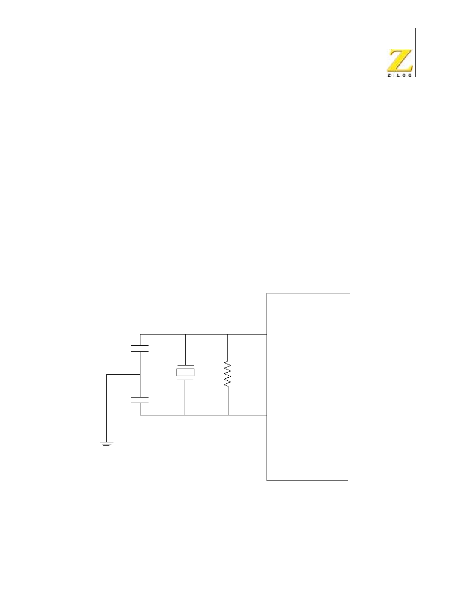
eZ80190 Product Specification
PS006611-0703
PRELIMINARY
Crystal Oscillator
177
Crystal Oscillator
The eZ80190 device features an on-chip crystal oscillator that supplies clocks to
the internal eZ80
Æ
CPU core, to peripherals, and to the external pin. The clock cir-
cuitry uses the three dedicated pins X
IN
, X
OUT
, and PHI.
The external clock/oscillator (X
IN
) input features two clock-generation options. X
IN
may be used to interface the internal oscillator to an external oscillator (see
Figure 35). Typical circuit parameters are C1 = C2 = 10
pF and R = 1
M
using a a
parallel resonant crystal.
X
IN
can also accept a CMOS-level clock input. The oscillator output (X
OUT
) con-
nects the internal crystal oscillator to an external crystal oscillator. If an external
clock is used, X
OUT
should be left unconnected. The PHI pin, which drives the
high-speed system clock, may be used to synchronize other peripherals to the
eZ80190 device system clock.
Note: *These values are typical values only. Actual values must be tuned for the crystal and the
frequency of operation.
Figure 35. Crystal Oscillator
C2
C1
R
X
IN
X
OUT
eZ80190
10pF*
10pF*
1M
*

eZ80190 Product Specification
PS006611-0703
PRELIMINARY
Electrical Characteristics
178
Electrical Characteristics
Absolute Maximum Ratings
Stresses greater than those listed in Table 112 may cause permanent damage to
the device. These ratings are stress ratings only. Operation of the device at any
condition outside those indicated in the operational sections of these specifica-
tions is not implied. Exposure to absolute maximum rating conditions for extended
periods may affect device reliability. For improved reliability, unused inputs should
be tied to one of the supply voltages (V
DD
or V
SS
).
Table 112. Absolute Maximum Ratings
Parameter
Min
Max
Units
Notes
Ambient temperature under bias
≠40
+105
C
1
Storage temperature
≠65
+150
C
Voltage on any pin with respect to V
SS
≠0.3
+6.0
V
2
Voltage on V
DD
pin with respect to V
SS
≠0.3
+6.0
V
Total power dissipation
520
mW
Maximum current out of V
SS
145
mA
Maximum current into V
DD
145
mA
Maximum output current from active output pin
≠8
+8
mA
Notes:
1. Operating temperature is specified in
Table 113
.
2. This voltage applies to all pins except where otherwise noted.

eZ80190 Product Specification
PS006611-0703
PRELIMINARY
DC Characteristics
179
DC Characteristics
Table 113 lists the Direct Current characteristics of the eZ80190 device.
In the following pages, Figure 36 illustrates the typical current consumption of the
eZ80190 device versus the number of WAIT states while operating 25∫C, 3.3
V,
and with either a 1-MHz or 5-MHz system clock. Figure 37 illustrates the typical
current consumption of the eZ80190 device versus the number of WAIT states
while operating 25∫C, 3.3
V, and with either a 20-MHz or 50-MHz system clock.
Figure 38 illustrates the typical current consumption of the eZ80190 device versus
the system clock frequency while operating 25∫C, 3.3
V, and using 0, 2, or 7 WAIT
states. Figure 39 illustrates the typical current consumption of the eZ80190 device
versus the system clock frequency while operating at 3.3
V, 7 WAIT states, and
with either a 5-MHz, 20-MHz, or 50-MHz system clock.
Table 113. DC Characteristics
Symbol Parameter
Standard
Temperature Range
= 0∫C to 70∫C
Extended
Temperature Range
= ≠40∫C to 105∫C
Units Conditions
Min
Max
Min
Max
V
DD
Supply Voltage
3.0
3.6
3.0
3.6
V
V
IL
Low Level
Input Voltage
≠0.3
0.8
V
≠0.3
0.8
V
V
V
IH
High Level
Input Voltage
0.7
x
V
DD
5.5
0.7
x
V
DD
5.5
V
V
OL
Low Level
Output Voltage
0.4
0.4
V
V
DD
= 3.0V;
I
OL
= 1mA
V
OH
High Level
Output Voltage
2.4
2.4
V
V
DD
= 3.0V;
I
OH
= ≠1mA
I
IL
Input Leakage
Current
≠10
+10
≠10
+10
µA
V
DD
= 3.6V;
V
IN
= V
DD
or V
SS
*
I
TL
Tri-State Leakage
Current
≠10
+10
≠10
+10
µA
V
DD
= 3.6V
Note: *This condition excludes the ZDA and ZCL pins, when driven Low, due to the presence of on-chip pull-ups.
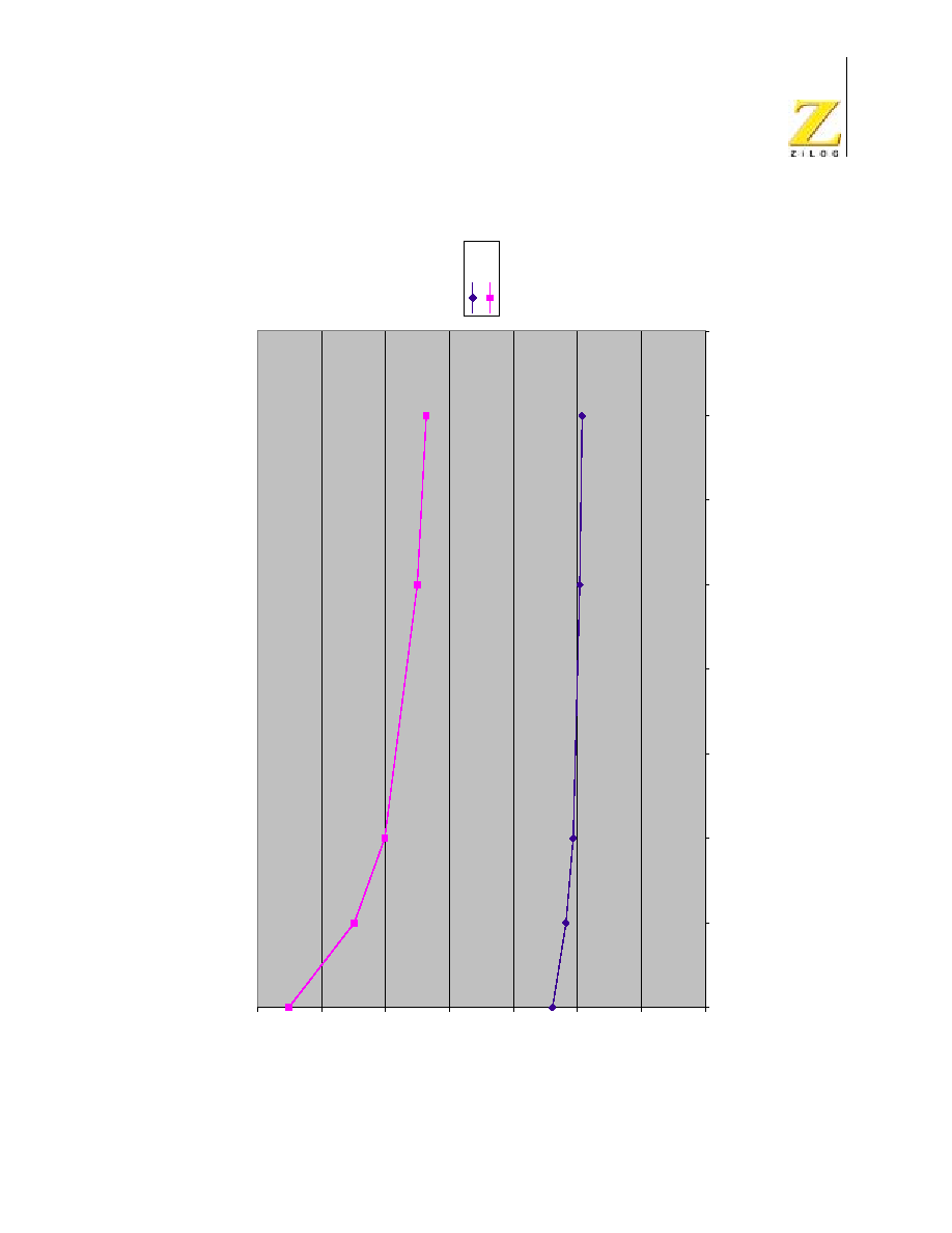
eZ80190 Product Specification
PS006611-0703
PRELIMINARY
DC Characteristics
180
Figure 36. I
CC
vs. WAIT1
ICC vs. WAIT States (Typical @ 3.3V, 25C)
0.00
2.00
4.00
6.00
8.00
10.00
12.00
14.00
012
3456
78
WAIT States
Current (mA)
1MHZ
5MHz

eZ80190 Product Specification
PS006611-0703
PRELIMINARY
DC Characteristics
181
Figure 37. I
CC
vs. WAIT2
ICC vs WAIT States (Typical @ 3.3V, 25C)
0.00
20.00
40.00
60.00
80.00
100.00
120.00
01
23
45
67
8
WAIT States
Current (mA)
20MHz
50MHz

eZ80190 Product Specification
PS006611-0703
PRELIMINARY
DC Characteristics
182
Figure 38. I
CC
vs. Frequency
ICC vs. Frequency (Typical @3.3V, 25C)
0.00
20.00
40.00
60.00
80.00
100.00
120.00
01
0
2
0
3
0
4
05
06
0
Frequency (MHz)
Current (mA)
0 WAIT
2 WAIT
7 WAIT
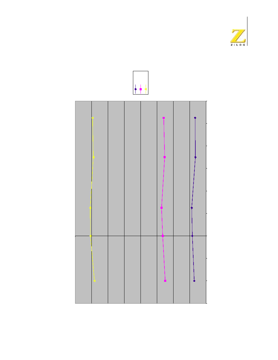
eZ80190 Product Specification
PS006611-0703
PRELIMINARY
DC Characteristics
183
Figure 39. I
CC
vs. Temperature
ICC vs. Temp (Typical @ 3.3V, 7 WAIT States)
0.00
10.00
20.00
30.00
40.00
50.00
60.00
70.00
80.00
-60
-40
-20
0
2
0
4
0
6
0
8
0
100
120
Temperature (C)
Current (mA)
5MHz
20MHz
50MHz

eZ80190 Product Specification
PS006611-0703
PRELIMINARY
AC Characteristics
184
AC Characteristics
The section provides information on the Alternating Current (AC) characteristics
and timing of the eZ80190 device. All AC timing information assumes a standard
load of 50
pF on all outputs.
External Memory Read Timing
Figure 40 and Table 115 diagram the timing for external READs.
Table 114. AC Characteristics
Symbol
Parameter
T
A
= 0
0
C to 70
0
C
T
A
= ≠40
0
C to 105
0
C
Units Conditions
Min
Max
Min
Max
T
XIN
System Clock
Cycle Time
20
20
ns
V
DD
= 3.0≠3.6V
T
XINH
System Clock
High Time
8
8
ns
V
DD
= 3.0≠3.6V;
T
CLK
= 20
ns
T
XINL
System Clock
Low Time
8
8
ns
V
DD
= 3.0≠3.6V;
T
CLK
= 20
ns
T
XINR
System Clock
Rise Time
2
2
ns
V
DD
= 3.0≠3.6V;
T
CLK
= 20
ns
T
XINF
System Clock
Fall Time
2
2
ns
V
DD
= 3.0≠3.6V;
T
CLK
= 20
ns
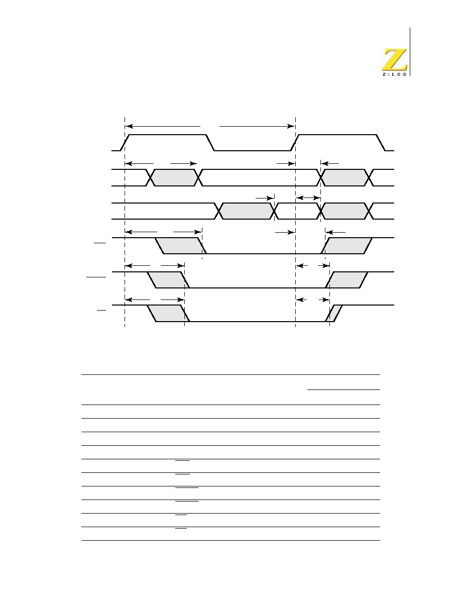
eZ80190 Product Specification
PS006611-0703
PRELIMINARY
AC Characteristics
185
Figure 40. External Memory Read Timing
Table 115. External Read Timing
Parameter
Description
Delay (ns)
Min.
Max.
T
1
Clock Rise to ADDR Valid Delay
--
10.2
T
2
Clock Rise to ADDR Hold Time
1.6
--
T
3
Clock Rise to Output DATA Valid Delay
0.0
--
T
4
DATA Hold Time from Clock Rise
5.0
--
T
5
Clock Rise to CSx Assertion Delay
3.0
10.5
T
6
Clock Rise to CSx Deassertion Delay
3.0
9.7
T
7
Clock Rise to MREQ Assertion Delay
2.8
9.6
T
8
Clock Rise to MREQ Deassertion Delay
1.6
6.9
T
9
Clock Rise to RD Assertion Delay
3.0
9.8
T
10
Clock Rise to RD Deassertion Delay
2.5
7.1
X
ADDR[23:0]
DATA[7:0]
(input)
CSx
MREQ
RD
IN
T
1
T
2
T
3
T
4
T
8
T
6
T
10
T
7
T
5
T
9
T
CLK
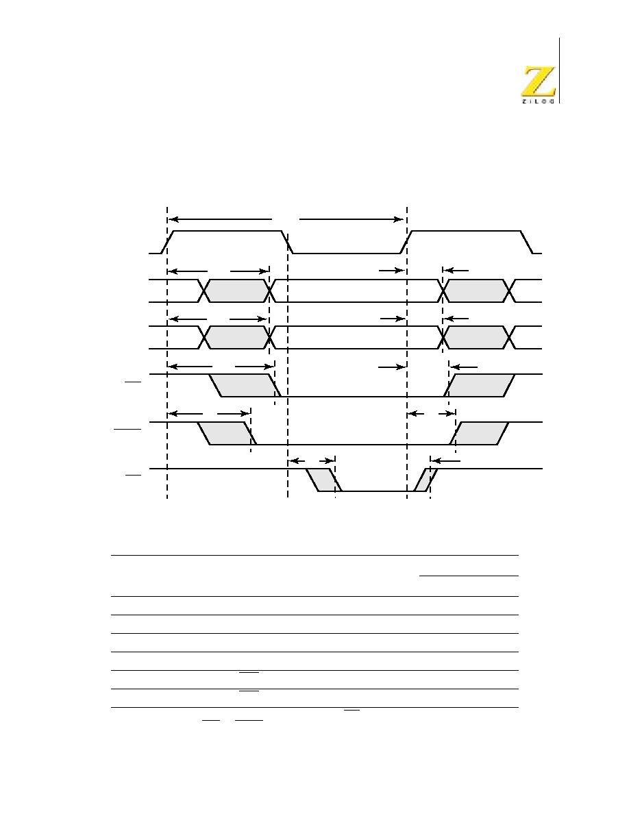
eZ80190 Product Specification
PS006611-0703
PRELIMINARY
AC Characteristics
186
External Memory Write Timing
Figure 41 and Table 116 diagram the timing for external writes.
Figure 41. External Memory Write Timing
Table 116. External Write Timing
Parameter
Description
Delay (ns)
Min.
Max.
T
1
Clock Rise to ADDR Valid Delay
--
10.2
T
2
Clock Rise to ADDR Hold Time
1.6
--
T
3
Clock Rise to Output DATA Valid Delay
--
10.2
T
4
DATA Hold Time from Clock Rise
5.0
--
T
5
Clock Rise to CSx Assertion Delay
3.0
10.5
T
6
Clock Rise to CSx Deassertion Delay
3.0
9.7
Note: *At the conclusion of a write cycle, deassertion of WR always occurs before any change to
ADDR, DATA, CSx, or MREQ.
X
ADDR[23:0]
DATA[7:0]
(output)
CSx
MREQ
WR
IN
T
1
T
2
T
3
T
4
T
8
T
6
T
10
T
7
T
5
T
9
T
CLK
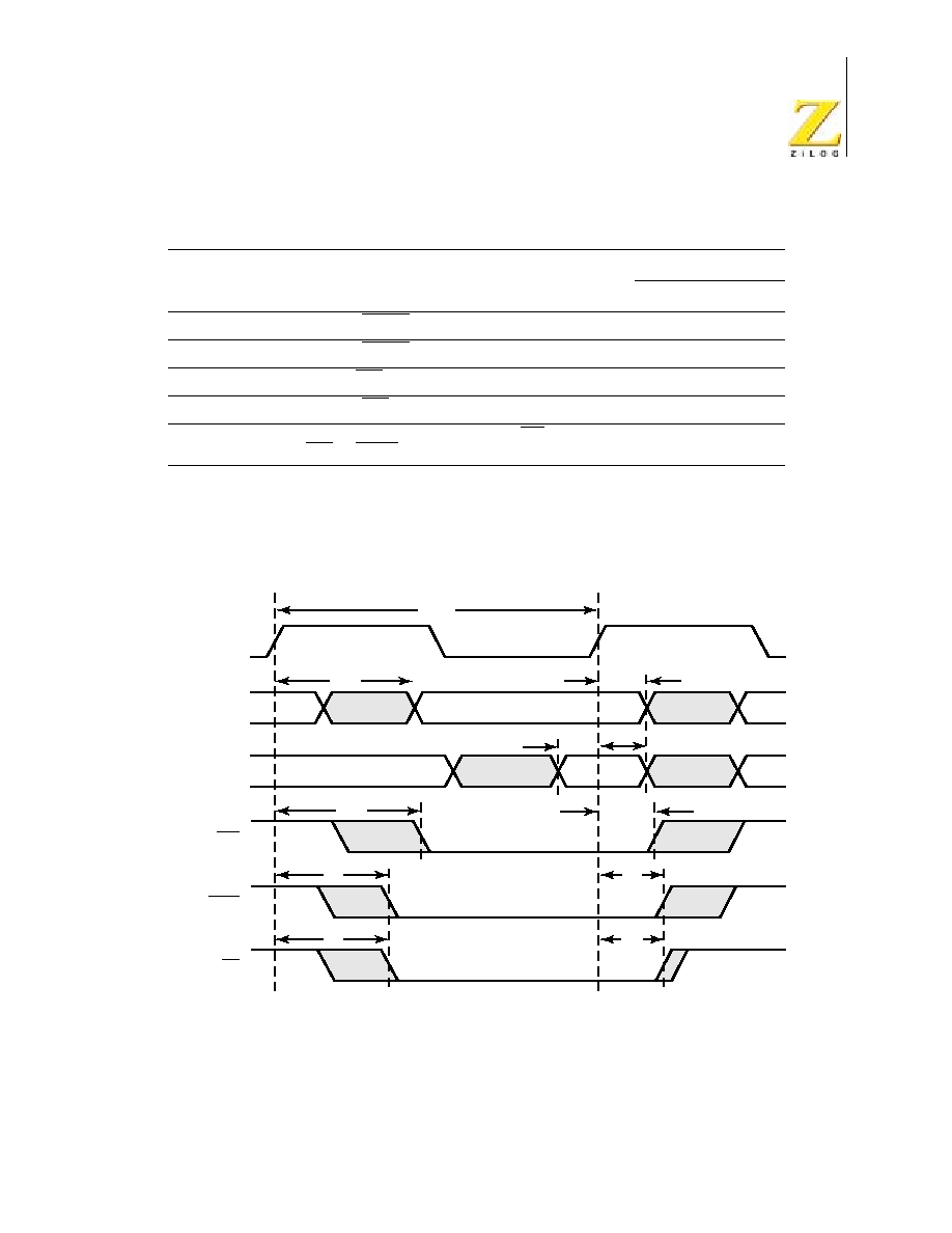
eZ80190 Product Specification
PS006611-0703
PRELIMINARY
AC Characteristics
187
External I/O Read Timing
Figure 42 and Table 117 diagram the timing for external I/O reads.
T
7
Clock Rise to MREQ Assertion Delay
2.8
9.6
T
8
Clock Rise to MREQ Deassertion Delay
1.6
6.9
T
9
Clock Fall to WR Assertion Delay
1.5
3.9
T
10
Clock Rise to WR Deassertion Delay*
1.4
4.1
Figure 42. External I/O Read Timing
Table 116. External Write Timing (Continued)
Parameter
Description
Delay (ns)
Min.
Max.
Note: *At the conclusion of a write cycle, deassertion of WR always occurs before any change to
ADDR, DATA, CSx, or MREQ.
X
ADDR[23:0]
DATA[7:0]
(input)
CSx
IORQ
RD
IN
T
1
T
2
T
3
T
4
T
8
T
8
T
10
T
7
T
5
T
9
T
CLK

eZ80190 Product Specification
PS006611-0703
PRELIMINARY
AC Characteristics
188
External I/O Write Timing
Figure 43 and Table 118 diagram the timing for external I/O writes.
Table 117. External I/O Read Timing
Parameter
Description
Delay (ns)
Min
Max
T
1
Clock Rise to ADDR Valid Delay
--
10.2
T
2
Clock Rise to ADDR Hold Time
1.6
--
T
3
Input DATA Valid to Clock Rise Setup Time
0.0
--
T
4
DATA Hold Time from Clock Rise
5.0
--
T
5
Clock Rise to CSx Assertion Delay
3.0
10.5
T
6
Clock Rise to CSx Deassertion Delay
3.0
9.7
T
7
Clock Rise to IORQ Assertion Delay
2.1
10.3
T
8
Clock Rise to IORQ Deassertion Delay
4.1
7.9
T
9
Clock Rise to RD Assertion Delay
3.0
9.8
T
10
Clock Rise to RD Deassertion Delay
2.5
7.1
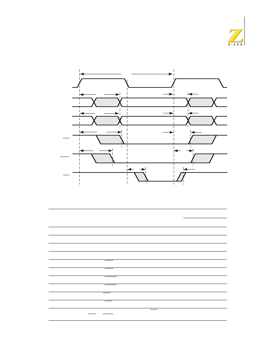
eZ80190 Product Specification
PS006611-0703
PRELIMINARY
AC Characteristics
189
Figure 43. External I/O Write Timing
Table 118. External I/O Write Timing
Parameter
Description
Delay (ns)
Min
Max
T
1
Clock Rise to ADDR Valid Delay
--
10.2
T
2
Clock Rise to ADDR Hold Time
1.6
--
T
3
Clock Rise to Output DATA Valid Delay
--
10.2
T
4
DATA Hold Time from Clock Rise
5.0
--
T
5
Clock Rise to CSx Assertion Delay
3.0
10.5
T
6
Clock Rise to CSx Deassertion Delay
3.0
9.7
T
7
Clock Rise to IORQ Assertion Delay
2.1
10.3
T
8
Clock Rise to IORQ Deassertion Delay
4.1
7.9
T
9
Clock Fall to WR Assertion Delay
1.5
3.9
T
10
Clock Rise to WR Deassertion Delay*
1.4
4.1
Note: *At the conclusion of a write cycle, deassertion of WR always occurs before any change to
ADDR, DATA, CSx, or IORQ.
X
ADDR[23:0]
DATA[7:0]
(output)
CSx
IORQ
WR
IN
T
1
T
2
T
3
T
4
T
8
T
6
T
10
T
7
T
5
T
9
T
CLK
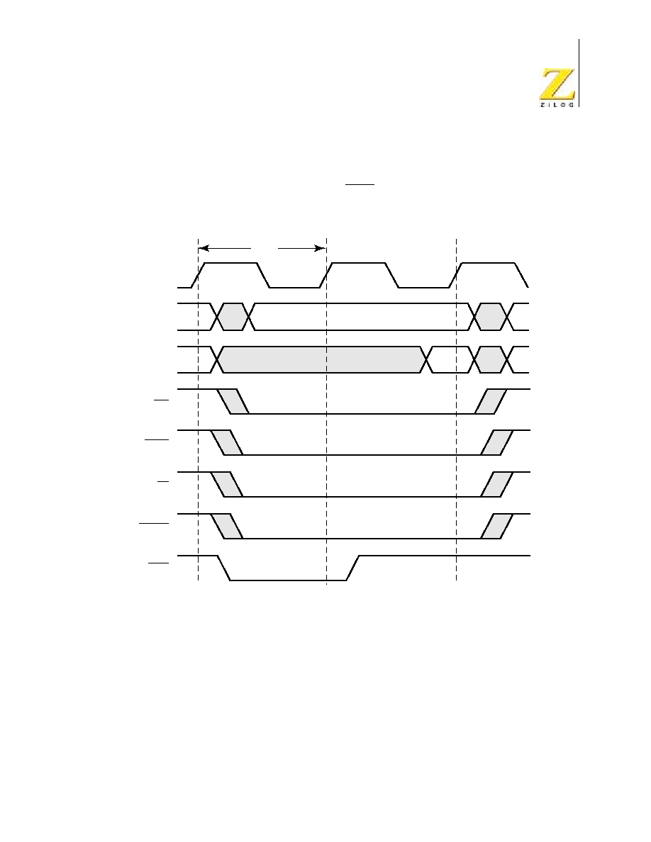
eZ80190 Product Specification
PS006611-0703
PRELIMINARY
AC Characteristics
190
Wait State Timing for Read Operations
Figure 44 illustrates the extension of the memory access signals using a single
WAIT state for a read operation. The WAIT signal is not delivered to a pin on the
eZ80190 device. It is illustrated here for informational purposes only.
Figure 44. Wait State Timing for Read Operations
T
CLK
X
ADDR[23:0]
DATA[7:0]
(output)
CSx
MREQ
RD
IN
WAIT
INSTRD
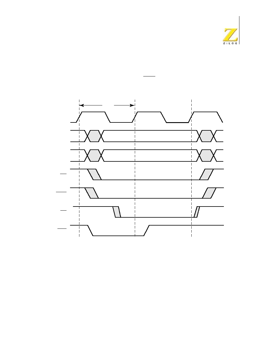
eZ80190 Product Specification
PS006611-0703
PRELIMINARY
AC Characteristics
191
Wait State Timing for Write Operations
Figure 45 illustrates the extension of the memory access signals using a single
WAIT state for a write operation. The WAIT signal is not delivered to a pin on the
eZ80190 device and is illustrated here for informational purposes only.
Figure 45. Wait State Timing for Write Operations
T
CLK
X
ADDR[23:0]
DATA[7:0]
(output)
CSx
MREQ
WR
IN
WAIT
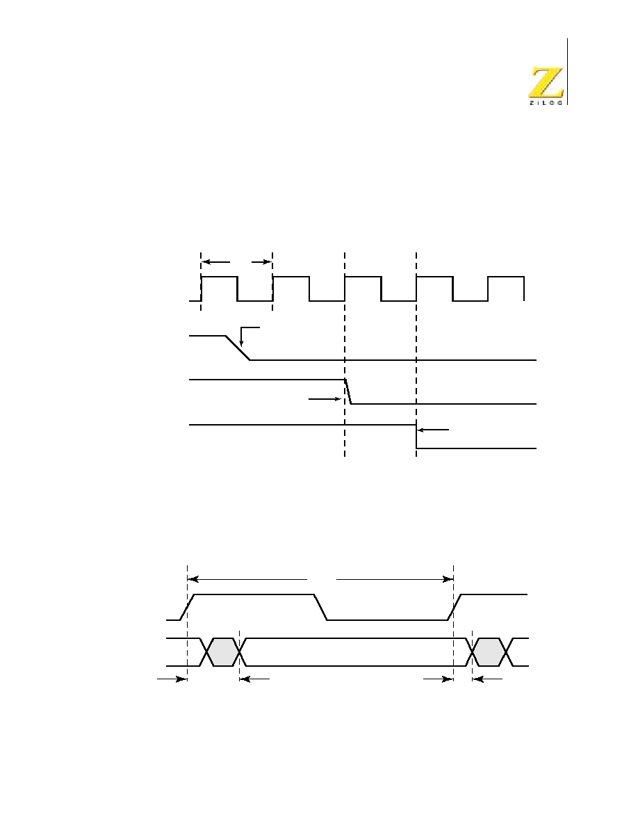
eZ80190 Product Specification
PS006611-0703
PRELIMINARY
AC Characteristics
192
General Purpose I/O Port Input Sample Timing
Figure 46 illustrates timing of the GPIO input sampling. The input value on a GPIO
port pin is sampled on the rising edge of the system clock. The port value is then
available to the CPU on the second rising clock edge following the change of the
port value.
General Purpose I/O Port Output Timing
Figure 47 and Table 119 indicate the timing of the GPIO outputs.
Figure 46. Port Input Sample Timing
Figure 47. GPIO Port Output Timing
T
CLK
System
Clock
GPIO Pin
Input Value
GPIO Input
Data Latch
GPIO Data
READ on Data Bus
Port Value
Changes to 0
0 Latched
Into GPIO
Data Register
GPIO Data Register
Value 0 Read
by eZ80
T
CLK
EXTAL
Port Output
T
1
T
2

eZ80190 Product Specification
PS006611-0703
PRELIMINARY
AC Characteristics
193
External Bus Acknowledge Timing
Table 120 provides bus acknowledge timing details.
External System Clock Driver Timing
Table 121 provides timing information for the PHI pin. The PHI pin allows external
peripherals to synchronize with the internal system clock driver on the eZ80190
device.
Table 119. GPIO Port Output Timing
Parameter
Description
Delay (ns)
Min
Max
T
1
Clock Rise to Port Output Valid Delay
--
8.9
T
2
Clock Rise to Port Output Hold Time
1.8
--
Table 120. Bus Acknowledge Timing
Parameter
Description
Delay (ns)
Min
Max
T
1
Clock Rise to BUSACKN Assertion Delay
--
6.5
T
2
Clock Rise to BUSACKN Deassertion Delay
2.3
--
Table 121. PHI System Clock Timing
Parameter
Description
Delay (ns)
Min
Max
T
1
Clock Rise to PHI Rise
1.8
4.0
T
2
Clock Fall to PHI Fall
2.0
4.8
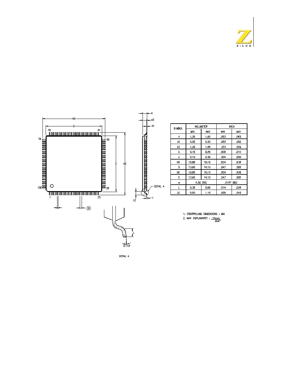
eZ80190 Product Specification
PS006611-0703
PRELIMINARY
Packaging
194
Packaging
Figure 48 illustrates the 100-pin LQFP (also called the VQFP) package for the
eZ80190 device.
Figure 48. 100-Pin LQFP Package

eZ80190 Product Specification
PS006611-0703
PRELIMINARY
Ordering Information
195
Ordering Information
Table 122 provides a part number, a product specification index code, and a brief
description of each eZ80190 part.
Navigate your browser to ZiLOG's website to order the eZ80190 device. Or, con-
tact your local
ZiLOG Sales Office
. ZiLOG provides additional assistance on its
Customer Service
page, and is also here to help with
Technical Support
issues.
For ZILOG's valuable
software development tools
and
downloadable software
,
visit the
ZiLOG website
. Download the latest release of
ZiLOG Developer Studio
!
Part Number Description
ZiLOG part numbers consist of a number of components, as indicated in the fol-
lowing examples:
Example. Part number eZ80190AZ050SC is an eZ80
Æ
CPU product in an LQFP
package, operating with a 50-MHz external clock frequency over a 0∫C to +70∫C
temperature range, and built using the Plastic Standard environmental flow.
Table 122. Ordering Information
Part
PSI
Description
eZ80190
eZ80190AZ050SC
100-pin LQFP, 50
MHz, Standard Temperature
eZ80190AZ050EC
100-pin LQFP, 50
MHz, Extended Temperature
eZ80190 Development Kit
eZ8019000100ZCO
Complete Development Kit
ZiLOG Base Products
eZ80
eZ80
Æ
CPU ZiLOG prefix
190
Product Number
AZ
Package
050
Speed
S or E
Temperature
C
Environmental Flow
Package
AZ = LQFP (also called the VQFP)
Speed
050 = 50 MHz
Standard Temperature
S = 0∫C to +70∫C
Extended Temperature
E = ≠40∫C to +105∫C
Environmental Flow
C = Plastic Standard

eZ80190 Product Specification
PS006611-0703
PRELIMINARY
Document Information
196
Document Information
Document Number Description
The Document Control Number that appears in the footer on each page of this
document contains unique identifying attributes, as indicated in the following
table:
Change Log
PS
Product Specification
0066
Unique Document Number
10
Revision Number
0703
Month and Year Published
Rev
Date
Purpose
By
01
09/00
Original issue
W. Wootton/T. Sierer
02
01/01
Format revision
G. Gamble
03
05/01
Content revision
D. Wilson/R. Beebe
04
08/01
Content additions
D. Wilson/R. Beebe
05
08/01
Minor content revision
D. Wilson/R. Beebe
06
10/01
Minor content revision
D. Wilson/R. Beebe
07
10/01
Minor content revision
D. Wilson/R. Beebe
08
12/01
Minor content revision
D. Wilson/R. Beebe
09
07/02
Changes to max. ratings
J. Eversmann/R. Beebe
10
12/02
Characterization data revision
B. Metzler/R. Beebe
11
07/03
Correction to Timer0 Reload Reg. J. Neville

eZ80190 Product Specification
PS004601-0301
P R E L I M I N A R Y
Index
197
Index
Numerics
100-pin LQFP package 4, 194
16-bit divisor count 62≠63
16-bit downcounter 31, 61
16-bit reload register 31
16-bit start value 33
16-MB linear addressing 30
24-bit address bus 22
24-bit address mode 30
4-bit clock prescaler 31
A
Absolute Maximum Ratings 178
AC Characteristics 184
ACK--see Acknowledge
ACK bit 100
Acknowledge 91≠92, 96≠97, 99≠100, 102≠
103, 105, 107≠108
I
2
C 91
ADDR0 6
ADDR1 6
ADDR2 6
ADDR3 6
ADDR4 6
ADDR5 6
ADDR6 7
ADDR7 7
ADDR8 7
ADDR9 7
ADDR10 7
ADDR11 8
ADDR12 8
ADDR13 8
ADDR14 8
ADDR15 8
ADDR16 9
ADDR17 9
ADDR18 9
ADDR19 9
ADDR20 9
ADDR21 9
ADDR22 10
ADDR23 10
address bus 6≠10, 52, 54, 55, 136
24-bit 22
address match 52, 56, 149, 153
ZDI Registers 154≠158
Addressing 102
ADL MEMORY mode 52, 137≠138, 155, 160,
165
bit 137≠138
ADL Mode--see ADL MEMORY mode
alternate-function I/O 45, 60
Alternatives to OTI2R and INI2R 115
AND connection 93
Arbitration 95≠100, 101, 104, 107≠108
Architectural Overview 1
Arithmetic Instructions 166
asynchronous communications protocol 65≠66
bits 67
Asynchronous Receiver/Transmitter 60
asynchronous reception protocol 66
asynchronous serial data 14, 17
asynchronous transmission protocol 66
auto-address increment function 161
automatic reload 35≠38
B
Baud Rate Generator 61
Functional Description 61
output 61
bidirectional serial protocol 147
BI--see Break Indication 78
bit generation and detection, parity 65
bit generation and detection, start 65
bit generation and detection, stop 65
Bit Manipulation Instructions 166
block data transfer 139

eZ80190 Product Specification
PS004601-0301
P R E L I M I N A R Y
Index
198
Block Diagram 2
Block Transfer and Compare Instructions 166
Break Indication 68, 78
break signal 67, 75
BRG--see Baud Rate Generator
BRG clock 67
divisor ratio 61, 63
BRG counter 61≠63
BRG Divisor Latch 62≠63
BRG Divisor Latch registers 61
High Byte 63
Low Byte 62
BRG divisor value 61≠64
BRG output frequency 61
BRGx 61
BRGx_DLR_H 61≠63
BRGx_DLR_H register 72
BRGx_DLR_L 61≠63
BRGx_DLR_L register 62, 71
BURST mode 139≠140, 144
bus acknowledge 20
bus arbitration 90, 94
Bus Arbitration Overview 90
Bus Clock Speed 110
Bus Enable bit 105≠106
bus request 20≠21, 139
BUSACK--see bus acknowledge
BUSREQ--see bus request
Byte Format 91
byte transfer 90≠91, 95
cycle-steal 141
C
C register 114
CALC bank 112, 114≠118, 121≠122, 125, 134,
135
CALC_STAT field 115
CGE bit 101
Change Log 196
Characteristics, Electrical
Absolute Maximum Ratings 178
Chip Select Registers 54
Chip Select signal 50, 54≠55
Chip Select signals, external 58
Chip Select x Lower Bound Register 54
Chip Select x Upper Bound Register 55
Chip Select/Wait State Generator block 6≠10
Chip Select/Wait State Generator, Register
Map 24≠25
Chip Selects and Wait States 49
Chip Selects, external I/O 22
Chip Selects, I/O 49, 52, 54≠55
Chip Selects, Memory 49
Clear to Send 15, 18, 80
Delta Status Change of 80
clock divider 34≠35, 83, 109
clock divider ratio 32
clock frequency 32
16X 69
50-MHz external 195
eZ80 CPU 147
clock generator 60, 82
clock period 45, 46, 90
clock prescaler, 4-bit 31
clock source 61
Clock Synchronization 93
for Handshake 95
Clocking Overview 90
CONTINUOUS mode 31, 33≠35, 37≠38
control register values 50, 115
Control Transfers 69
CPHA--see SPI Clock Phase 83≠84, 86≠87
CPOL--see SPI Clock Polarity 83≠85, 87
Crystal Oscillator 177
CS_EN 49, 52, 56
CS_IO 49, 52, 54, 56
CS0 5
CS1 5
CS2 5
CS3 5
CTS--see Clear to Send 77, 80
CTS0 18
CTS1 15
current count value 34, 36
Customer Feedback Form 210
Customer Information 210
CYCLE-STEAL mode 139≠141, 144

eZ80190 Product Specification
PS004601-0301
P R E L I M I N A R Y
Index
199
D
DATA bank 112, 114≠118, 121≠122, 125,
134≠135
data bus 10, 57, 111
Data Carrier Detect 16, 19, 77, 80
Delta Status Change of 80
Data Ready 79
data ready interrupt, receiver 68
data ready logic, receiver 67
Data Set Ready 16, 19, 80
Delta Status Change of 80
Data Terminal Ready 15, 18, 77
Data Transfers 69
Data Validity 91
data_stat field 115
DATA0 10
DATA1 10
DATA2 10
DATA3 10
DATA4 11
DATA5 11
DATA6 11
DATA7 11
DC Characteristics 179
DCD--see Data Carrier Detect
DCD0 19
DCD1 16
DCTS--see Clear to Send, Delta Status
Change of 80
DDCD--see Data Carrier Detect, Delta Status
Change of 80
DDSR--see Data Set Ready, Delta Status
Change of 80
debugging 146
Defining A New Calculation As READY 114
Defining The DATA Bank As EMPTY 114
Direct Memory Access 139
divisor count, 16-bit 62≠63
DMA--see Direct Memory Access
DMA Channel Priorities 140
DMA Control Registers 141
DMA controller 139≠141, 144
DMA controllers, internal 21
DMA Controllers, Register Map 28≠29
DMA Interrupts 141
DMA Programming 139
DMA Transfer Modes 140
Document Information 196
Document Number Description 196
downcounter 36
16-bit 31, 61
DR--see Data Ready 67, 79
DR bit 44
DSP operations 118
DSR--see Data Set Ready 77, 80
DSR0 19
DSR1 16
DTR--see Data Terminal Ready 77
DTR0 18
DTR1 15
dual-edge-triggered interrupt mode 45, 47
dual-port MACC RAM 57, 111, 122
E
edge-detected interrupt 47
edge-selectable interrupt 47
edge-triggered interrupt mode 45
Edge-Triggered Interrupts 47
EI--see Interrupt Enable
EI, Op Code Map 170
Electrical Characteristics 178
ENAB--see Bus Enable bit
Enabling 40
Disabling The WDT 40
Ending Program Counter 137≠138
end-of-count value, PRT 32≠35
Environmental Flow 195
ERR bit 69, 78
Exchange Instructions 167
Extended Temperature 195
External I/O Read Timing 187
External I/O Write Timing 188
External Memory Read Timing 184
External Memory Write Timing 186
external NMI signal 11
external pull-down resistor 45

eZ80190 Product Specification
PS004601-0301
P R E L I M I N A R Y
Index
200
eZ80
Æ
CPU Core 30
Features 30
Overview 30
eZ80
Æ
CPU Instruction Set 30, 166
F
Fall Time, system clock 184
FAST mode 90, 110
Features 1
FE--see Framing Error
FIFO mode 66, 68
four-wire interface 82
framing error 67, 72, 78≠79
detection 65
full-duplex transmission 82, 84
G
General Call Address 90, 101, 103, 105, 108
General-Purpose Input/Output 43
control register bits 43
Control Registers 47
Interrupts 46
Mode 1 44
Mode 2 44, 45
Mode 3 44
Mode 4 44
Mode 5 45
Mode 6 45, 47
Mode 7 45
Mode 8 45
Mode 9 45, 47
mode control registers 43
Operation 43
Overview 43
Port Sample Timing 192
Ports 24, 43
Ports, Register Map 23
GND 2
GPIO--see General-Purpose Input/Output
H
HALT 11
hand-shake capability 65
high-impedance output 44≠45
I
I/O Chip Select Operation 52
I/O Chip Select Precaution 52
I/O Chip Selects 49, 52, 54≠55
external 22
I/O space 6≠10, 12, 49, 52
eZ80 CPU 111
eZ80 Webserver 115
I
2
C--see Inter-Integrated Circuit serial bus
I
2
C Acknowledge 91
bit 100, 105
I
2
C bus 90
protocol 91
I
2
C Clock Control Register 108
I
2
C Control Register 104
I
2
C Data Register 104
I
2
C Extended Slave Address Register 103
I
2
C General Characteristics 90
I
2
C Registers 102
I
2
C Serial Clock 14, 90≠95, 108
I
2
C Serial Data 90≠92, 94, 101
I
2
C Serial I/O Interface 90
I
2
C Slave Address Register 102
I
2
C Software Reset Register 110
I
2
C Status Register 107
I
2
Cx 96
I
2
Cx_CTL register 90, 95, 98, 100≠102, 104,
107≠108
I
2
Cx_DR register 95, 98, 100≠101, 104≠105
I
2
Cx_SAR byte 102≠103
I
2
Cx_SR register 95≠102, 107
I
2
Cx_xSAR register 103
IDLE state 85, 90, 96≠101, 105, 108
SCK 84
IEN--see Interrupt Enable bit
IFLG bit 90, 95, 98, 100≠102, 105, 107≠108
IM 0, Op Code Map 173
IM 1, Op Code Map 173

eZ80190 Product Specification
PS004601-0301
P R E L I M I N A R Y
Index
201
IM 2, Op Code Map 173
IN_SHIFT and OUT_SHIFT 118
IN_SHIFT Function 119
in-circuit emulation 146
INI2R block 113≠114
INI2R instruction 113≠114, 118, 122
initial count value 32, 42
Input/Output Instructions 167
Input/Output Request 5, 12
INSTRD--see Instruction READ
Instruction READ 5, 12, 53
Instruction Store 4
0 Registers 160
Inter-Integrated Circuit serial bus 60
internal DMA controllers 21
internal pull-up 12, 44
internal RAM 50, 58
Interrupt Controller 136
Interrupt Enable 11, 129
interrupt enable bit 68, 104≠106, 141
interrupt enable flag 34
Interrupt Enable Flag 1 164
Interrupt Enable Register, UART0 25
Interrupt Enable Register, UART1 26
Interrupt Enable Register, UARTx 72
Interrupt Enable, PRT 33, 34
interrupt input 12≠21
interrupt mode ,single-edge-triggered 45, 47
interrupt mode, dual edge-triggered 45, 47
interrupt mode, level-sensitive 45
interrupt service request 34
DMA 144
Interrupt Service Routine 136≠138
interrupt, edge-detected 47
interrupt, low-level 46
IORQ--see Input/Output Request
IRQ_EN 34, 35, 86≠87
ISR--see Interrupt Service Routine
L
least significant bit 36, 38, 67, 95≠96, 98, 101,
107, 119, 131, 147
least significant byte 119≠122, 132, 137≠138,
158
left-shift 119
level-sensitive interrupt 45, 47
level-triggered interrupts 46
Line break detection and generation 65
line status error 68
line status interrupt 68, 70, 72
Load Instructions 167
Logical Instructions 168
LOOP-BACK mode 77, 80
low-level interrupt 46
LSB--see least significant byte
lsb--see least significant bit
M
MACC--see Multiply-Accumulator
MACC Accumulator Byte 0 Register 132
MACC Accumulator Byte 1 Register 132
MACC Accumulator Byte 2 Register 133
MACC Accumulator Byte 3 Register 133
MACC Accumulator Byte 4 Register 134
MACC Control Register 129
MACC Dual Bank Operation 115
MACC Length Register 127
MACC Overview 111
MACC RAM 122
Address Indexing 122
dual-port 57
MACC Status Register 134
MACC x DATA Ending Address Register 126
MACC x DATA Reload Address Register 127
MACC y DATA Ending Address Register 128
MACC y DATA Reload Address Register 129
MACC_AC0 27, 114, 119≠121, 132
MACC_AC1 28, 114, 119≠121, 132
MACC_AC2 28, 114, 119≠121, 133
MACC_AC3 28, 114, 119≠121, 133
MACC_AC4 28, 114, 116≠121, 134
MACC_CTL 27, 114, 116≠120, 121, 129
MACC_LENGTH 27, 115, 121, 123
MACC_STAT 28, 114≠115, 117, 121, 134
MACC_xEND 27, 115, 121, 123, 126≠127

eZ80190 Product Specification
PS004601-0301
P R E L I M I N A R Y
Index
202
MACC_xRELOAD 27, 115, 121, 123, 127
MACC_xSTART 27, 115, 121, 123, 125
MACC_yEND 27, 115, 121, 123, 128≠129
MACC_yRELOAD 27, 115, 121, 123, 129
MACC_ySTART 27, 115, 121, 123, 128
maskable interrupt 11, 164
Master In Slave Out 14, 17, 82
MASTER mode 90, 100≠101, 105, 107≠110
start bit 95≠100, 102, 105≠106, 108
START condition 106
START TRANSMIT condition 106
stop bit 98≠100, 102, 105≠106, 108
STOP condition 106
STOP TRANSMIT condition 106
MASTER mode, SPI 85
Master Out Slave In 14, 17, 82≠84, 86
Master Receive 90, 98
Status Codes for Data Bytes, I
2
C 100
Status Codes, I
2
C 98
master receiver 92, 100
MASTER TRANSMIT mode 90, 95, 100
Status Codes for Data Bytes, I
2
C 97
Status Codes, I
2
C 96
master transmitter 101
MASTER_EN 86≠87
MBASE 137, 155, 159, 161, 165
offset value 52
Memory and I/O Chip Selects 49
Memory Chip Select Example 50
Memory Chip Select Operation 49
Memory Chip Select Priority 50
Memory Chip Selects 49
Memory mode suffixes 160
Memory Request 5
memory space 6≠10, 49, 52
eZ80 CPU 111
MISO--see Master In Slave Out
MISO0 17
MISO1 14
Mode Fault 86
modem 67
control logic 67
control output 77
modem status 68, 70, 73, 77
input ports 77
inputs 67
Modem Status Interrupt, UART 69
Modem Status Register, UART 26≠27, 80
modem status signal 15≠16, 18≠19
MODF--see Mode Fault 83, 86, 88
Module Reset 69
MOSI--see Master Out Slave In
MOSI0 17
MOSI1 14
most significant bit 37≠38, 67, 82, 83, 91≠92,
104, 107, 120, 130, 147, 151
most significant byte 37≠38, 114, 119≠122,
134
MREQ--see Memory Request
MSB--see most significant byte
msb--see most significant bit
multimaster conflict 86, 88
Multiply-Accumulator 57, 111, 113, 114, 115,
118, 122, 134
Basic Operation 112
Control And Data Registers 125
RAM 58
Multiply-Accumulator, Register Map 27≠28
N
NACK--see Not Acknowledge
NMI--see Nonmaskable Interrupt
NMI input 11
NMI signal 11
NMI_OUT 40≠41
NO ERROR condition 70
NOISE bit 119, 129, 131
NOISE field 119
NOISE value 119
Nonmaskable Interrupt 11, 30, 39≠41, 168
Not Acknowledge 90, 92, 96≠101, 105, 108
O
OE--see overrun error
On-chip peripherals

eZ80190 Product Specification
PS004601-0301
P R E L I M I N A R Y
Index
203
on-chip peripherals 22, 52
On-chip RAM 49, 57≠59
Control, Register Map 25
Op-Code Map 170
open-drain I/O 12, 44
open-drain output 12≠21, 44, 90
open-source I/O 44
open-source mode 45
open-source output 12≠21
Operating Modes 95
Operation Of The eZ80190 Webserver During
ZDI Breakpoints 152
Ordering Information 195
Oscillator Input 19
Oscillator Output 19
OTI2R block 113≠114
OTI2R instruction 114, 116≠117, 121
OUT_SHIFT Function 120
OUT1--see modem control output 77, 80
OUT2--see modem control output 77, 80
overrun condition 65, 68, 89
overrun error 67, 72, 79
P
PA0 20
PA1 20
PA2 20
PA3 20
PA4 20
PA5 20
PA6 21
PA7 21
Packaging 194
parity bit 67, 72, 75, 79
generation and detection 65
parity checker 67
parity error 67, 75, 79
parity generator 66, 67
Part Number Description 195
PB0 12
PB1 12
PB2 12
PB3 13
PB4 13
PB5 13
PB6 13
PB7 13
PC0 14
PC1 14
PC2 15
PC3 15
PC4 15
PC5 16
PC6 16
PC7 16
PD0 17
PD1 17
PD2 18
PD3 18
PD4 18
PD5 19
PD6 19
PD7 19
PEN--see parity bit
PE--see parity error 79, 170
PHI--see system clock
Pin Description 4
Poll Mode Transfers 70
POP, Op Code Map 170, 172, 174
port pin value 45, 46
Port x Alternate Register 1 48
Port x Alternate Register 2 48
Port x Data Direction Registers 48
Port x Data Registers 47
Power connections 2
Problem Description or Suggestion 210
Processor Control Instructions 168
Product Information 210
Program Control Instructions 168
Programmable Reload Counter/Timers 22
Programmable Reload Timer duration 32
Programmable Reload Timer Operation 32
Programmable Reload Timers 31, 153
Programmable Reload Timers Overview 31
protocol, asynchronous communications 65≠
67
protocol, bidirectional serial 147

eZ80190 Product Specification
PS004601-0301
P R E L I M I N A R Y
Index
204
protocol, I
2
C bus 91
protocol, reception 66
PRT_EN bit 32
PRT_IRQ bit 34
PRT_IRQ--see timer interrupt flag
pull-down resistor, external 45
pull-up resistor, external 44, 90
pull-up resistor, internal 12, 44
PUSH, Op Code Map 170, 172, 174
R
RAM Address Upper Byte Register 57≠58
RAM Control Registers 58
Random Access Memory 57
RC rise times 11
RD--see READ instruction
READ instruction 5
Reading the Current Count Value 34
receive data ready condition 70
receive FIFO 66, 68, 71, 74
pointer 74
trigger level 74
receiver data ready interrupt event 68
receiver data ready logic 67
receiver interrupt 68
Receiver Interrupt, UART 68
receiver line error 67
Receiver overrun detection 65
receiver shift register 67, 79
Recommended Operation 121
Recommended Usage of the Baud Rate Gen-
erator 61
Register Map 22
Reload Register 22≠23, 27
reload register, 16-bit 31
Reload Value 32
Reload Value, PRT 33≠34
Reload Value, timer 32
reload value, timer 35, 37≠38
Request to Send 15, 18, 77
RESET 12, 168, 170
Or NMI Generation 40
Reset States 50
Resetting the I
2
C Registers 102
RETI--see Return from Interrrupt
RETN--see Return from Nonmaskable Inter-
rrupt
Retrieve A Calculation 122
Return from Interrrupt 137, 168, 173
Return from Nonmaskable Interrrupt 168, 173
Return Information 210
RI0 19
RI1 16
right-shift 120, 130
Ring Indicator 16, 19, 67, 77, 80
Trailing Edge Change on 80
rise time, RC 11
Rise Time, system clock 184
RI--see Ring Indicator
Rotate and Shift Instructions 169
RST--see RESET
RST_EN 36≠38
RST_FLAG 40
RTS--see Request to Send
RTS0 18
RTS1 15
RXD input signal 70≠71
RXD input start bit 67
RXD signal 67
RxD0 17
RxD1 14
S
SARx_CTL 142
Schmitt trigger 11≠12
SCK--see SPI Serial Clock
SCK0 18
SCK1 15
SCL--see I
2
C Serial Clock
SCL0 17
SCL1 14
scratch pad registers 81
SDA--see I
2
C Serial Data
SDA0 17
SDA1 14
selectable taps 31

eZ80190 Product Specification
PS004601-0301
P R E L I M I N A R Y
Index
205
serial bus 89
serial bus, I
2
C 60
serial bus, SPI 88
Serial Clock 83, 90
Serial Clock, I
2
C 14, 17, 90≠95, 108
Serial Clock, SPI 15, 18, 82≠83
serial communication controllers 60≠62
serial data 82≠83, 90
serial data, asynchronous 14, 17
Serial Data, I
2
C 14, 17, 90≠92, 94, 101
Serial Peripheral Interface 82
serial transmit/receive 66
Setting Timer Duration 32
Setting Up A New Calculation 121
Signal Direction 5
SINGLE PASS Mode 31≠32, 34≠35
single-edge-triggered interrupt mode 45, 47
SLAVE mode 82, 86, 90, 100, 102≠103, 105,
108
SLAVE RECEIVE mode 90, 94, 101
slave receiver 92, 95
Slave Select 15, 18, 82≠84, 86≠87
SLAVE TRANSMIT mode 90, 100, 105
slave transmitter 92, 98
Sleep instruction 166, 168, 173
SLP--see Sleep instruction
Software Control of the MACC 113
SPI--see Serial Peripheral Interface
SPI block 82
SPI Clock Phase 83≠84, 86≠87
SPI Clock Polarity 83≠85, 87
SPI Control Register 87
SPI Flags 85≠86, 89
SPI Functional Description 84
SPI interrupt 86
SPI MASTER mode 85
SPI Receive Buffer Register 86, 89
SPI Registers 86
SPI Serial Clock 15, 18, 82≠83
SPI Signals 82
SPI SLAVE mode 14, 17, 83, 86, 89
SPI Status Register 86, 88
SPI Transmit Shift Register 86, 88
SPI_EN 86≠87
SPIF--see SPI Flags
SPIx_CTL 85≠86
SPIx_RBR 87, 89
SPIx_SR 83, 85≠86
SPIx_TSR 86≠89
SPR--see scratch pad registers
SS--see Slave Select
SS0 18
SS1 15
STA bit--see MASTER mode start bit
standard load 184
standard mode 90
Standard Temperature 195
Standard, Plastic 195
START and STOP Conditions 91
START bit, ZDI 147
START condition 91≠92, 94≠102, 105≠110
START condition, ZDI 148
START signal, ZDI 148≠149
Starting Program Counter 137≠138
STOP condition 91≠92, 94≠95, 98, 100≠101,
105, 108≠110
STOP condition, Master Mode 106
STOP TRANSMIT condition, Master Mode 106
STP bit--see MASTER mode stop bit
supply ground 44≠45
supply voltage 44, 90, 178≠179
SYNC_RESET 66
system clock 45≠46, 61, 152, 177, 192
Cycle Time 184
cycles 12, 40, 53
fall time 184
Frequency 32
High Time 184
Low Time 184
rise time 184
system clock, eZ80 Webserver 109≠110, 177
System Clock, internal 21
system clock, primary 61
system reset 40, 70
T
TEMT 78

eZ80190 Product Specification
PS004601-0301
P R E L I M I N A R Y
Index
206
TERI--see Ring Indicator, Trailing Edge
Change on
TEST mode 16
THRE bit--see Transmit Holding Register bit
time-out period 32
Selection, WDT 40
time-out period, PRT 32, 34
time-out period, WDT 39≠40
Timer Control Register 35
Timer Data High Byte Register 36
Timer Data Low Byte Register 36
timer interrupt flag 34≠35
Timer Interrupts 34
Timer Reload High Byte Register 38
Timer Reload Low Byte Register 37
timer reload value 35, 37≠38
Transferring Data 91
transmit FIFO 71≠72, 74≠75
Transmit Holding Register bit 67, 75, 78
Transmit Shift Register 66≠67, 75, 78
Transmit Shift Register, SPI 25, 87≠89
trigger-level detection logic 66
TXD output 66≠67, 75
TXD pin 66≠67, 71
TxD0 17
TxD1 14
U
UART--see Universal Asynchronous Receiv-
er/ Transmitter
UARTx_IER register 72
UARTx_IIR register 69≠70, 73≠74
UARTx_LCTL 61≠63, 67, 69
UARTx_LSR register 67≠70, 75, 78≠79
UARTx_MSR register 69≠70, 80
UARTx_RBR register 67, 70, 79
UARTx_THR register 62, 66, 68≠69
Universal Asynchronous Receiver/ Transmitter
65
FIFO Control Register 74
Functional Description 66
Functions 66
Interrupt Enable Register 72
Interrupt Identification Register 73
Interrupts 68
interrupts 72
Line Control Register 75
Line Status Register 78
Modem Control 67
Modem Control Register 77
Modem Status Interrupt 69
Modem Status Register 80
Receive Buffer 71
Receive Buffer Register 71
Receiver 67
Receiver Interrupts 68
Recommended Usage 69
Registers 70
Scratch Pad Register 81
Transmit Holding Register 71
Transmitter 66
Transmitter Interrupt 68
Universal ZiLOG Interface 1, 60, 82
and BRG Control Registers 62
Baud Rate Generator 61, 83
Blocks, Register Map 25≠27
Control Registers 61≠62, 83
interface 14≠19
UZI--see Universal ZiLOG Interface
V
V
CC
2
vectored interrupt function 136
W
Wait State Timing for Read Operations 190
Wait State Timing for Write Operations 191
Wait States 53, 56, 92, 95, 136
Watch-Dog Timer 39
Control Register 40
Operation 40
Overview 39
Registers 40
Reset Register 42
Watch-Dog Timer, Register Map 23

eZ80190 Product Specification
PS004601-0301
P R E L I M I N A R Y
Index
207
WCOL--see write collision
WDT time-out period 40≠42
WDT time-out RESET indicator flag 39
WDT_CTL register 40
WDT_EN bit 40
WDT_PERIOD 40≠41
Webserver ID High Byte Register 162
Webserver ID Low Byte Register 162
Webserver ID Revision Register 163
WR--see Write instruction 5
WRITE bit 95≠96, 101, 107≠108
write collision 85≠86, 88
Write instruction 5
X
x DATA 122≠123, 125, 127
X
IN
19, 177
X
OUT
19, 177
Y
y DATA 122≠123, 127≠129
Z
Z180 CPU 30
Z80 CPU 1, 30
Z80 MEMORY mode 52, 137, 155, 160≠ 161,
164≠165
Z80 mode--see Z80 MEMORY mode
Z80-compatible mode 30
ZCL--see ZDI Clock
ZDA--see ZDI Data
ZDI--see ZiLOG Debug Interface
ZDS--see ZiLOG Developer Studio
ZiLOG Debug Interface 12, 30, 146≠147
Address Match Registers 154
block 146
Block READ 152
Block WRITE 151
break 153, 155≠157
Break Control Register 154, 156
BREAK mode 164
Breakpoints 152≠153
Clock 12, 147≠150, 156
Clock and Data Conventions 147
Data 12, 147≠149, 156
data transfer 149
Interface 147
Overview 146
Read Memory Data Value Register 165
Read Only Registers 154
Read Operations 151
Read Register Low, High, and Upper 164
Read/Write Control Register 159
Register Addressing 149
Register Definitions 154
registers 149
Single-Bit Byte Separator 149
Single-Byte READ 151
Single-Byte WRITE 150
START bit 147
START condition 148
START signal 148≠149
Status Register 164
Write Data Registers 158
Write Memory Register 161
Write Only Registers 153
Write Operations 150
ZiLOG Developer Studio 146, 195
ZPAK
II emulator 146≠147

eZ80190 Product Specification
PS006611-0703
Customer Feedback Form
208
Customer Feedback Form
The eZ80190 Product Specification
If you experience any problems while operating this product, or if you note any inaccuracies while
reading this Product Specification, please copy and complete this form, then mail or fax it to ZiLOG
(see Return Information, below). We also welcome your suggestions!
Product Information
Customer Information
Return Information
ZiLOG
System Test/Customer Support
532 Race Street
San Jose, CA 95126
Phone: (408) 558-8500
Fax: (408) 558-8536
Email:
zservice@zilog.com
Problem Description or Suggestion
Provide a complete description of the problem or your suggestion. If you are reporting a specific
problem, include all steps leading up to the occurrence of the problem. Attach additional pages as
necessary.
______________________________________________________________________________________
______________________________________________________________________________________
______________________________________________________________________________________
______________________________________________________________________________________
______________________________________________________________________________________
eZ80190 Microprocessor Device
Serial # or Board Fab #/Rev #
Software Version
Document Number
Host Computer Description/Type
Name
Country
Company
Phone
Address
Fax
City/State/Zip
email