
1
P R E L I M I N A R Y
Z16C32 IUSC
TM
Z
ILOG
PS97USC0200
P
RELIMINARY
P
RODUCT
S
PECIFICATION
Z16C32
IUSC
TM
I
NTEGRATED
U
NIVERSAL
S
ERIAL
C
ONTROLLER
FEATURES
s
Two Full-Capacity 20 MHz DMA Channels, Each with
32-Bit Addressing and 16-Bit Data Transfers.
s
DMA Modes Include Single Buffer, Pipelined, Array-
Chained and Linked-Array Chained.
s
Ring Buffer Feature Supports Circular Queue of Buffers
in Memory.
s
Linked Frame Status Transfer Feature Writes Status
Information for Received Frames and Reads Control
Information for Transmit Frames to the DMA Channel's
Array or Linked List to Significantly Simplify Processing
Frame Status and Control Information.
s
Programmable Throttling of DMA Bus Occupancy in
Burst Mode with Bus Occupancy Time Limitation.
s
0 to 20 Mbit/sec, Full-Duplex Channel, with Two Baud
Rate Generators and a Digital Phase-Locked Loop for
Clock Recovery.
s
32-Byte Data FIFOs for Receiver and Transmitter
s
Up to 12.5 MByte/sec (16-Bit) Data Bus Bandwidth
s
Multiprotocol Operation Under Program Control with
Independent Mode Selection for Receiver and
Transmitter.
s
Async Mode with One-to-Eight Bits/Character, 1/16 to
Two Stop Bits/Character in 1/16 Bit Increments; 16x,
32x, or 64x Oversampling; Break Detect and
Generation; Odd, Even, Mark, Space or No Parity and
Framing Error Detection. Supports 9-Bit and MIL-STD-
1553B Protocols.
s
HDLC/SDLC Mode with 8-Bit Address Compare;
Extended Address Field Option; 16- or 32-Bit CRC;
Programmable Idle Line Condition; Optional Preamble
Transmission and Loop Mode. Selectable Number of
Flags Between Back-to-Back Frames.
s
Byte Oriented Synchronous Mode with One-to-Eight
Bits/Character; Programmable Sync and Idle Line
Conditions; Optional Receive Sync Stripping; Optional
Preamble Transmission; 16- or 32-Bit CRC; Transmit-
to-Receive Slaving (for X.21).
s
External Character Sync Mode for Receive
s
Transparent Bisync Mode with EBCDIC or ASCII
Character Code; Automatic CRC Handling;
Programmable Idle Line Condition; Optional Preamble
Transmission; Automatic Recognition of DLE, SYN,
SOH, ITX, ETX, ETB, EOT, ENQ and ITB.
s
Flexible Bus Interface for Direct Connection to Most
Microprocessors; User Programmable for 8 or 16 Bits
Wide. Directly Supports 680X0 Family or 8X86 Family
Bus Interfaces.
s
Receive and Transmit Time Slot Assigners for ISDN,
T1 and E1 (CEPT) Applications.
s
8-Bit General-Purpose Port with Transition Detection
s
Low Power CMOS
s
68-Pin PLCC Package
s
Electronic Programmer's Manual Support Tool and
Software Drivers are Available.
GENERAL DESCRIPTION
The Z16C32 IUSC
TM
(Integrated Universal Serial Controller)
is a multiprotocol datacommunications device with on-
chip dual-channel DMA. The integration of a high-speed
serial communications channel with high-performance
DMA facilitates higher data throughput than can be
achieved with discrete serial/DMA chip combinations.

2
P R E L I M I N A R Y
Z16C32 IUSC
TM
PS97USC0200
Z
ILOG
GENERAL DESCRIPTION
(Continued)
There are additional reasons for using the Z16C32 IUSC
than just reduced chip count and board space economy.
The DMA and serial channel intercommunication offers
application benefits as well. For example, events such as
the reception of the end of a HDLC frame is internally
communicated from the serial controller to the DMA so that
each frame can be written into a separate memory buffer.
The buffer chaining capabilities, ring buffer support, auto-
mated frame status/control blocks, and buffer termination
at the end of the frame combine to significantly reduce
CPU overhead (Figure 1).
The IUSC is software configurable to satisfy a wide variety
of serial communication applications. The 20 Mbit/second
data rate and multiple protocol support make it ideal for
applications in today's dynamic environment of changing
specifications and increasing speed. The many program-
mable features allow the user to tune the device response
to meet system requirements and adapt to future require-
ments. The IUSC contains a variety of sophisticated inter-
nal functions including two baud rate generators, a digital
phase-locked loop, character counters, and 32-byte FIFOs
for both the receiver and the transmitter.
The on-chip DMA channels allow high speed data trans-
fers for both the receiver and the transmitter. The IUSC
supports automatic status and control transfer through
DMA and allows initialization of the serial controller under
DMA control. Each DMA channel can do a 16-bit transfer
in as little as three 50 ns clock cycles and can generate
addresses compatible with 32-, 24- or 16-bit memory
ranges. The DMA channels operate in any of four modes:
single buffer, pipelined, array-chained, or linked-list. The
array-chained and linked-list modes provide scatter-read
and gather-write capabilities with minimal software inter-
vention. To prevent the DMA from holding bus mastership
too long, mastership time may be limited by counting the
absolute number of clock cycles, the number of bus
transactions, or both.
The CPU bus interface is designed for use with any
conventional multiplexed or non-multiplexed bus from
manufacturers of CISC and RISC processors including
Intel, Motorola, and Zilog. The bus interface is configurable
for 16-bit data, 8-bit data with separate address or 8-bit
data without separate address to support multiplexed or
non-multiplexed busses.
The IUSC handles asynchronous formats, synchronous
bit-oriented formats such as HDLC and synchronous byte-
oriented formats (e.g., BISYNC and DDCMP). This device
supports virtually any serial data transfer application.
The IUSC can generate and check CRC in any synchro-
nous mode. Complete access to the CRC value allows
system software to resend or manipulate the CRC as
needed in various applications. The IUSC also provides
facilities for modem control signals. In applications where
these controls are not needed, the modem controls can be
used for general-purpose I/O.
Interrupts are supported by a daisy-chain hierarchy within
the serial channel and between the serial channel and the
DMA. Separate interrupt vectors for each type of interrupt
within the serial controller and the DMA facilitate fast
discrimination of the interrupt source. The IUSC supports
Pulsed, Double Pulsed, and Status Interrupt Acknowledge
cycles.
Support tools are available to aid the designer in efficiently
programming the IUSC. The Technical Manual describes
in detail all the features and gives programming sequence
hints. The Electronic Programmer's Manual, DC #8287-02,
is an MS-DOS, disk-based programming initialization tool
that can generate custom sequences. Also, Zilog offers
assorted application notes and development boards to
assist the designer in hardware and software develop-
ment. Contact your nearest Zilog representative for addi-
tional information.
Notes:
All Signals with a preceding front slash, "/", are active Low, e.g.:
B//W (WORD is active Low); /B/W (BYTE is active Low, only).
Power connections follow conventional descriptions below:
Connection
Circuit
Device
Power
V
CC
V
DD
Ground
GND
V
SS

3
P R E L I M I N A R Y
Z16C32 IUSC
TM
Z
ILOG
PS97USC0200
Bus
Interface
Transmit
DMA
Transmit
FIFO
Host
Processor
Interrupt
Control
Transmitter
Time Slot
Assigner
Receive
DMA
Serial Clock
Logic
DPLL
Counters
BRG0, BRG1
Receiver
Time Slot
Assigner
Receive
FIFO
I/O
Port
16-Bit Internal Data Bus
Figure 1. Z16C32 IUSC Block Diagram

4
P R E L I M I N A R Y
Z16C32 IUSC
TM
PS97USC0200
Z
ILOG
GENERAL DESCRIPTION
(Continued)
AD0
AD1
AD2
AD3
AD4
AD5
AD6
AD7
AD8
AD9
AD10
AD11
AD12
AD13
AD14
AD15
/AS
/DS
/RD
/WR
/CS
S//D
D//C
R//W
/INTACK
/WAIT//RDY
GND
GND
GND
GND
GND
GND
GND
Ground
Interrupt
Control
Bus
Timing
Address/
Data Bus
Z16C32
TxD
RxD
/TxC
/RxC
/CTS
/DCD
/RxREQ
/ABORT
/TxREQ
B//W
/INT
IEI
IEO
PORT 0
PORT 1
Serial
Data
Channel
Clocks
Channel
I/O
Channel
DMA
Interface
Device Reset
PORT 2
PORT 3
PORT 4
PORT 5
PORT 6
PORT 7
/RESET
VCC
VCC
VCC
VCC
VCC
VCC
VCC
Channel
Interrupt
Interface
I/O Port
Power
CLK
System Clock
/BUSREQ
/BIN
/BOUT
/UAS
Figure 2. Z16C32 Pin Functions
5
P R E L I M I N A R Y
Z16C32 IUSC
TM
Z
ILOG
PS97USC0200
60
44
10
26
9
1 68
61
27
43
B//W
/W
AIT//RDY
Reserved
S//D
D//C
/CS
/RESET
VCC
VCC
VCC
/AS
/DS
/RD
/WR
R//W
/INT
ACK
/UAS
/ABORT
/INT
IEI
IEO
GND
VCC
AD0
AD1
AD2
AD3
AD4
AD5
AD6
AD7
GND
VCC
/RxREQ
IUSC
/BIN
/BUSREQ
CLK
/BOUT
GND
VCC
AD8
AD9
AD10
AD11
AD12
AD13
AD14
AD15
GND
VCC
PORT 7
/TxREQ
/RxC
RxD
/DCD
/TxC
TxD
/CTS
GND
GND
GND
P
O
RT 0
P
O
RT 1
P
O
RT 2
P
O
RT 3
P
O
RT 4
P
O
RT 5
P
O
RT 6
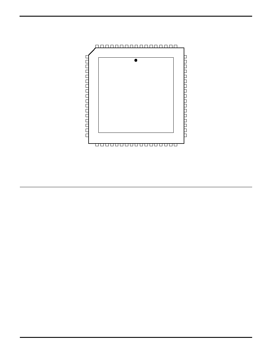
PIN DESCRIPTION
Figure 3. Z16C32 68-Pin PLCC Pin Assignments
Figure 2 shows the logical pin groupings of the IUSC's
pins, and Figure 3 shows the physical pin assignments.
Only one strobe pin (/DS, /RD, /WR or Pulsed INTACK)
should ever be active at one time. Any unused input pin (if
an input when the IUSC is bus master or slave) must be
pulled up to its inactive state.
/RESET
Reset (input, active Low). A Low on this line
places the IUSC in a known, inactive state, and conditions
it so that the data, from the next write operation that asserts
the /CS pin, goes into the Bus Configuration Register
(BCR) regardless of register addressing. /RESET should
be driven Low as soon as possible during power-up, and
as needed when restarting the overall system or the
communications subsystem.
CLK
System Clock (input). This signal is the timing refer-
ence for the DMA and bus interface logic. (The serial
controller section is clocked by the selected sources of
receive and transmit clocking.)
AD15-0
Address/Data Bus (inputs/tri-state outputs). After
Reset, these lines carry data between the controlling
microprocessor and the IUSC, and may also carry multi-
plexed addresses of registers within the IUSC. Such op-
eration, between the host processor and the IUSC, is often
called slave mode. Once the software has set up the
device and placed it into operation, these lines also carry
multiplexed addresses and data between the IUSC and
system memory; such operation is called master mode.
AD15-0 can be used in a variety of ways based on whether
the IUSC senses activity on /AS after Reset, and on the
data written to the Bus Configuration Register (BCR).
/CS
Chip Select (input, active Low). A Low on this line
indicates that the controlling microprocessor's current bus
cycle refers to a register in the IUSC. The IUSC ignores /CS
when a Low on /INTACK indicates that the current bus
operation is an interrupt acknowledge cycle. On a multi-
plexed bus the IUSC latches the state of this pin at rising
edges on /AS; on a non-multiplexed bus, it latches /CS at
leading/falling edges on /DS, /RD, or /WR.