CP97HHS0100
P R E L I M I N A R Y
1-1
1
P
RELIMINARY
C
USTOMER
P
ROCUREMENT
S
PECIFICATION
Z16C32 SL1660 O
NLY
1
IUSC
TM
I
NTEGRATED
U
NIVERSAL
S
ERIAL
C
ONTROLLER
GENERAL DESCRIPTION
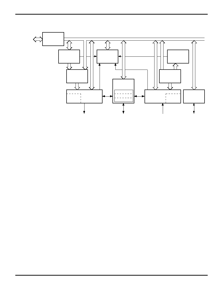
The IUSC (Integrated Universal Serial Controller) is a sin-
gle-channel multple protocol data communications device
with on-chip dual-channel DMA. The integration of a high-
speed serial communications channel with a high perfor-
mance DMA facilitates higher data throughput than is pos-
sible with discrete serial/DMA chip combinations. The buff-
er chaining capabilities combined with features like
character counters, frame status block and buffer termina-
tion at the end of the frame facilitate sophisticated buffer
management that can significantly reduce CPU overhead.
The IUSC is software configurable to satisfy a wide variety
of serial communications applications. Offered at 20
Mbit/sec, its fast data transfer rate and multiple protocol
support make it ideal for applications in todays dynamic
environment of changing specifications and ever increas-
ing speed. The many programmable features allow the
user to tune the device response to meet system require-
ments and adapt to future changes with software instead
of redesigning hardware.
The on-chip DMA channels allow high-speed data trans-
fers for both the receiver and the transmitter. The device
supports automatic status transfer through DMA and al-
lows device initialization under DMA control. Each DMA
channel can transfer data words in as little as three 50 ns
clock cycles and can generate addresses compatible with
32-, 24- or 16-bit memory ranges. The DMA channels may
operate in any of four modes: single buffer, pipelined, ar-
ray-chained, or linked-list. The array-chained and linked-
list modes reduce the problems with segmentation and re-
assembly of messages in systems. To prevent the DMA
from holding bus mastership too long, mastership time
may be limited by counting the absolute number of clock
cycles, the number of bus transactions, or both.
The CPU bus interface is designed for use with any con-
ventional multiplexed or non-multiplexed bus. The device
contains a variety of sophisticated internal functions includ-
ing two baud rate generators, a digital phase-locked loop,
character counters, and 32-byte FIFOs for both the receiv-
er and transmitter.
The IUSC handles asynchronous formats, synchronous
byte-oriented formats (e.g., BISYNC), and synchronous
bit-oriented formats such as HDLC. This device supports
virtually any serial data transfer application.
The IUSC can generate, and check CRC in any synchro-
nous mode and is programmed to check data integrity in
various modes. Access to the CRC value allows system
software to resend or manipulate it as needed in various
applications. The IUSC also has facilities for modem con-
trols. In applications where these controls are not needed,
the modem controls can be used for general-purpose I/O.
Interrupts are supported by a daisy-chain hierarchy within
the serial channel and between the serial channel and the
DMA.
Support tools are available to aid the designer in efficiently
programming the IUSC. The Technical Manual describes
in detail all features presented in this Product Specification
and gives programming sequence hints. The EPM
TM
man-
ual (Electronic Programmers Manual) is an MS-DOS, disk-
based programming initialization tool, used in conjunction
with the Technical Manual. Also, there are assorted appli-
cation notes and development boards to assist the design-
er in hardware/software development.
Notes:
All signals with a preceding front slash, "/", are
active Low. For example, B//W (WORD is active Low);
/B/W (BYTE is active Low, only).
Power connections follow conventional descriptions
below:
Connection
Circuit
Device
Power
V
CC
V
DD
Ground
GND
V
SS