
1
P R E L I M I N A R Y
Z80185/Z80195
S
MART
P
ERIPHERAL
C
ONTROLLES
DS971850301
Zilog
P
RELIMINARY
P
RODUCT
S
PECIFICATION
Z80185/Z80195
S
MART
P
ERIPHERAL
C
ONTROLLERS
FEATURES
s
Enhanced Z8S180 MPU
s
Four Z80
CTC Channels
s
One Channel ESCC
TM
Controller
s
Two 8-Bit Parallel I/O Ports
s
Bidirectional Centronics Interface (IEEE 1284)
s
Low-EMI Option
ROM
UART
Speed
Part
(KB)
Baud Rate
(MHz)
Z80185
32 x 8
512 Kbps
20, 33
Z80195
0
512 Kbps
20, 33
s
100-Pin QFP Package
s
5.0-Volt Operating Range
s
Low-Power Consumption
s
0
∞
C to +70
∞
C Temperature Range
GENERAL DESCRIPTION
The Z80185 and Z80195 are smart peripheral controller
devices designed for general data communications appli-
cations, and architected specifically to accommodate all
input and output (I/O) requirements for serial and parallel
connectivity. Combining a high-performance CPU core
with a variety of system and I/O resources, the Z80185/195
are useful in a broad range of applications. The Z80195 is
the ROMless version of the device.
The Z80185 and Z80195 feature an enhanced Z8S180
microprocessor linked with one enhanced channel of the
Z85230 ESCC
TM
serial communications controller, and 25
bits of parallel I/O, allowing software code compatibility
with existing software code.
Seventeen lines can be configured as bidirectional
Centronics (IEEE 1284) controllers. When configured as a
1284 controller, an I/O line can operate in either the host or
peripheral role in compatible, nibble, byte or ECP mode. In
addition, the Z80185 includes 32 Kbytes of on-chip ROM.
These devices are well-suited for external modems using
a parallel interface, protocol translators, and cost-effective
WAN adapters. The Z80185/195 is ideal for handling all
laser printer I/O, as well as the main processor in cost-
effective printer applications.
Notes:
All Signals with a preceding front slash, "/", are active Low.
Power connections follow conventional descriptions below:
Connection
Circuit
Device
Power
V
CC
V
DD
Ground
GND
V
SS

2
P R E L I M I N A R Y
Z80185/Z80195
S
MART
P
ERIPHERAL
C
ONTROLLERS
DS971850301
Zilog
Processor
Power Controller
Parallel Ports (2)
Including IEEE
Bidirectional
Centronics Controller
16-Bit Programmable
Reload Timers (2)
UARTs (2)
ROM
32K x 8
(Z80185 Only)
DMACs (2)
EMSCC
Decode
CTCs (4)
16-Bit Address Bus
8-Bit Data Bus
/ROMCS
/RAMCS
MMU
A19-0
TxD,
RxD
TOUT
CLK/TRG
ZC/TO
TXA1-0,
RXA1-0
TIMING DIAGRAMS
(Continued)
Figure 1. Z80185/195 Functional Block Diagram
3
P R E L I M I N A R Y
Z80185/Z80195
S
MART
P
ERIPHERAL
C
ONTROLLES
DS971850301
Zilog
/BUSREQ
/BUSACK
NSTROBE
NACK
NAUTOFD
TOUT//DREQ
BUSY
NINIT
RXA1
/INT0
/NMI
/RESET
/W
AIT
EXT
AL
VSS
A17
PHI
/RD
/WR
/M1
NF
AUL
T
/MREQ
/IORQ
XT
AL
/RFSH
VDD
/HAL
T
Z80185/Z80195
100-Pin QFP
/INT1
/INT2
ST
A0
A1
A2
A3
A15
A4
A5
A6
A7
A8
A9
A11
A12
VSS
A13
A14
A16
D0
D1
D2
D3
D4
D5
D7
/RAMCS
/IOCS
TXA1
CKA0/CKS
RXA0
TXA0
/DCD0/CKA1
/CTS0/RXS
/RTS0/TXS
A18
A19
VSS
IEI
/ROMCS
IEO
VSS
/DCD
/CTS
/RTS
/DTR
TXD
/TRXC
RXD
PERROR
100
1
95
5
10
15
90
85
80
75
70
65
60
55
50
45
40
35
30
25
20
D6
A10
PIA10/CLKTRG0
PIA1
1/CLKTRG1
PIA12/CLKTRG2
PIA13/CLKTRG3
PIA14/ZCT
O0
PIA15/ZCT
O1
PIA16/ZCT
O2
SELECT
VSS
PIA21
PIA22
PIA23
PIA24
PIA25
PIA26
PIA27
/R
TXC
NSELECTIN
PIA20
VDD
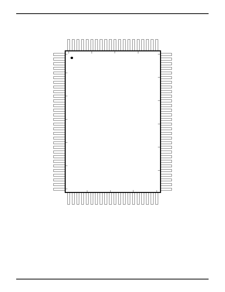
PIN DESCRIPTION
Figure 2. 100-Pin QFP Pin Assignments

4
P R E L I M I N A R Y
Z80185/Z80195
S
MART
P
ERIPHERAL
C
ONTROLLERS
DS971850301
Zilog
1.4 V
I
OH
100 pF
OL
I
= 2 mA
= 250
µ
A
ABSOLUTE MAXIMUM RATINGS
Symbol Description
Min
Max
Units
V
CC
Supply Voltage
≠0.3
+7.0
V
V
IN
Input Voltage
≠0.3
V
CC
+0.3
V
T
OPR
Operating Temp.
0
70
∞
C
T
STG
Storage Temp.
≠55
+150
∞
C
Notes:
Voltage on all pins with respect to GND. Permanent LSI damage may
occur if maximum ratings are exceeded. Normal operation should be
recommended operating conditions. If these conditions are exceeded, it
could affect reliability of LSI.
Stresses greater than those listed under Absolute Maxi-
mum Ratings may cause permanent damage to the de-
vice. This is a stress rating only; operation of the device at
any condition above those indicated in the operational
sections of these specifications is not implied. Exposure to
absolute maximum rating conditions for extended periods
may affect device reliability.
STANDARD TEST CONDITIONS
The DC Characteristics and capacitance sections below
apply for the following standard test conditions, unless
otherwise noted. All voltages are referenced to GND (0V).
Positive current flows into the referenced pin (Test Load).
Operating Temperature Range:
S = 0
∞
C to 70
∞
C
Voltage Supply Range:
+4.5V
V
CC
+5.5V
All AC parameters assume a load capacitance of 100 pF.
Add 10 ns delay for each 50 pF increase in load up to a
maximum of 150 pF for the data bus and 100 pF for
address and control lines. AC timing measurements are
referenced to 1.5 volts (except for clock, which is refer-
enced to the 10% and 90% points). Maximum capacitive
load for PHI is 125 pF.
Figure 3. Test Load Diagram

5
P R E L I M I N A R Y
Z80185/Z80195
S
MART
P
ERIPHERAL
C
ONTROLLES
DS971850301
Zilog
DC CHARACTERISTICS
V
DD
= 5.0V
±
10%, V
SS
= 0V over specified temperature range, unless otherwise noted.
Symbol
Item
Condition
Min.
Typ.
Max.
Unit
V
IH
Input "H" Voltage
V
V
IL
Input "L" Voltage
V
V
OH
Output "H" Voltage
V
V
OL1
Output "L" Voltage
V
I
IL
Input Leakage
V
IN
=0.5 to
Current All Inputs
V
DD
≠0.5
1.0
Except XTAL,EXTAL
µ
A
I
TL
Tri-State Leakage
V
IN
=0.5 to
Current
V
DD
≠0.5
1.0
µ
A
V
DD
Supply Current*
Normal Operation
For 5.0V:
f = 20 MHz
60
120
mA
For 5.0V:
f = 33 MHz
68
132
mA
I
CC
*
Power Dissipation*
System Stop Mode
For 5.0V:
f = 20 MHz
5
10
mA
For 5.0V:
f = 33 MHz
7
13
mA
Notes:
See Class Reference Table
* V
IH
min = V
DD
≠1.0V, V
IL
max = 0.8V (All output terminals are at no load.)
6
P R E L I M I N A R Y
Z80185/Z80195
S
MART
P
ERIPHERAL
C
ONTROLLERS
DS971850301
Zilog
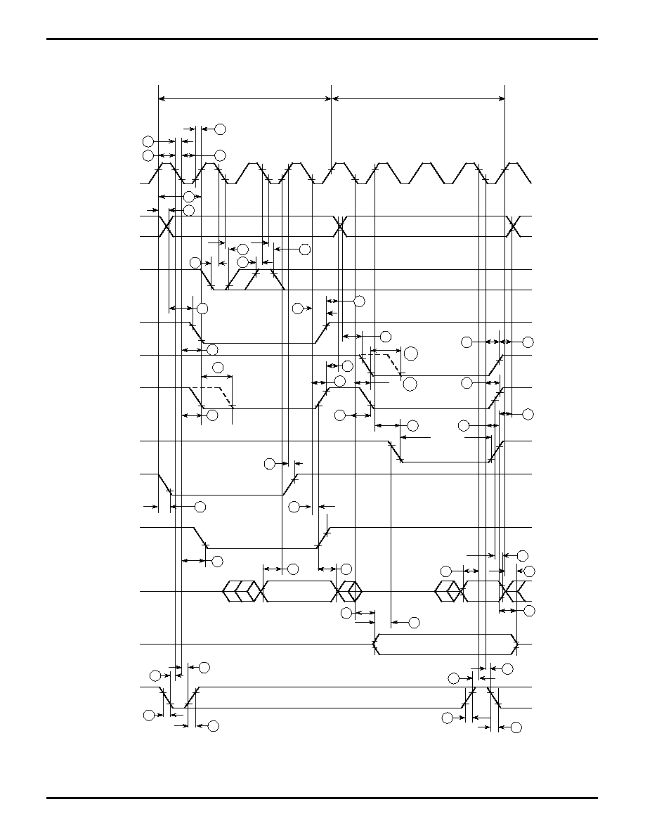
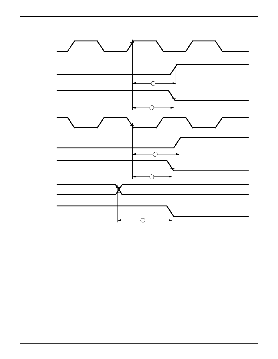
TIMING DIAGRAMS
Z8S180 MPU Timing
Figure 4. CPU Timing
(Opcode Fetch Cycle, Memory Read/Write Cycle
I/O Read/Write Cycle)
¯
Address
Opcode Fetch Cycle
T1
T2
TW
T3
T1
T2
TW
T3
T1
I/O Write Cycle
I/O Read Cycle
/WAIT
/MREQ
6
1
3
2
4
5
19
20
19
20
7
8
12
11
7
11
29
/IORQ
13
11
13
9
/RD
/WR
22
26 and 26a
25
11
10
14
18
/M1
17
ST
Data
IN
Data
OUT
/RESET
15
16
15
16
27
21
23
24
48
49
54
53
48
49
54
53
28a
28b
9a
9b
7
P R E L I M I N A R Y
Z80185/Z80195
S
MART
P
ERIPHERAL
C
ONTROLLES
DS971850301
Zilog
ÿ
32
31
33
30
15
16
39
40
41
42
34
35
35
34
37
36
38
38
43
[3]
/INTI
/NMI
/M1 [1]
/IORQ [1]
/Data IN [1]
/MREQ [2]
/RFSH [2]
/BUSREQ
/BUSACK
Address
Data /MREQ,
/RD, /WR,
/IORQ
/HALT
44
Notes:
[1] During /INT0 acknowledge cycle
[2] During refresh cycle
[3] Output buffer is off at this point
[4] Refer to Table C, parameter 7
Figure 5. CPU Timing
(/INT0 Acknowledge Cycle, Refresh Cycle, BUS RELEASE mode
HALT mode, SLEEP mode, SYSTEM STOP mode)
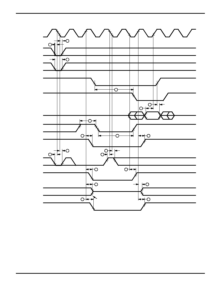
TIMING DIAGRAMS
(Continued)

8
P R E L I M I N A R Y
Z80185/Z80195
S
MART
P
ERIPHERAL
C
ONTROLLERS
DS971850301
Zilog
0
Address
/IROQ
T1
T2
TW
T3
T1
13
25
9
/RD
/WR
T2
TW
T3
I/O Read Cycle
I/O Write Cycle
28
29
28
29
22
ÿ
45
46
45
45
17
18
CPU or DMA Read/Write Cycle
T1
T2
Tw
T3
T1
[3]
[4]
[2]
[1]
TOUT//DREQ
(At level
sense)
TOUT//DREQ
(At edge
sence)
ST
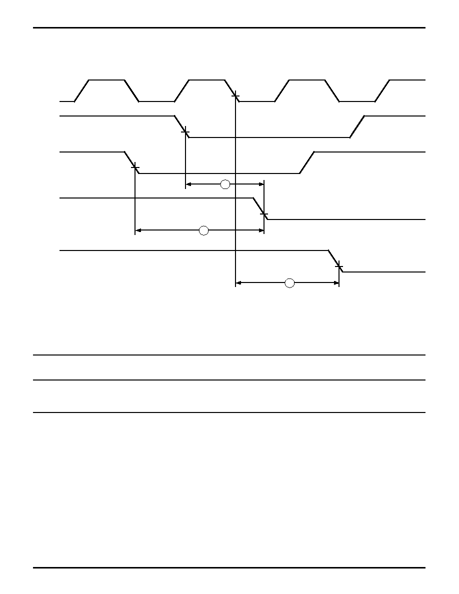
DMA Control Signals
[1] tDRQS and tDRQH are specified for the rising edge of clock followed by T3.
[2] tDRQS and tDRQH are specified for the rising edge of clock.
[3] DMA cycle starts.
[4] CPU cycle starts.
Figure 6. CPU Timing
Figure 7. DMA Control Signals
9
P R E L I M I N A R Y
Z80185/Z80195
S
MART
P
ERIPHERAL
C
ONTROLLES
DS971850301
Zilog
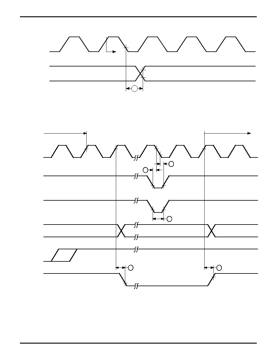
ÿ
47
TOUT/DREQ
Timer Data
Reg = 0000H
ÿ
T3
T1
T2
TS
TS
T1
T2
32
31
33
43
44
/INTi
/NMI
A18-A0
/MREQ, /M1
/RD
/HALT
SLP Instruction Fetch
Next Opcode Fetch
TIMING DIAGRAMS
(Continued)
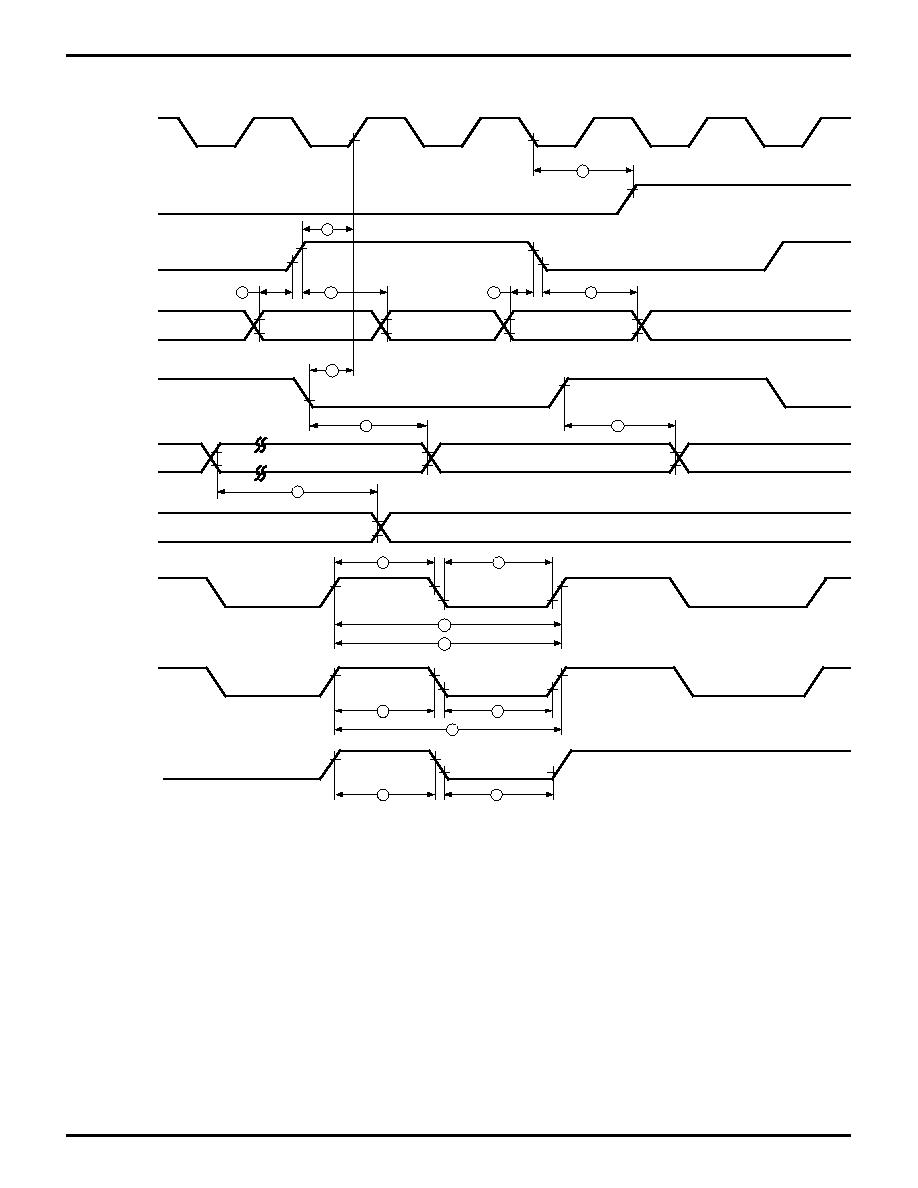
Figure 9. SLEEP Execution Cycle
Figure 8. Timer Output Timing
10
P R E L I M I N A R Y
Z80185/Z80195
S
MART
P
ERIPHERAL
C
ONTROLLERS
DS971850301
Zilog
CSI/O Clock
58
58
60
59
60
59
62
61
61
62
11.5 tcyc
11 tcyc
11 tcyc
11.5 tcyc
16.5 tcyc
16.5 tcyc
57
57
Transmit Data
(Internal Clock)
Transmit Data
(External Clock)
Receive Data
(Internal Clock)
Receive Data
(External Clock)
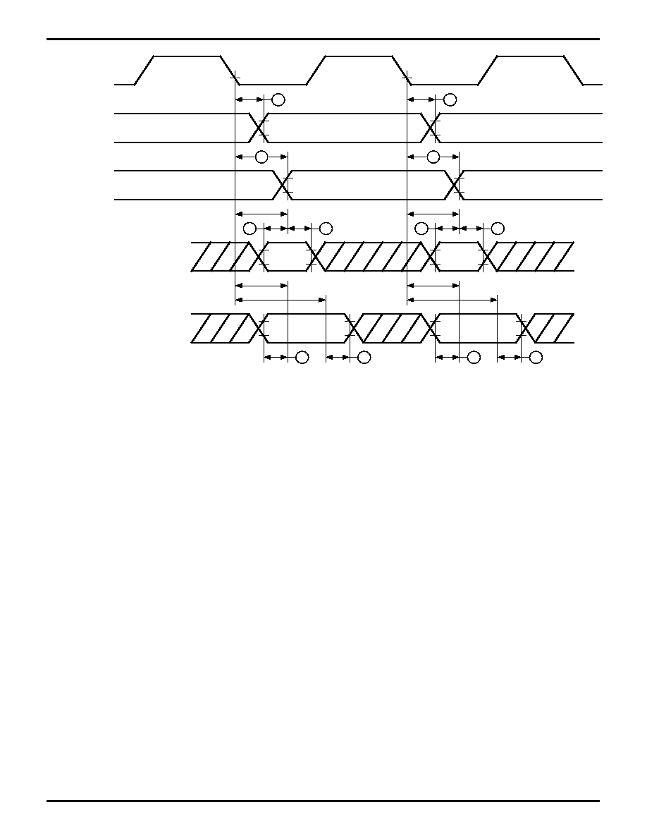
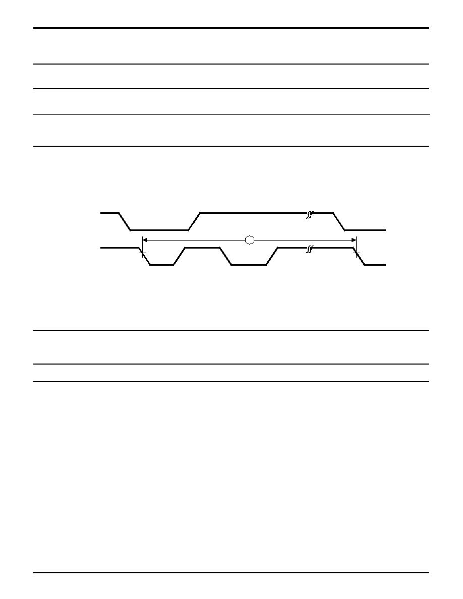
Figure 10. CSI/O Receive/Transmit Timing
11
P R E L I M I N A R Y
Z80185/Z80195
S
MART
P
ERIPHERAL
C
ONTROLLES
DS971850301
Zilog
/MREQ
63
64
/RAMCS
/ROMCS
/IORQ
/IOCS
56
55
EXTAL
VIL1
51
52
VIH1
VIL1
VIH1
TIMING DIAGRAMS
(Continued)
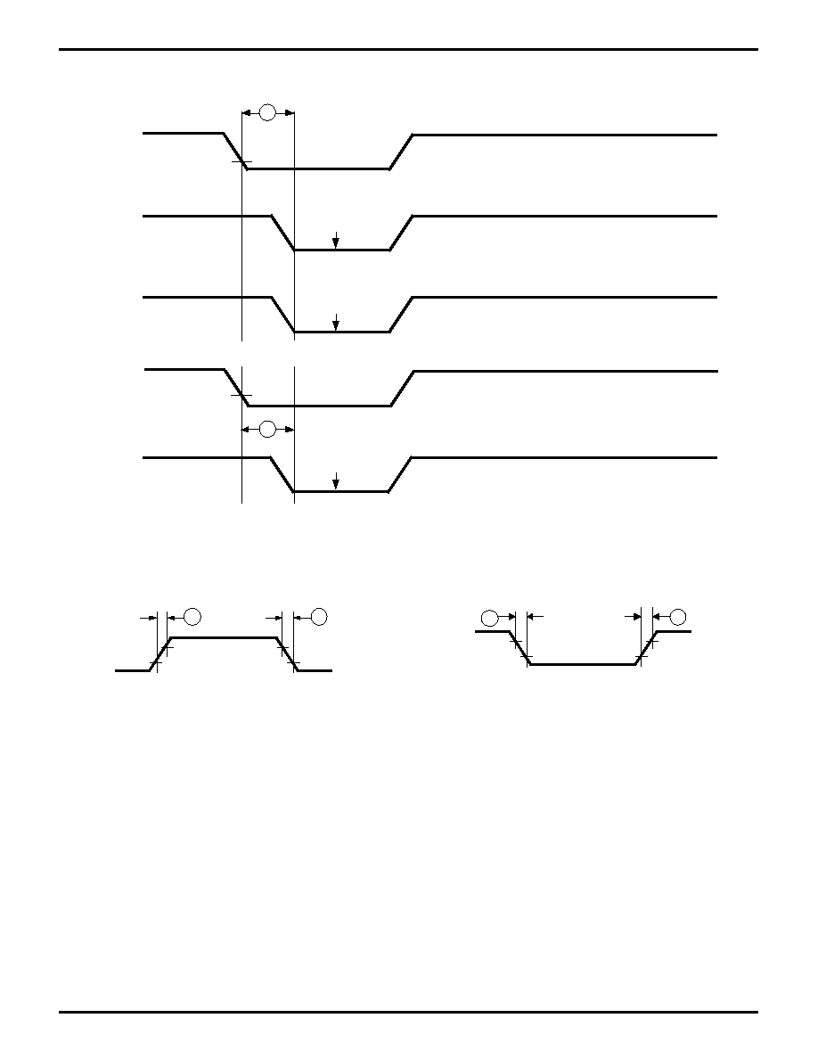
Figure 11. /ROMCS and /RAMCS Timing
Figure 12. External Clock Rise Time
and Fall Time
Figure 13. Input Rise and Fall Time
(Except EXTAL, /RESET)

12
P R E L I M I N A R Y
Z80185/Z80195
S
MART
P
ERIPHERAL
C
ONTROLLERS
DS971850301
Zilog
AC CHARACTERISTICS
V
DD
= 5V
±
10%, V
SS
= 0V, CL = 50 pF for outputs over
specified temperature range, unless otherwise noted.
Z80185 / Z80195
Z80185 / Z80195
(20 MHz)
(33 MHz)
No.
Symbol Parameter
Min
Max
Min
Max
Units
1
tcy
Clock Cycle Time
50
(DC)
33
(DC)
ns
2
tCHW
Clock "H" Pulse Width
15
10
ns
3
tCLW
Clock "L" Pulse Width
15
10
ns
4
tcf
Clock Fall Time
10
5
ns
5
tcr
Clock Rise Time
10
5
ns
6
tAD
PHI Rising to Address Valid
30
15
ns
7
tAS
Address Valid to (MREQ Falling or IORQ Falling)
5
5
ns
8
tMED1
PHI Falling to MREQ Falling Delay
25
15
ns
9a
tRDD1
PHI Falling to RD Falling Delay (IOC=1)
25
15
ns
9b
tRDD1
PHI Rising to RD Falling Delay (IOC=0)
25
15
ns
10
tM1D1
PHI Rising to M1 Falling Delay
35
15
ns
11
tAH
Address Hold Time from (MREQ, IOREQ, RD, WR)
5
5
ns
12
tMED2
PHI Falling to MREQ Rising Delay
25
15
ns
13
tRDD2
PHI Falling to RD Rising Delay
25
15
ns
14
tM1D2
PHI Rising to M1 Rising Delay
40
15
ns
15
tDRS
Data Read Setup Time
10
5
ns
16
tDRH
Data Read Hold Time
0
0
ns
17
tSTD1
PHI Falling to ST Falling Delay
30
15
ns
18
tSTD2
PHI Falling to ST Rising Delay
30
15
ns
19
tWS
WAIT Setup Time to PHI Falling
15
10
ns
20
tWH
WAIT Hold Time from PHI Falling
10
5
ns
21
tWDZ
PHI Rising to Data Float Display
35
20
ns
22
tWRD1
PHI Rising to WR Falling Delay
25
15
ns
23
tWDD
PHI Rising to Write Data Delay Time
25
15
ns
24
tWDS
Write Data Setup Time to WR Falling
10
10
ns
25
tWRD2
PHI Falling to WR Rising Delay
25
15
ns
26
tWRP
Write Pulse Width (Memory Write Cycle)
75
45
ns
26a
tWRP
Write Pulse Width (I/O Write Cycle)
130
70
ns
27
WDH
Write Data Hold Time From (WR Rising)
10
5
ns
Notes:
Specifications 1 through 5 refer to an external clock input on EXTAL, and
provisionally to PHI clock output. When a quartz crystal is used with the
on-chip oscillator, a lower maximum frequency than that implied by spec.
#1 may apply.

13
P R E L I M I N A R Y
Z80185/Z80195
S
MART
P
ERIPHERAL
C
ONTROLLES
DS971850301
Zilog
AC CHARACTERISTICS
(Continued)
Z80185 / Z80195
Z80185 / Z80195
(20 MHz)
(33 MHz)
No.
Symbol Parameter
Min
Max
Min
Max
Units
28a
tIOD
PHI Falling to IORQ Falling Delay IOC = 1)
25
15
ns
28b
tIOD
PHI Rising to IORQ Fallin g Delay (IOC =0)
25
15
ns
29
tIOD2
PHI Falling to IORQ Rising Delay
25
15
ns
30
tIOD3
M1 Falling to IORQ Falling Delay
100
80
ns
31
tINTS
INT Setup Time to PHI Falling
20
15
ns
32
tINTH
INT Hold Time from PHI Falling
10
10
ns
33
tNMIW
NMI Pulse Width
35
25
ns
34
tBRS
BUSREQ Setup Time to PHI Falling
10
10
ns
35
tBRH
BUSREQ Hold Time from PHI Falling
10
10
ns
36
tBAD1
PHI Rising to BUSACK Falling Delay
25
15
ns
37
tBAD2
PHI Falling to BUSACK Rising Delay
25
15
ns
38
tBZD
PHI Rising to Bus Floating Delay Time
40
30
ns
39
tMEWH
MREQ Pulse Width (High)
tcy ≠15
tcy ≠10
ns
40
tMEWL
MREQ Pulse Width (Low)
2tcy ≠15
2tcy≠10
ns
41
tRFD1
PHI Rising to RFSH Falling Delay
20
15
ns
42
tRFD2
PHI Rising to RFSH Rising Delay
20
15
ns
43
tHAD1
PHI Rising to HALT Falling Delay
15
15
ns
44
tHAD2
PHI Rising to HALT Rising Delay
15
15
ns
45
tDRQS
DREQ Setup Time to PHI Rising
20
15
ns
46
tDRQH
DREQ Hold Time from PHI Rising
20
15
ns
47
tTOD
PHI Falling to Timer Output Delay
75
50
ns
48
tRES
RESET Setup Time to PHI Falling
40
25
ns
49
tREH
RESET Hold Time From PHI Falling
25
15
ns
50
tOSC
Oscillator Stabilization Time
20
20
ms
51
tEXr
External Clock Rise Time (EXTAL)
10
5
ns
52
tEXf
External Clock Fall Time (EXTAL)
10
5
ns
53
tRr
Reset Rise Time
50
50
ms
54
tRf
Reset Fall Time
50
50
ms
55
tIr
Input Rise Time (Except EXTAL, RESET)
50
50
ns
56
tIf
Input Fall Time (Except EXTAL, RESET)
50
50
ns
57
tSTDI
CSIO Transmit Data Delay Time
75
60
ns
(Internal Clock Operation)
58
tSTDE
CSIO Transmit Data Delay Time
7.5 tcy +75
7.5 tcy +60
ns
(External Clock Operation)
59
tSRSI
CSIO Receive Data Setup Time
75
60
ns
(Internal Clock Operation)
60
tSRHI
CSIO Receive Data Hold Time
75
60
ns
(Internal Clock Operation)
61
tSRSE
CSIO Receive Data Setup Time
75
60
ns
(External Clock Operation)
62
tSRHE
CSIO Receive Data Hold Time
75
60
ns
(External Clock Operation)
63
tdCS
MREQ Valid to RAMCS and ROMCS Valid Delay
15
15
ns
64
tdIOCS
Rising IORQ Valid to Rising IOCS Valid Delay
10
10
ns

14
P R E L I M I N A R Y
Z80185/Z80195
S
MART
P
ERIPHERAL
C
ONTROLLERS
DS971850301
Zilog
Address
B5
B7
B3
Data In
Data Out
A7-A0
/IORQ
/RD
Data
/WR
Data
B6
B2
B2
B4
B9
B1
B8
AC CHARACTERISTICS
(Continued)
Read/Write External Bus Master Timing
Figure 14. Read/Write External Bus Master Timing

15
P R E L I M I N A R Y
Z80185/Z80195
S
MART
P
ERIPHERAL
C
ONTROLLES
DS971850301
Zilog
AC CHARACTERISTICS
(Continued)
General-Purpose I/O Timing Port Timing
Parameters referenced in Figure 15 appear in the following
Tables.
Note:
Port 2 timing is different, even when Bidirec-
tional Centronics feature is not in active use.
Figure 15. PORT Timing
T1
T2
TW
T3
T1
T2
TW
T3
T1
T2
TW
T3
0
A0-A7
/IORQ
D0-D7
/WR
Port
I/O Port Timing
(Output)
Port (Output)
Port Output Data 1 (Out)
Port Output Data 2 (In)
Port Output Data 1
(In)
(In) 'OO'H (Change Port To
Output)
Port Data Dir. Reg. Addr. (Input)
Port Data Reg. Addr. (Input)
Port Data Reg. Addr. (Input)
B7
B7
B7
B2
B3
B2
B3
B2
B6
B6
B6
A1
A1
A2
A0-A7
/IORQ
D0-D7
/WR
/RD
Port
Previous
Output
Port Input Data
1 (In)
Port Input Data
2 (In)
Port Data
2 Out
Port Data 1 (Out)
(In) 'FF'H (Change
Port To Input)
Port Data Dir. Reg.
Addr. (Input)
Port Data Reg.
Addr. (Input)
Port Data Reg.
I/O Port Timing (Input)
B4
B2
B4
B2

16
P R E L I M I N A R Y
Z80185/Z80195
S
MART
P
ERIPHERAL
C
ONTROLLERS
DS971850301
Zilog
I/O Port Timing
Z80185 / Z80195
Z80185 / Z80195
(20 MHz)
(33 MHz)
No.
Symbol
Parameter
Min
Max
Min
Max
Units
A1
TdWR (PIA)
Data Valid Delay from WR Rise
60
60
ns
External Bus Master Timing
Z80185 / Z80195
Z80185 / Z80195
(20 MHz)
(33 MHz)
No.
Symbol
Parameter
Min
Max
Min
Max
Units
B1
TsA(wf)
Address Valid to WR or
(rf)
RD Fall Time
40
40
ns
B2
TsIO(wf)
IORQ Fall to WR or
(rf)
RD Fall Time
20
20
ns
B3
Th
Data Hold Time (from WR Rise)
5
5
ns
B4
TdRD(DO)
RD Fall to Data Out Delay
35
35
ns
B5
TdRIr(DOz)
RD,IORQ Rise to Data Float Time
5
5
ns
B6
TsDI(WRf)
Data In to WR Fall Setup Time
20
20
ns
B7
TsA(IORQf)
Address to IORQ Fall Setup Time
20
20
ns
B8
TsA(RDf)
Address to RD Fall Setup Time
40
40
ns
B9
TsA(WRf)
Address to WR Fall Setup Time
40
40
ns
17
P R E L I M I N A R Y
Z80185/Z80195
S
MART
P
ERIPHERAL
C
ONTROLLES
DS971850301
Zilog
ÿ
2
6
1
/WR
/RD
Wait
/INT
AC CHARACTERISTICS
(Continued)
EMSCC Timing
Figure 16. EMSCC AC Parameters
EMSCC Timing Parameters
20 MHz
No.
Symbol
Parameter
Min
Max
Unit
1
TdWR(W)
/WR Fall to Wait Valid Delay
50
ns
2
TdRD(W)
/RD Fall to Wait Valid Delay
50
6
TdPC(INT)
Clock to /INT Valid Delay
160
18
P R E L I M I N A R Y
Z80185/Z80195
S
MART
P
ERIPHERAL
C
ONTROLLERS
DS971850301
Zilog
PCLK
Wait
/RTxC, /TRxC
Receive
RxD
/TRxC, /RTxC
Transmit
TxD
/TRxC
Output
/RTxC
/TRxC
/CTS, /DCD
2
3
4
5
6
7
10
11
12
13
14
15
16
17
18
19
20
21
21
EMSCC General Timing Diagram
Figure 17. EMSCC General Timing Diagram

19
P R E L I M I N A R Y
Z80185/Z80195
S
MART
P
ERIPHERAL
C
ONTROLLES
DS971850301
Zilog
AC CHARACTERISTICS
(Continued)
EMSCC General Timing
20 MHz
No.
Symbol
Parameter
Min
Max
Notes
2
TdPC(W)
/PCLK to Wait Inactive
170
3
TsRxC(PC)
/RxC to /PCLK Setup Time
NA
[1,4]
4
TsRxD(RxCr)
RxD to /RxC Setup Time
0
[1]
5
ThRxD(RxCr)
RxD to /RxC Hold Time
45
[1]
6
TsRxD(RxCf)
RxD to /RxC Setup Time
0
[1,5]
7
ThRxD(RxCf)
RxD to /RxC Hold Time
45
[1,5]
10
TsTxC(PC)
/TxC to /PCLK Setup Time
NA
[2,4]
11
TdTxCf(TXD)
/TxC to TxD Delay
70
[2]
12
TdTxCr(TXD)
/TxC to TxD Delay
70
[2,5]
13
TdTxD(TRX)
TxD to TRxC Delay
80
70
14
TwRTxh
RTxC High Width
70
[6]
15
TwRTxI
TRxC Low Width
70
[6]
16a
TcRTx
RTxC Cycle Time
200
[6,7]
16b
TxRx(DPLL)
DPLL Cycle Time Min
50
[7,8]
17
TcRTxx
Crystal OSC. Period
61
1000
[3]
18
TwTRxh
TRxC High Width
70
[6]
19
TwTRxl
TRxC Low Width
70
[6]
20
TcTRx
TRxC Cycle Time
200
[6,7]
21
TwExT
DCD or CTS Pulse Width
60
Notes:
[1] RxC is /RTxC or /TRxC, whichever is supplying the receive clock.
[2] TxC is /TRxC or /RTxC, whichever is supplying the transmit clock.
[3] Both /RTxC and /SYNC have 30 pF capacitors to Ground connected to them.
[4] Synchronization of RxC to PCLK is eliminated in divide-by-four operation.
[5] Parameter applies only to FM encoding/decoding.
[6] Parameter applies only for transmitter and receiver; DPLL and baud
rate generator timing requirements are identical to case PCLK requirements.
[7] The maximum receive or transmit data rate is 1/4 PCLK.
[8] Applies to DPLL clock source only. Maximum data rate of 1/4 PCLK
still applies. DPLL clock should have a 50% duty cycle.
These AC parameter values are preliminary and subject to change without notice.
20
P R E L I M I N A R Y
Z80185/Z80195
S
MART
P
ERIPHERAL
C
ONTROLLERS
DS971850301
Zilog
2
4
10
8
6
/RTxC, /TRxC
Receive
/W/REQ
Wait
/INT
/RTxC, /TRxC
Transmit
Wait
/INT
/CTS,
/DCD
/INT
EMSCC System Timing Diagram
Figure 18. EMSCC System Timing
21
P R E L I M I N A R Y
Z80185/Z80195
S
MART
P
ERIPHERAL
C
ONTROLLES
DS971850301
Zilog
1
Valid ESCC
Addr * IORQ
/RD or
/WR
AC CHARACTERISTICS
(Continued)
EMSCC System Timing
20 MHz
No.
Symbol
Parameter
Min
Max
Notes
2
TdRxC(W)
/RxC to /Wait Inactive
13
18
[1,2]
4
TdRxC(INT)
/RxC to /INT Valid
15
22
[1,2]
6
TdTxC(W)
/TxC to /Wait Inactive
8
17
[1,3]
8
TdTxC(INT)
/TxC to /INT Valid
9
17
[1,3]
10
TdExT(INT)
/DCD or /CTS to /INT Valid
3
9
[1]
Notes:
[1] Open-drain output, measured with open-drain test load.
[2] /RxC is /RTxC or /TRxC, whichever is supplying the receive clock.
Figure 19. EMSCC External Bus Master Timing
External Bus Master Interface Timing
(SCC Related Timing)
Z80185 / Z80195
Z80185 / Z80195
(20 MHz)
(33 MHz)
No
Symbol
Parameter
Min
Max
Min
Max
Unit
Notes
1
TrC
Valid Access Recovery Time
4TcC
4TcC
ns
[1]
Notes:
[1] Applies only between transactions involving the EMSCC.
These AC parameter values are preliminary and subject to change
without notice.
T
CC
= EMSCC Clock Period Time
[3] /TxC is /TRxC or /RTxC, whichever is supplying the transmit clock.
[4] Units equal to TcPc
These AC parameter values are preliminary and subject to change
without notice.

22
P R E L I M I N A R Y
Z80185/Z80195
S
MART
P
ERIPHERAL
C
ONTROLLERS
DS971850301
Zilog
1
Port 2
Output
2
4
3
6
5
Control
Output
Control
Input
Port 2
Input
AC CHARACTERISTICS
(Continued)
Figure 20. P1284 Bidirectional Centronics Interface Timing
P1284 Bidirectional Centronics Interface Timing
No.
Parameter
Min
Max
Units
Notes
1
CLK High to Port 2 Output
12
ns
2
CLK High to Control Output
12
ns
[1]
3
Setup Time for Control Input to
CLK High for Guaranteed Recognition
10
ns
[2]
4
Hold Time for Control Input from
CLK High for Guaranteed Recognition
5
ns
[2]
5
Setup Time for Port 2 Inputs to
CLK High for Guaranteed Recognition
10
ns
6
Hold Time for Port 2 Inputs to
CLK High for Guaranteed Recognition
5
ns
Notes:
[1]
Control Outputs
Peripheral Mode
Host Mode
Busy/PtrBusy/PeriphAck
nStrobe/HostClk
nAck/PtrClk/PeriphClk
nAutoFd/HostBusy/HostAck
PError/AckDataReq/nAckReverse
nSelectIn/P1284Active
nFault/nDataAvail/nPeriphRequest
nInit/nReverseRequest
Select/Xflag
[2]
Control Inputs
Host Mode
Peripheral Mode
Busy/PtrBusy/PeriphAck
nStrobe/HostClk
nAck/PtrClk/PeriphClk
nAutoFd/HostBusy/HostAck
PError/AckDataReq/nAckReverse
nSelectIn/P1284Active
nFault/nDataAvail/nPeriphRequest
nInit/nReverseRequest
Select/Xflag

23
P R E L I M I N A R Y
Z80185/Z80195
S
MART
P
ERIPHERAL
C
ONTROLLES
DS971850301
Zilog
PIN DESCRIPTIONS
Z80185 CPU Signals
A0-A19.
Address Bus (input/output, active High, tri-state).
A0-A19 is a 20-bit address bus that provides the address
for memory data bus cycles up to 1 Mbyte, and I/O data
bus cycles up to 64 Kbytes. The address bus enters a High
impedance state during reset and external bus acknowl-
edge cycles. This bus is an input when /BUSACK is Low.
No address lines are multiplexed with any other signals.
D0-D7.
Data Bus (bidirectional, active High, tri-state). D0-
D7 constitute an 8-bit bidirectional data bus, used to
transfer information to and from I/O and memory devices.
The data bus enters the High impedance state during reset
and external bus acknowledge cycles, as well as during
SLEEP and HALT states.
/RD.
Read (input/output, active Low, tri-state). /RD indi-
cates that the CPU is ready to read data from memory or
an I/O device. The addressed I/O or memory device
should use this signal to gate data onto the CPU data bus.
This pin is tri-stated during bus acknowledge cycles.
/WR.
Write (input/output, active Low, tri-state). /WR indi-
cates that the CPU data bus holds valid data to be stored
at the addressed I/O or memory location. This pin is tri-
stated during bus acknowledge cycles.
/IORQ.
I/O Request (input/output, active Low, tri-state).
/IORQ indicates that the address bus contains a valid I/O
address for an I/O read or I/O write operation. /IORQ is also
generated, along with /M1, during the acknowledgment of
the /INT0 input signal to indicate that an interrupt response
vector can be placed onto the data bus. This pin is tri-
stated during bus acknowledge cycles.
/M1.
Machine Cycle 1 (input/output, active Low). Together
with /MREQ, /M1 indicates that the current cycle is the
opcode fetch cycle of an instruction execution. Together
with /IORQ, /M1 indicates that the current cycle is for an
interrupt acknowledge. It is also used with the /HALT and
ST signal to indicate the status of the CPU machine cycle.
The processor can be configured so that this signal is
compatible with the /M1 signal of the Z80, or with the /LIR
signal of the Z64180. This pin is tri-stated during bus
acknowledge cycles.
/MREQ.
Memory Request (input/output, active Low, tri-
state). /MREQ indicates that the address bus holds a valid
address for a memory read or memory write operation. It is
included in the /RAMCS and /ROMCS signals, and be-
cause of this may not be needed in some applications. This
pin is tri-stated during bus acknowledge cycles.
/WAIT.
(input/open-drain output, active Low.) /WAIT indi-
cates to the MPU that the addressed memory or I/O
devices are not ready for a data transfer. This input is used
to induce additional clock cycles into the current machine
cycle. External devices should also drive this pin in an
open-drain fashion. This results in a "wired OR" of the Wait
indications produced by external devices and those pro-
duced by the two separate Wait State generators in the
Z80185. If the wire-ORed input is sampled Low, then
additional wait states are inserted until the /WAIT input is
sampled High, at which time the cycle is completed.
/HALT.
Halt/Sleep Status (output, active Low). This output
is asserted after the CPU has executed either the HALT or
SLP instruction, and is waiting for either non-maskable or
maskable interrupt before operation can resume. It is also
used with the /M1 and /ST signals to indicate the status of
the CPU machine cycle. On exit of Halt/Sleep, the first
instruction fetch is delayed 16 clock cycles after the /HALT
pin goes High.
/BUSACK.
Bus Acknowledge (output, active Low).
/BUSACK indicates to the requesting device that the MPU
address and data bus, as well as some control signals,
have entered their High impedance state.
/BUSREQ.
Bus Request (input, active Low). This input is
used by external devices (such as DMA controllers) to
request access to the system bus. This request has a
higher priority than /NMI and is always recognized at the
end of the current machine cycle. This signal stops the
CPU from executing further instructions and places the
address and data buses, and other control signals, into the
High impedance state.
/NMI.
Non-Maskable Interrupt (input, negative edge trig-
gered). /NMI has a higher priority than /INT and is always
recognized at the end of an instruction, regardless of the
state of the interrupt enable flip-flops. This signal forces
CPU execution to continue at location 0066H.
/INT0.
Maskable Interrupt Request 0 (input/open-drain
output, active Low). This signal is generated by internal
and external I/O devices. External devices should also
drive this signal in an open-drain fashion. The CPU will
honor this request at the end of the current instruction cycle
as long as it is enabled, and the /NMI and /BUSREQ signals
are inactive. The CPU acknowledges this interrupt request
with an interrupt acknowledge cycle. During this cycle,
both the /M1 and /IORQ signals will become active.

24
P R E L I M I N A R Y
Z80185/Z80195
S
MART
P
ERIPHERAL
C
ONTROLLERS
DS971850301
Zilog
Multiplexed Signal
TOUT//DREQ.
Timer Out or External DMA Request (input
or output). This pin can be programmed to be either TOUT,
the High-active pulse output from PRT channel 1, or a Low-
active DMA Request input from an external peripheral.
Z80185 EMSCC Signals
TXD.
Transmit Data (output). This output transmits serial
data at standard TTL levels.
RXD.
Receive Data (input). This input receives serial data
at standard TTL levels.
/TRXC.
Transmit/Receive Clock (input or output). This pin
functions under program control. /TRXC may supply the
receive clock or the transmit clock in the input mode or
supply the output of the digital phase-locked loop, the
crystal oscillator, the baud rate generator, or the transmit
clock in the output mode.
/RTXC.
Receive/Transmit Clock (input). This pin functions
under program control. /RTXC may supply the receive
clock, the transmit clock, the clock for the baud rate
generator, or the clock for the digital phase-locked loop.
The receive clock may be 1, 16, 32, or 64 times the data
rate in asynchronous mode.
/CTS.
Clear To Send
(input, active Low). If this pin is
programmed as an "auto enable", a Low on it enables the
EMSCC transmitter. If not programmed as an auto enable,
it can be used as a general-purpose input. This pin is
Schmitt-trigger buffered to accommodate slow rise-times.
The EMSCC detects transitions on this input and can
interrupt the processor on either logic level transition.
/DCD.
Data Carrier Detect (input, active Low). This pin
functions as an EMSCC receiver enable when programmed
as an "auto enable"; otherwise it can be used as a general-
purpose input pin. The pin is Schmitt-trigger buffered to
accommodate slow rise-times. The EMSCC detects tran-
sitions on this pin and can interrupt the processor on either
logic level transition.
/INT1, /INT2.
Maskable Interrupt Requests 1 and 2 inputs,
active Low). These signals are generated by external I/O
devices. The CPU will honor these requests at the end of
the current instruction cycle as long as the /NMI, /BUSREQ,
and /INT0 signals are inactive. The CPU will acknowledge
these interrupt requests with an interrupt acknowledge
cycle. Unlike the acknowledgment for /INT0 during this
cycle, neither the /M1 nor the /IORQ signals will become
active. These pins may be programmed to provide active
Low level, rising or falling edge interrupts. The level of the
external /INT1 and /INT2 pins may be read in the Interrupt
Edge Register.
/RFSH.
Refresh (output, active Low, tri-state). /RFSH and
/MREQ active indicate that the current CPU machine cycle
and the contents of the address bus should be used for
refresh of dynamic memories. The low order eight bits of
the address bus (A7-A0) contain the refresh address.
Z80185 UART and CSIO Signals
CKA0/CKS.
Asynchronous Clock 0 or Serial Clock (input/
output). An optional clock input or output for ASCI channel
0 or the Clocked Serial I/O Port.
/DCD0/CKA1.
Data Carrier Detect 0 or Asynchronous
Clock 1 (input/output). A Low-active modem status input
for ASCI channel 0, or a clock input or output for ASCI
channel 1.
/RTS0/TxS.
Request to Send 0 or Clocked Serial Transmit
Data (output). A programmable modem control output for
ASCI channel 0, or the serial output from the CSIO channel.
/CTS0/RxS.
Clear to Send 0 or Clocked Serial Receive
Data (input). A Low-active modem control input for ASCI
channel 0, or the serial data input to the CSIO channel.
TXA0.
Transmit Data 0 (output). This output transmits data
from ASCI channel 0.
RXA0.
Receive Data 0 (input). This input receives data for
ASCI channel 0.
RXA1.
Receive Data 1 (input). This input receives data for
ASCI channel 1.
TXA1.
Transmit Data 1 (output). This output transmits data
from ASCI Channel 1.

25
P R E L I M I N A R Y
Z80185/Z80195
S
MART
P
ERIPHERAL
C
ONTROLLES
DS971850301
Zilog
PIN DESCRIPTIONS
(Continued)
EMSCC Signals
/RTS.
Request to Send (output, active Low). When the
Request to Send (RTS) bit in Write Register 5 is set, the
/RTS signal goes Low. When the RTS bit is reset in the
Asynchronous mode and auto enables is on, the signal
goes High after the transmitter is empty. In Synchronous
mode, or in Asynchronous mode with auto enables off, the
/RTS pin strictly follows the state of the RTS bit. Thus the pin
can be used as a general-purpose output. In a special
"AppleTalk" mode on the Z80185, the pin is under hard-
ware control.
/DTR.
Data Terminal Ready (outputs, active Low). The
"/DTR//REQ" functionality found in other SCC family mem-
bers has been reconfigured internal to the EMSCC
megacell. The /DTR output is routed to this pin, while the
/REQ signal is routed to the DMA request multiplexing
logic as described in a later section on the EMSCC. This
pin follows the state of the DTR bit in WR5 of the EMSCC.
Note:
The /W/REQ pin present on other SCC family mem-
bers has its two possible functions reconfigured internal to
the EMSCC, and both functions are handled internally to
the Z80185. The Wait output of the EMSCC drives the
/WAIT signal in a wire-ORed fashion with other internal and
external peripherals. The /REQ component is routed to the
DMA request multiplexing logic as described in a later
section on the EMSCC.
Z80185 Parallel Ports
PIA16-14.
Port 1, Bits 6-4 or CTC ZC/TO2-0 (input/output).
These lines can be configured as inputs or outputs, or as
the "zero count/timeout" outputs of three of the four CTC
channels, on a bit-by-bit basis.
PIA13-10.
Port 1, Bits 3-0 or CTC CLK/TRG3-0 (input/
output). These lines can be configured as inputs or out-
puts, or as the "clock/trigger" inputs of the four CTC
channels, on a bit-by-bit basis.
PIA27-20.
Port 2, Data, or Bidirectional (input/output).
These lines can be configured as inputs or outputs on a bit-
by-bit basis when not used for Bidirectional Centronics
operation. However, when used for Bidirectional Centronics
operation, software and hardware controls the direction of
all eight as a unit.
Bidirectional Centronics Pins
nStrobe, nAutoFd, nSelectIn, nInit
(input/outputs). These
are inputs when using P27-20 for the Peripheral side of a
Centronics controller, or outputs when using P27-20 for the
Host side of such an interface. In certain P1284 modes,
these pins assume other names as described in the
section on the Centronics P1284 controller. When not
using P27-20 for a Centronics controller, these pins can be
used as general-purpose inputs or outputs.
Busy, nAck, PError, nFault, Select
(input/outputs). These
are outputs when using P27-20 for the Peripheral side of a
Centronics P1284 controller, or inputs when using P27-20
for the Host side of such an interface. In certain P1284
modes, these pins have other names as described in the
section on the Centronics P1284 controller. When not
using P27-20 for a Centronics P1284 controller, these pins
can be used as general-purpose outputs or inputs. These
pins always function in the opposite direction of the pre-
ceding group.

26
P R E L I M I N A R Y
Z80185/Z80195
S
MART
P
ERIPHERAL
C
ONTROLLERS
DS971850301
Zilog
System Control Signals
ST.
Status (output, active High). This signal is used with the
/M1 and /HALT output to indicate the nature of each CPU
machine cycle.
/RESET.
Reset Signal (input, active Low). /RESET signal is
used for initializing the Z80185 and other devices in the
system. It must be kept Low for at least three system clock
cycles.
IEI.
Interrupt Enable Signal (input, active High). IEI is used
with IEO to form a priority daisy-chain when there are
external interrupt-driven Z80-compatible peripherals.
IEO.
Interrupt Enable Output Signal (output, active High).
In an interrupt daisy-chain, IEO controls the interrupt of
external peripherals. IEO is active when IEI is 1 and the
CPU is not servicing an interrupt from the on-chip periph-
erals.
/IOCS.
/IOCS decodes /IORQ, /M1, and as many address
lines as are necessary to ensure it is activated for an I/O
space access to any register in any block of eight registers
that does not contain any on-chip registers. Also included
in the decode is any programmed relocation of the "180
register set" in the ICR, and the "Decode High I/O" bit in the
System Configuration Register. If the "180 registers" aren't
relocated, and "Decode High I/O" is 0, /IOCS is active from
address XX40 though XXD7, XXF8 through XXFF, and
NN00 through NN3F, where NN are non-zero. If the "180
registers" are not relocated and "Decode High I/O" is 1,
/IOCS is active from 0040 through 00D7, and 00F8 through
FFFF. /IOCS is active when an external master is in control
of the bus, as well as when the Z80185 processor has
control.
/RAMCS.
RAM Chip Select (output, active Low). This
signal is driven Low for memory accesses at addresses
that fall between the values programmed into the RAMLBR
and RAMUBR registers. It is active when an external
master has control of the bus, as well as when the Z80185
processor is in control.
/ROMCS.
ROM Chip Select (output, active Low). This
output is driven Low for memory accesses between the top
of on-chip ROM (if on-chip ROM is enabled) and the value
programmed into the ROMBR register. It is active when an
external master has control of the bus, as well as when the
Z80185 processor is in control.
XTAL.
Crystal (input, active High). This pin functions as the
Crystal oscillator connection and should be left open if an
external clock is used instead of a crystal. The oscillator
input is not a TTL level (reference DC Characteristics
section).
EXTAL.
External Clock/Crystal (input, active High). This
pin functions as a Crystal oscillator connection. An exter-
nal clock can be input to the Z80185 on this pin when a
crystal is not used. This input is Schmitt-triggered.
PHI.
System Clock (output, active High). This output is the
processor's reference clock, and is provided for the use of
external logic. The frequency of this output may be equal
to, or one-half that of the crystal or input clock frequency,
depending on an internal register bit.

27
P R E L I M I N A R Y
Z80185/Z80195
S
MART
P
ERIPHERAL
C
ONTROLLES
DS971850301
Zilog
Z80185 MPU FUNCTIONAL DESCRIPTION
The Z80185 includes a Zilog Z8S180 MPU (Static Z80180
MPU). This allows software code compatibility with exist-
ing Z80/Z180
software code. The following is an overview
of the major functional units of the Z80185.
The MPU portion of the Z80185 is the Z8S180 core with
added features and modifications. The single-channel
EMSCC of the Z80185 is compatible with the Z85233
EMSCC and features additional enhancements for
LocalTalk and the demultiplexing of the /DTR//REQ and
/WT//REQ lines.
Architecture
The Z80185 combines a high performance CPU core with
a variety of system and I/O resources useful in a broad
range of applications. The CPU core consists of four
functional blocks:
s
Clock Generator
s
Bus State Controller (Dynamic Memory Refresh)
s
Memory Management Unit (MMU)
s
Central Processing Unit (CPU).
The integrated I/O resources make up the remaining
functional blocks:
s
Direct Memory Access (DMA control--two channels)
s
Asynchronous Serial Communications Controller
(ASCI, two channels)
s
Programmable Reload Timers (PRT, two channels)
s
Clocked Serial I/O
s
Channel (CSIO)
s
Enhanced Z85C30 (EMSCC)
s
Counter/Timer Channels (CTC)
s
Parallel I/O
s
Bidirectional Centronics Controller.
Clock Generator.
This logic generates the system clock
from either an external crystal or clock input. The external
clock is divided by two, or one if programmed, and is
provided to both internal and external devices.
Bus State Controller.
This logic performs all of the status
and bus control activity associated with both the CPU and
some on-chip peripherals. This includes wait state timing,
reset cycles, DRAM refresh, and DMA bus exchanges.
Interrupt Controller.
This logic monitors and prioritizes
the variety of internal and external interrupts and traps to
provide the correct responses from the CPU. To maintain
compatibility with the Z80 CPU, three different interrupt
modes are supported.
Memory Management Unit.
The MMU allows the user to
"map" the memory used by the CPU (logically only 64
Kbytes) into the 1 Mbyte addressing range supported by
the Z80185. The organization of the MMU object code
maintains compatibility with the Z80 CPU while offering
access to an extended memory space. This is accom-
plished by using an effective "common area-banked area"
scheme.
Central Processing Unit.
The CPU is microcoded to
provide a core that is object-code compatible with the Z80
CPU. It also provides a superset of the Z80 instruction set,
including 8-bit multiply. This core has been modified to
allow many of the instructions to execute in fewer clock
cycles.
DMA Controller.
The DMA controller provides high-speed
transfers between memory and I/O devices. Transfer op-
erations supported are memory-to-memory, memory to or
from I/O, and I/O-to-I/O. Transfer modes supported are
request, burst, and cycle steal. DMA transfers can access
the full 1 Mbyte addressing range with a block length up to
64 Kbytes, and can cross over the 64 Kbytes boundaries.

28
P R E L I M I N A R Y
Z80185/Z80195
S
MART
P
ERIPHERAL
C
ONTROLLERS
DS971850301
Zilog
Timing &
Clock
Generator
Bus State Control
CPU
DMACs
(2)
16-Bit
Programmable
Reload Timers
(2)
Clocked
Serial I/O
Port
Asynchronous
SCI
(Channel 0)
Asynchronous
SCI
(Channel 1)
MMU
Data Bus (8-Bit)
Address Bus (16-Bit)
TOUT//DREQ
TxA0
CKA0/CKS
RxA0
/RTS0
/CTS0
/DCD0
TxA1
DCD0/CKA1
RxA1
ÿ
TOUT/
/DREQ
/RTS0/TxS
/CTS0/RxS
CKA0/CKS
XT
AL
EXT
AL
/RESET
/RD
/WR
/M1
/MREQ
/IORQ
/HAL
T
/W
AIT
/BUSREQ
/BUSACK
/RFSH
A19-A0
D7-D0
Interrupt
/NMI
/INT0
/INT1
/INT2
Figure 21. Z8S180 MPU Block Diagram
29
P R E L I M I N A R Y
Z80185/Z80195
S
MART
P
ERIPHERAL
C
ONTROLLES
DS971850301
Zilog
Z80185 MPU FUNCTIONAL DESCRIPTION
(Continued)
DMA Controller
The two DMA channels of the Z80185 can transfer data to
or from the EMSCC channel, the parallel interface, the
async ports, or an external device. The I/O device encod-
ing in SAR18-16 and DAR18-16 of the existing Z80180 is
modified as shown in Table 1.
DMA request signals between the various cells are handled
internally by the mechanisms described in this section,
and are not pinned-out, nor are the TEND termination
count outputs of the DMA channels.
Table 1. SAR18-16 and DAR18-16 I/O Device Encoding
SM1-0
SAR18-16
Source
11
000
ext (TOUT/DREQ)
11
001
ASCI0 Rx
11
010
ASCI1 Rx
11
011
EMSCC Rx
11
10X
Reserved, do not program.
11
1X0
11
111
PIA27-20 in
DM1-0
DAR18-16
Destination
11
000
ext (TOUT/DREQ)
11
001
ASCI0 Tx
11
010
ASCI1 Tx
11
011
EMSCC Tx
11
10X
Reserved, do not program.
11
1X0
11
111
PIA27-20 out
Asynchronous Serial Communications
Interface (ASCI)
The ASCI logic provides two individual full-duplex UARTs.
Each channel includes a programmable baud rate gen-
erator and modem control signals. The ASCI channels can
also support a multiprocessor communications format. For
ASCI0, up to three modem control signals and one clock
signal can be pinned out, while ASCI1 has a data-only
interface.
The receiver includes a 4-byte FIFO, plus a shift register as
shown in Figure 22.
During Reset and in I/O Stop state, and for ASCI0 if /DCD0
is auto-enabled and is High, an ASCI is forced to the
following conditions:
s
FIFO Empty
s
All Error Bits Cleared (including those in the FIFO)
s
Receive Enable Cleared (cntla bit 6 = 0)
s
Transmit Enable Cleared (cntla bit 5 = 0).
If DCD is not auto-enabled, the /DCD pin has no effect on
the FIFOs or enable bits.
Error
Latches
4x4 Bit
Error
FIFO
P F O B
E E R K
MP
Bit
4-Byte
Data FIFO
Error
Shift Register
RXA
Overrun
Error
Notes:
PE = Parity Error
FE = Framing Error
OR = Overrun
BK = Break
MP = Multiprocessor Bit
Figure 22. ASCI Receiver

30
P R E L I M I N A R Y
Z80185/Z80195
S
MART
P
ERIPHERAL
C
ONTROLLERS
DS971850301
Zilog
FIFO and Receiver Operation
The 4-byte Receive FIFO is used to buffer incoming data
to reduce the incidence of overrun errors. When the RE bit
is set in the CNTLA register, the RXA pin is monitored for
a Low transition. One-half bit time after the Low transition
of the RXA pin, the ASCI samples RXA again. If it has gone
back to High, the ASCI ignores the previous Low transition
and resumes looking for a new one, but if RXA is still Low,
it considers this a start bit and proceeds to clock in the data
based upon the internal baud rate generator or the exter-
nal CKA pin. The number of data bits, parity, multiproces-
sor and stop bits are selected by the MOD2, MOD1, MOD0
and MP bits in the CNTLA and CNTLB registers. After the
data has been received the appropriate MP, parity and
one stop bit are checked. Data and any errors are clocked
into the FIFOs during the stop bit. Interrupts, Receive Data
Register Full Flag, and DMA requests will also go active
during this time.
Error Condition Handling
When the receiver places a data character in the Receive
FIFO, it also places any associated error conditions in the
error FIFO. The outputs of the error FIFO go to the set inputs
of the software-accessible error latches. Writing a 0 to
CNTLA EFR is the only way to clear these latches. In other
words, when an error bit reaches the top of the FIFO, it sets
an error latch. If the FIFO has more data and the software
reads the next byte out of the FIFO, the error latch remains
set, until the software writes a 0 to the EFR bit. The error bits
are cumulative, so if additional errors are in the FIFO, they
will set any unset error latches as they reach the top.
Overrun Error
An overrun occurs if the receive FIFO is full when the
receiver has just assembled a byte in the shift register and
is ready to transfer it to the FIFO. If this occurs, the overrun
error bit associated with the previous byte in the FIFO is
set. The latest data byte is not transferred from the shift
register to the FIFO in this case, and is lost. Once an
overrun occurs, the receiver does not place any further
data in the FIFO, until the "last good byte received" has
come to the top of the FIFO so that the Overrun latch is set,
and software then clears the Overrun latch. Assembly of
bytes continues in the shift register, but this data is ignored
until the byte with the overrun error reaches the top of the
FIFO and is cleared with a write of 0 to the EFR bit.
Break Detect
A Break is defined as a framing error with the data equal to
all zeros. When a break occurs, the all-zero byte with its
associated error bits are transferred to the FIFO, if it is not
full. If the FIFO is full, an overrun is generated, but the
break, framing error and data, are not transferred to the
FIFO. Any time a break is detected, the receiver will not
receive any more data until the RXA pin returns to a High
state. If the channel is set in multiprocessor mode and the
MPE bit of the CNTLA register is set to 1, then breaks,
errors and data will be ignored unless the MP bit in the
transmission is a 1.
Note:
The two conditions listed above
could cause a break condition to be missed if the FIFO is
full and the break occurs, or if the MP bit in the transmission
is not a 1 with the conditions specified above.
Parity and Framing Errors
Parity and Framing Errors do not affect subsequent re-
ceiver operation.

31
P R E L I M I N A R Y
Z80185/Z80195
S
MART
P
ERIPHERAL
C
ONTROLLES
DS971850301
Zilog
Z80185 MPU FUNCTIONAL DESCRIPTION
(Continued)
Baud Rate Generator
The Baud Rate Generator (BRG) has two modes. The first
is the same as in the Z80180. The second is a 16-bit down
counter that divides the processor clock by the value in a
16-bit time constant register, and is identical to the EMSCC
BRG. This allows a common baud rate of up to 512 Kbps
to be selected. The BRG can also be disabled in favor of
an external clock on the CKA pin.
The Receiver and Transmitter will subsequently divide the
output of the BRG (or the signal from the CKA pin) by 1, 16
or 64, under the control of the DR bit in the CNTLB register,
and the X1 bit in the ASCI Extension Control Register. To
compute baud rate, use the following formulas.
If ss2,1,0 = 111, baud rate = f
CKA
/ Clock mode
else if BRG mode baud rate = f
PHI
/ (2 * (TC+2) * Clock
mode)
else baud rate = f
PHI
/ ((10 + 20*PS) * 2^ss * Clock mode)
Where:
BRG mode is bit 3 of the ASEXT register
PS is bit 5 of the CNTLB register
TC is the 16-bit value in the ASCI Time Constant registers
The TC value for a given baud rate is:
TC = (f
PHI
/ (2 * baud rate * Clock mode)) - 2
Clock mode depends on bit 4 in ASEXT and bit 3 in CNTLB:
X1
DR
Clock Mode
0
0
=
16
0
1
=
64
1
0
=
1
1
1
=
Reserved, do not use.
2^ss depends on the three LS bits of the CNTLB register:
ss2
ss1
ss0
2^ss
0
0
0
=
1
0
0
1
=
2
0
1
0
=
4
0
1
1
=
8
1
0
0
=
16
1
0
1
=
32
1
1
0
=
64
1
1
1
=
External Clock from CKA0
(see above).
The ASCIs require a 50 percent duty cycle when CKA is
used as an input. Minimum High and Low times on CKA0
are typical of most CMOS devices.
RDRF is set, and if enabled an Rx Interrupt or DMA
Request is generated, when the receiver transfers a char-
acter from the Rx Shift Register to the Rx FIFO. The FIFO
merely provides margin against overruns. When there's
more than one character in the FIFO, and software or a
DMA channel reads a character, RDRF either remains set
or is cleared and then immediately set again. For example,
if a receive interrupt service routine doesn't read all the
characters in the RxFIFO, RDRF and the interrupt request
remain asserted.
The Rx DMA request is disabled when any of the error flags
PE or FE or OVRN are set, so that software can identify with
which character the problem is associated.
If Bit 7, RDRF Interrupt Inhibit, is set to 1 (see Figures 32
and 33), the ASCI does not request a Receive interrupt
when its RDRF flag is 1. Set this bit when programming a
DMA channel to handle the receive data from an ASCI. The
other causes for an ASCI Receive interrupt (PE, FE, OVRN,
and for ASCI0, DCD) continue to request Rx interrupt if the
RIE bit is 1. (The Rx DMA request is inhibited if PE or FE or
OVRN is set, so that software can tell where an error
occurred.) When this bit is 0, as it is after a Reset, RDRF will
cause an ASCI interrupt if RIE is 1.
Programmable Reload Timer (PRT)
This logic consists of two separate channels, each con-
taining a 16-bit counter (timer) and count reload register.
The time base for the counters is derived from the system
clock (divided by 20) before reaching the counter. PRT
channel 1 provides an optional output to allow for wave-
form generation.
The T
OUT
output of PRT1 is available on a multiplexed pin.
Clocked Serial I/O (CSIO)
The pins for this function are multiplexed with the RTS,
CTS, and clock pins for ASCI0.
Note:
It is possible to use
both ASCI0 and the CSIO at the same time. If bit 4 of the
System Configuration Register is set to 1, the CKS clock
signal will internally drive the clock for ASCI0 instead of the
system clock.

32
P R E L I M I N A R Y
Z80185/Z80195
S
MART
P
ERIPHERAL
C
ONTROLLERS
DS971850301
Zilog
Table 2. Power Down Modes
Power-Down
CPU
On-Chip
Recovery
Recovery Time
Modes
Core
I/O
OSC.
CLKOUT
Source
(Minimum)
SLEEP
Stop
Running
Running
Running
RESET, Interrupts
1.5 Clock
I/O STOP
Running
Stop
Running
Running
By Programming
-
SYSTEM STOP
Stop
Stop
Running
Running
RESET, Interrupts
1.5 Clock
IDLE
Stop
Stop
Running
Stop
RESET, Interrupts, BUSREQ
8 +1.5 Clock
STANDBY
Stop
Stop
Stop
Stop
RESET, Interrupts, BUSREQ
2
17
+1.5 Clock (Normal Recovery)
2
6
+1.5 Clock (Quick Recovery)
/M1
The /M1 generation logic of the Z80180 allows the use of
logic analyzer disassemblers that rely on /M1 identifying
the start of each instruction. If the MIE bit is set to 1, the
processor does not refetch an RETI instruction.
Z80185 Counter/Timers
These facilities include two 16-bit Programmable Reload
Timers (PRTs) like those provided in the Z80180 and its
successors, plus four CTC channels like those in the
Z84C30. The TOUT output of PRT1 is output on a multi-
plexed pin, and the ZC/TO outputs and CLK/TRG inputs of
the CTC's are multiplexed with PIA17-10 on an individual
basis, rather than simultaneously as on the Z80181. Inter-
nal cascading is provided between the CTCs, as de-
scribed in CTC Control section.
Z80185 I/O Chip Select
This output is active when an external master has control
of the bus, as well as when the Z80185 processor has
control. The /IOCS output of the Z80185 operates correctly
if the "180 registers" are relocated to I/O address 40-7F or
80-BF, and takes into account the "Decode High I/O" bit in
the Z80185 System Configuration Register.
32K x 8 On-Chip Read-Only Memory (ROM)
The Z80185 processor features 32K x 8 of masked ROM.
This on-chip ROM allows zero-wait-state generation at the
maximum clock rate. The Z80195 processor is ROMless.
Z80185 On-Chip ROM Enable/Disable
If /WAIT is Low at the rising edge of /RESET, the on-chip
program memory is disabled and all accesses to ad-
dresses below the upper limit of /ROMCS go off-chip. This
feature allows code development and emulation using
external devices before the user is ready to use on-chip
memory.
If /WAIT is High at the rising edge of /RESET, accesses to
addresses below both the size of on-chip ROM and the
upper limit of /ROMCS, the user should select on-chip
ROM. Accesses that are above the size of the on-chip
ROM, but below the upper limit of /ROMCS, go off-chip with
/ROMCS asserted.

33
P R E L I M I N A R Y
Z80185/Z80195
S
MART
P
ERIPHERAL
C
ONTROLLES
DS971850301
Zilog
Z8S180 POWER-DOWN MODES
The following is a detailed description of the enhance-
ments to the Z8S180 from the standard Z80180 in the areas
of STANDBY, IDLE, and STANDBY-QUICK RECOVERY
modes.
Add-On Features
There are five different power-down modes. SLEEP and
SYSTEM STOP are inherited from the Z80180. In SLEEP
mode, the CPU is in a stopped state while the on-chip
I/Os are still operating. In I/O STOP mode, the on-chip I/Os
are in a stopped state while leaving the CPU running. In
SYSTEM STOP mode, both the CPU and the on-chip I/Os
are in the stopped state to reduce current consumption.
The Z8S180 has added two additional power-down modes,
STANDBY and IDLE, to reduce current consumption even
further. The differences in these power-down modes are
summarized in Table 2.
Notes:
IDLE and STANDBY modes are only offered in the Z8S180. Note that the
minimum recovery time can be achieved if INTERRUPT is used as the
Recovery Source.
STANDBY Mode
The Z8S180 is designed to save power. Two low-power
programmable power-down modes have been added:
STANDBY mode and IDLE mode. The STANDBY/IDLE
mode is selected by multiplexing D6 and D3 of the CPU
Control Register (CCR, I/O Address = 1FH).
To enter STANDBY mode:
1. Set D6 and D3 to 1 and 0, respectively.
2. Set the I/O STOP bit (D5 of ICR,
I/O Address = 3FH) to 1.
3. Execute the SLEEP instruction.
When the device is in STANDBY mode, it behaves similar
to the SYSTEM STOP mode as it exists on the Z80180,
except that the STANDBY mode stops the external oscilla-
tor, internal clocks and reduces power consumption to
50
µ
A (typical).
Since the clock oscillator has been stopped, a restart of
the oscillator requires a period of time for stabilization. An
18-bit counter has been added in the Z8S180 to allow for
oscillator stabilization. When the part receives an external
IRQ or BUSREQ during STANDBY mode, the oscillator is
restarted and the timer counts down 2
17
counts before
acknowledgment is sent to the interrupt source.
The recovery source needs to remain asserted for the
duration of the 2
17
count, otherwise standby will be re-

34
P R E L I M I N A R Y
Z80185/Z80195
S
MART
P
ERIPHERAL
C
ONTROLLERS
DS971850301
Zilog
STANDBY Mode Exit with BUS REQUEST
Optionally, if the BREXT bit (D5 of CPU Control Register) is
set to 1, the Z8S180 exits STANDBY mode when the
/BUSREQ input is asserted; the crystal oscillator is then
restarted. An internal counter automatically provides time
for the oscillator to stabilize, before the internal clocking
and the system clock output of the Z8S180 are resumed.
The Z8S180 relinquishes the system bus after the clocking
is resumed by:
s
Tri-State the address outputs A19 through A0.
s
Tri-State the bus control outputs /MREQ, /IORQ,
/RD and /WR.
s
Asserting /BUSACK
The Z8S180 regains the system bus when /BUSREQ is
deactivated. The address outputs and the bus control
outputs are then driven High; the STANDBY mode is
exited.
If the BREXT bit of the CPU Control Register (CCR) is
cleared, asserting the /BUSREQ will not cause the Z8S180
to exit STANDBY mode.
If STANDBY mode is exited due to a reset or an external
interrupt, the Z8S180 remains relinquished from the sys-
tem bus as long as /BUSREQ is active.
STANDBY Mode Exit with External Interrupts
STANDBY mode can be exited by asserting input /NMI.
The STANDBY mode may also exit by asserting /INT0,
/INT1 or /INT2, depending on the conditions specified in
the following paragraphs.
/INT0 wake-up requires assertion throughout duration of
clock stabilization time (2
17
clocks).
If exit conditions are met, the internal counter provides time
for the crystal oscillator to stabilize, before the internal
clocking and the system clock output within the Z8S180
are resumed.
1. Exit with Non-Maskable Interrupts
If /NMI is asserted, the CPU begins a normal NMI interrupt
acknowledge sequence after clocking resumes.
2. Exit with External Maskable Interrupts
If an External Maskable Interrupt input is asserted, the CPU
responds according to the status of the Global Interrupt
Enable Flag IEF1 (determined by the ITE1 bit) and the
settings of the corresponding interrupt enable bit in the
Interrupt/Trap Control Register (ITC: I/O Address = 34H):
a.
If an interrupt source is disabled in the ITC, asserting
the corresponding interrupt input will not cause the
Z8S180 to exit STANDBY mode. This is true regardless
of the state of the Global Interrupt Enable Flag IEF1.
b. If the Global Interrupt Flag IEF1 is set to 1, and if an
interrupt source is enabled in the ITC, asserting the
corresponding interrupt input causes the Z8S180 to
exit STANDBY mode. The CPU performs an interrupt
acknowledge sequence appropriate to the input be-
ing asserted when clocking is resumed if:
s
The interrupt input follows the normal
interrupt daisy-chain protocol.
s
The interrupt source is active until the
acknowledge cycle is completed.
c.
If the Global Interrupt Flag IEF1 is disabled, in other
words, reset to 0, and if an interrupt source is enabled
in the ITC, asserting the corresponding interrupt input
will still cause the Z8S180 to exit STANDBY mode. The
CPU will proceed to fetch and execute instructions
that follow the SLEEP instruction when clocking is
resumed.
If the External Maskable Interrupt input is not active until
clocking resumes, the Z8S180 will not exit STANDBY
mode. If the Non-Maskable Interrupt (/NMI) is not active
until clocking resumes, the Z8S180 still exits the STANDBY
mode even if the interrupt sources go away before the
timer times out, because /NMI is edge-triggered. The
condition is latched internally once /NMI is asserted Low.

35
P R E L I M I N A R Y
Z80185/Z80195
S
MART
P
ERIPHERAL
C
ONTROLLES
DS971850301
Zilog
IDLE Mode
IDLE mode is another power-down mode offered by the
Z8S180. To enter IDLE mode:
1. Set D6 and D3 to 0 and 1, respectively.
2. Set the I/O STOP bit (D5 of ICR,
I/O Address = 3FH) to 1.
3. Execute the SLEEP instruction.
When the part is in IDLE mode, the clock oscillator is kept
oscillating, but the clock to the rest of the internal circuit,
including the CLKOUT, is stopped completely. IDLE mode
is exited in a similar way as STANDBY mode, in other
words, RESET, BUS REQUEST or EXTERNAL INTER-
RUPTS, except that the 2
17
bit wake-up timer is bypassed;
all control signals are asserted eight clock cycles after the
exit conditions are gathered.
Standby-Quick Recovery Mode
STANDBY-QUICK RECOVERY mode is an option offered
in STANDBY mode to reduce the clock recovery time in
STANDBY mode from 2
17
clock cycles (6.5 ms at 20 MHz)
to 2
6
clock cycles (3.2
µ
s at 20 MHz). This feature can only
be used when providing an oscillator as clock source.
To enter STANDBY-QUICK RECOVERY mode:
1. Set D6 and D3 to 1 and 1, respectively.
2. Set the I/O STOP bit (D5 of ICR,
I/O Address = 3FH) to 1.
3. Execute the SLEEP instruction.
When the part is in STANDBY-QUICK RECOVERY mode,
the operation is identical to STANDBY mode except when
exit conditions are gathered, in other words, RESET, BUS
REQUEST or EXTERNAL INTERRUPTS. The clock and
other control signals are recovered sooner than the
STANDBY mode.
Note:
If STANDBY-QUICK RECOVERY is enabled, the
user must make sure stable oscillation is obtained within
64 clock cycles.

36
P R E L I M I N A R Y
Z80185/Z80195
S
MART
P
ERIPHERAL
C
ONTROLLERS
DS971850301
Zilog
Z8S180 MPU REGISTER MAP
Notes:
Registers listed in
boldface type
represent new registers added to the Z8S180.
All register addresses not listed are Reserved.
Register Name
I/O Addr/Access
ASCI Control Register A Ch 0
%0000/40/80 R/W
ASCI Control Register A Ch 1
%0001/41/81 R/W
ASCI Control Register B Ch 0
%0002/42/82 R/W
ASCI Control Register B Ch 1
%0003/43/83 R/W
ASCI Status Register Ch 0
%0004/44/84 R/W
ASCI Status Register Ch 1
%0005/45/85 R/W
ASCI TX Data Register Ch 0
%0006/46/86 R/W
ASCI TX Data Register Ch 1
%0007/47/87 R/W
ASCI RX Data Register Ch 0
%0008/48/88 R/W
ASCI RX Data Register Ch 1
%0009/49/89 R/W
CSIO Control Register
%000A/4A/8A R/W
CSIO Transmit/Receive Data Reg.
%000B/4B/8B R/W
Timer Data Register Ch OL
%000C/4C/8C R/W
Timer Data Register Ch OH
%000D/4D/8D R/W
Reload Register Ch OL
%000E/4E/8E R/W
Reload Register Ch OH
%000F/4F/8F R/W
Timer Control Register
%0010/50/90
ASCI0 Extension Control Reg.
%0012/52/92 R/W
ASCI1 Extension Control Reg.
%0013/53/93 R/W
Timer Data Register Ch 1L
%0014/54/94 R/W
Timer Data Register Ch 1H
%0015/55/95 R/W
Timer Reload Register Ch 1L
%0016/56/96 R/W
Timer Reload Register Ch 1H
%0017/57/97 R/W
Free Running Counter
%0018/58/98 R/W
ASCI0 Time Constant Low
%001A/5A/9A R/W
ASCI0 Time Constant High
%001B/5B/9B R/W
ASCI1 Time Constant Low
%001C/5C/9C R/W
ASCI1 Time Constant High
%001D/5D/9D RW
Register Name
I/O Addr/Access
CPU Control Register
%001F/5F/9F R/W
DMA Source Addr Register Ch OL
%0020/60/A0 R/W
DMA Source Addr Register Ch OH
%0021/61/A1 R/W
DMA Source Addr Register Ch OB
%0022/62/A2 R/W
DMA Dest Addr Register Ch OL
%0023/63/A3 R/W
DMA Dest Addr Register Ch OH
%0024/64/A4 R/W
DMA Dest Addr Register Ch OB
%0025/65/A5 R/W
DMA Byte Count Register Ch OL
%0026/66/A6 R/W
DMA Byte Count Register Ch OH
%0027/67/A7 R/W
DMA Memory Addr Register Ch 1L
%0028/68/A8 R/W
DMA Memory Addr Register Ch 1H
%0029/69/A9 R/W
DMA Memory Addr Register Ch 1B
%002A/6A/AA R/W
DMA I/O Addr Register Ch 1L
%002B/6B/AB R/W
DMA I/O Addr Register Ch 1H
%002C/6C/AC R/W
DMA I/O Addr Register Ch 1B
%002D/6D/AD R/W
DMA Byte Count Register Ch 1L
%002E/6E/AE R/W
DMA Byte Count Register Ch 1H
%002F/6F/AF R/W
DMA Status Register
%0030/70/B0 R/W
DMA Mode Register
%0031/71/B1 R/W
DMA/WAIT Control Register
%0032/72/B2 R/W
IL Register
%0033/73/B3 R/W
INT/TRAP Control Register
%0034/74/B4 R/W
Refresh Control Register
%0036/76/B6 R/W
MMU Common Base Register
%0038/78/B8 R/W
MMU Bank Base Register
%0039/79/B9 R/W
MMU Common/Bank Area Register
%003A/7A/BA R/W
Operation Mode Control Register
%003E/7E/BE R/W
I/O Control Register
%003F/7F/BF R/W

37
P R E L I M I N A R Y
Z80185/Z80195
S
MART
P
ERIPHERAL
C
ONTROLLES
DS971850301
Zilog
MPE
RE
TE
/RTS0
MPBR/
EFR
MOD2 MOD1 MOD0
0
R/W
0
R/W
0
R/W
1
R/W
x
R/W
0
R/W
0
R/W
0
R/W
Bit
Upon RESET
R/W
CNTLA0
MODE Selection
Addr 00H
Read - Multiprocessor Bit Receive
Write - Error Flag Reset
Request To Send
Transmit Enable
Receive Enable
Multiprocessor Enable
0 0 0 Start + 7-Bit Data + 1 Stop
0 0 1 Start + 7-Bit Data + 2 Stop
0 1 0 Start + 7-Bit Data + Parity + 1 Stop
0 1 1 Start + 7-Bit Data + Parity + 2 Stop
1 0 0 Start + 8-Bit Data + 1 Stop
1 0 1 Start + 8-Bit Data + 2 Stop
1 1 0 Start + 8-Bit Data + Parity + 1 Stop
1 1 1 Start + 8-Bit Data + Parity + 2 Stop
Figure 23a. ASCI Control Register A (Ch. 0)
Z8S180 MPU REGISTERS
ASCI CHANNELS CONTROL REGISTERS
MPE
RE
TE
CKA1D MPBR/
EFR
MOD2 MOD1 MOD0
0
R/W
0
R/W
0
R/W
1
R/W
x
R/W
0
R/W
0
R/W
0
R/W
Bit
Upon RESET
R/W
CNTLA1
MODE Selection
Addr 01H
Read - Multiprocessor Bit Receive
Write - Error Flag Reset
CKA1 Disable
Transmit Enable
Receive Enable
Multiprocessor Enable
0 0 0 Start + 7-Bit Data + 1 Stop
0 0 1 Start + 7-Bit Data + 2 Stop
0 1 0 Start + 7-Bit Data + Parity + 1 Stop
0 1 1 Start + 7-Bit Data + Parity + 2 Stop
1 0 0 Start + 8-Bit Data + 1 Stop
1 0 1 Start + 8-Bit Data + 2 Stop
1 1 0 Start + 8-Bit Data + Parity + 1 Stop
1 1 1 Start + 8-Bit Data + Parity + 2 Stop
Figure 23b. ASCI Control Register A
(Ch. 1)
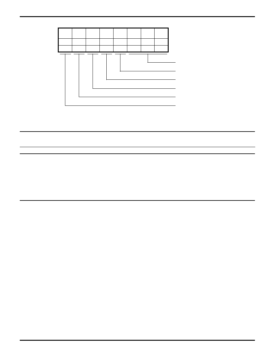
38
P R E L I M I N A R Y
Z80185/Z80195
S
MART
P
ERIPHERAL
C
ONTROLLERS
DS971850301
Zilog
MPBT
MP
/CTS/
PS
SS2
SS1
SS0
Invalid
R/W
0
R/W
R/W
0
R/W
0
R/W
1
R/W
1
R/W
1
R/W
R/W
CNTLB0
Clock Source and Speed Select
Addr 02H
Bit
Upon Reset
DR
PE0
Divide Ratio
Parity Even or Odd
Clear To Send/Prescale
Multiprocessor
Multiprocessor Bit Transmit
/CTS - Depending on the condition of /CTS pin.
PS - Cleared to 0.
General
PS = 0
PS = 1
Divide Ratio
(Divide Ratio = 10)
(Divide Ratio = 30)
SS, 2, 1, 0
DR = 0 (x16)
DR = 1 (x64)
DR = 0 (x16)
DR = 1 (x64)
000
ÿ
˜
160
ÿ
˜
640
ÿ
˜
480
ÿ
˜
1920
001
ÿ
˜
320
ÿ
˜
1280
ÿ
˜
960
ÿ
˜
3840
010
ÿ
˜
640
ÿ
˜
2560
ÿ
˜
1920
ÿ
˜
7680
011
ÿ
˜
1280
ÿ
˜
5120
ÿ
˜
3840
ÿ
˜
15360
100
ÿ
˜
2560
ÿ
˜
10240
ÿ
˜
7680
ÿ
˜
30720
101
ÿ
˜
5120
ÿ
˜
20480
ÿ
˜
15360
ÿ
˜
61440
110
ÿ
˜
10240
ÿ
˜
40960
ÿ
˜
30720
ÿ
˜
122880
111
External Clock (Frequency < ÿ)
Figure 24. ASCI Control Register B
(Ch. 0)

39
P R E L I M I N A R Y
Z80185/Z80195
S
MART
P
ERIPHERAL
C
ONTROLLES
DS971850301
Zilog
ASCI CHANNELS CONTROL REGISTERS
(Continued)
MPBT
MP
/CTS/
PS
SS2
SS1
SS0
Invalid
R/W
0
R/W
0
R/W
0
R/W
0
R/W
1
R/W
1
R/W
1
R/W
R/W
CNTLB1
Clock Source and Speed Select
Addr 03H
Bit
Upon Reset
DR
PE0
Divide Ratio
Parity Even or Odd
Read - Status of /CTS pin
Write - Select PS
Multiprocessor
Multiprocessor Bit Transmit
General
PS = 0
PS = 1
Divide Ratio
(Divide Ratio = 10)
(Divide Ratio = 30)
SS, 2, 1, 0
DR = 0 (x16)
DR = 1 (x64)
DR = 0 (x16)
DR = 1 (x64)
000
ÿ
˜
160
ÿ
˜
640
ÿ
˜
480
ÿ
˜
1920
001
ÿ
˜
320
ÿ
˜
1280
ÿ
˜
960
ÿ
˜
3840
010
ÿ
˜
640
ÿ
˜
2560
ÿ
˜
1920
ÿ
˜
7680
011
ÿ
˜
1280
ÿ
˜
5120
ÿ
˜
3840
ÿ
˜
15360
100
ÿ
˜
2560
ÿ
˜
10240
ÿ
˜
7680
ÿ
˜
30720
101
ÿ
˜
5120
ÿ
˜
20480
ÿ
˜
15360
ÿ
˜
61440
110
ÿ
˜
10240
ÿ
˜
40960
ÿ
˜
30720
ÿ
˜
122880
111
External Clock (Frequency < ÿ)
Figure 25. ASCI Control Register B
(Ch. 1)
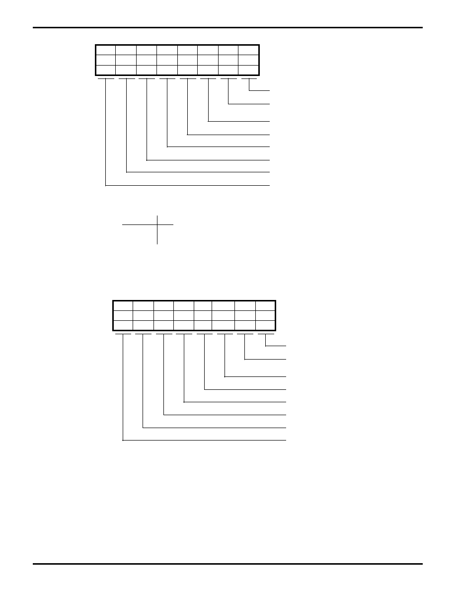
40
P R E L I M I N A R Y
Z80185/Z80195
S
MART
P
ERIPHERAL
C
ONTROLLERS
DS971850301
Zilog
Upon Reset
RDRF OVRN
/DCD0 TDRE
TIE
0
R
0
R
0
R
0
R
0
R/W
R
R
0
R/W
R/W
STAT0
Transmit Interrupt Enable
Addr 04H
Bit
RIE
FE
Transmit Data Register
Empty
Data Carrier Detect
Receive Interrupt Enable
Framing Error
Parity Error
PE
Over Run Error
Receive Data Register Full
/DCD0 - Depending on the condition of /DCD0 Pin.
/CTS0 Pin TDRE
L 1
H 0
Figure 26. ASCI Status Register
(Ch. 0)
RDRF OVRN
CTS1E TDRE
TIE
0
R
0
R
0
R
0
R
0
R/W
R/W
1
R
0
R/W
R/W
STAT1
Transmit Interrupt Enable
Addr 05H
Bit
Upon Reset
RIE
FE
Transmit Data Register
Empty
Reserved
Receive Interrupt Enable
Framing Error
Parity Error
PE
0
Over Run Error
Receive Data Register Full
Figure 27. ASCI Status Register
(Ch. 1)

41
P R E L I M I N A R Y
Z80185/Z80195
S
MART
P
ERIPHERAL
C
ONTROLLES
DS971850301
Zilog
RDRF Interrupt Inhibit
Send Break
0 = Normal Xmit
1 = Drive TXA Low
BRG0 Mode
0 = As S180
1 = Enable 16-bit BRG counter
X1 bit clk ASCI0
0 = CKA0 /16 or /64
1 = CKA0 is bit clock
CTS0 Disable
0 = CTS0 Auto-Enable Tx
1 = CTS0 Advisory to SW
DCD0 Disable
0 = DCD0 Auto-Enables Rx
1 = DCD0 Advisory to SW
Break Detect (RO)
Break Feature Enable
0
0
0
0
0
0
0
0
7
6
5
4
3
2
1
0
New Z8S180 Register
ASCI CHANNELS CONTROL REGISTERS
(Continued)
7
6
5
4
3
2
1
0
Transmit Data
TDR0
Write Only
Addr 06H
7
6
5
4
3
2
1
0
Transmit Data
TDR1
Write Only
Addr 07H
Figure 29. ASCI Transmit Data Register
(Ch. 1)
x
x
x
x
x
x
x
x
Received Data
TSR0
Read Only
Addr 08H
Figure 30. ASCI Receive Data Register
(Ch. 0)
x
x
x
x
x
x
x
x
Received Data
TSR1
Read Only
Addr 09H
Figure 31. ASCI Receive Data Register
(Ch. 1)
Figure 32. ASCI0 Extension Control Register
(I/O Address 12)
Figure 33. ASCI1 Extension Control Register
(I/O Address 13)
Figure 28. ASCI Transmit Data Register
(Ch. 0)
Break Feature Enable
Break Detect (RO)
Send Break
0 = Normal Xmit
1 = Drive TXA Low
BRG1 Mode
0 = As S180
1 = Enable 16-bit BRG Counter
X1 Bit CLK ASCI1
0 = CKA1 /16 or /64
1 = CKA1 is bit Clock
RDRF Interrupt Inhibit
0
0
0
0
0
0
0
0
7
6
5
4
3
2
1
0
New Z8S180 Register
Reserved (Program as 0)

42
P R E L I M I N A R Y
Z80185/Z80195
S
MART
P
ERIPHERAL
C
ONTROLLERS
DS971850301
Zilog
ACSI TIME CONSTANT REGISTERS
New Z8S180 Registers
7
6
5
4
3
2
1
0
7
6
5
4
3
2
1
0
Register:
ASCI0 Time Constant Low
Address:
1Ah
Register:
ASCI1 Time Constant Low
Address:
1Ch
7
6
5
4
3
2
1
0
7
6
5
4
3
2
1
0
Register:
ASCI0 Time Constant High
Address:
1Bh
Register:
ASCI1 Time Constant High
Address:
1Dh
CSI/O REGISTERS
EF
EIE
SS2
SS1
SS0
0
R
0
R/W
0
R/W
0
R/W
1
1
R/W
1
R/W
1
R/W
R/W
Speed Select
Addr 0AH
Bit
Upon Reset
-
TE
Transmit Enable
Receive Enable
End Interrupt Enable
End Flag
RE
CNTR
SS2, 1, 0
Baud Rate
000
ÿ
˜
20
001
ÿ
˜
40
010
ÿ
˜
80
011
ÿ
˜
100
SS2, 1, 0
Baud Rate
100
ÿ
˜
320
101
ÿ
˜
640
110
ÿ
˜
1280
111
External Clock
(Frequency < ÿ
˜
20)
Figure 34. CSI/O Control Register
Figure 35. CSI/O Transmit/Receive Data Register
7
6
5
4
3
2
1
0
Read - Received Data
Write - Transmit Data
TRDR
Read/Write
Addr 0BH

43
P R E L I M I N A R Y
Z80185/Z80195
S
MART
P
ERIPHERAL
C
ONTROLLES
DS971850301
Zilog
TIMER DATA REGISTERS
7
6
5
4
3
2
1
0
TMDR0L
Read/Write
Addr 0CH
Figure 36. Timer 0 Data Register L
7
6
5
4
3
2
1
0
TMDR1L
Read/Write
Addr 14H
Figure 37. Timer 1 Data Register L
15 14 13 12 11 10 9
8
TMDR0H
Read/Write
Addr 0DH
When Read, read Data Register L
before reading Data Register H.
Figure 38. Timer 0 Data Register H
15 14 13 12 11 10 9
8
TMDR1H
Read/Write
Addr 15H
When Read, read Data Register L
before reading Data Register H.
Figure 39. Timer 1 Data Register H
TIMER RELOAD REGISTERS
7
6
5
4
3
2
1
0
RLDR0L
Read/Write
Addr 0EH
Figure 40. Timer 0 Reload Register L
7
6
5
4
3
2
1
0
RLDR1L
Read/Write
Addr 16H
15 14 13 12 11 10 9
8
RLDR0H
Read/Write
Addr 0FH
Figure 42. Timer 0 Reload Register H
15 14 13 12 11 10 9
8
RLDR1H
Read/Write
Addr 17H
Figure 41. Timer 1 Reload Register L
Figure 43. Timer 1 Reload Register H

44
P R E L I M I N A R Y
Z80185/Z80195
S
MART
P
ERIPHERAL
C
ONTROLLERS
DS971850301
Zilog
TIMER CONTROL REGISTER
TIF1
TIF0
TOC0 TDE1 TDE0
0
R
0
R
0
R/W
0
R/W
0
R/W
R/W
0
R/W
0
R/W
R/W
TCR
Timer Down Count Enable 1,0
Addr 10H
Bit
Upon Reset
TOC1
TIE0
Timer Output Control 1,0
Timer Interrupt Enable 1,0
Timer Interrupt Flag 1,0
TIE1
0
TOC1,0 A15/TOUT
00
Inhibited
01
Toggle
10
0
11
1
Figure 44. Timer Control Register
FREE RUNNING COUNTER
Figure 45. Free Running Counter
7
6
5
4
3
2
1
0
FRC
Read Only
Addr 18H
CPU CONTROL REGISTER
0
0
0
0
0
0
0
0
CPU Control Register (CCR)
D7 D6 D5 D4 D3 D2 D1 D0
Addr 1FH
Figure 46. CPU Control Register
Note:
See Figure 87 for full description.
45
P R E L I M I N A R Y
Z80185/Z80195
S
MART
P
ERIPHERAL
C
ONTROLLES
DS971850301
Zilog
DMA REGISTERS
SAR0L
Read/Write
Addr 20H
SA7
SA0
SAR0H
Read/Write
Addr 21H
SA15
SA8
SAR0B
Read/Write
Addr 22H
SA16
SA19
-
-
-
-
Bits 0-3 are used for SAR0B
SM1-0
11
11
11
11
11
SAR18-16
000
001
010
011
111
Source
ext (TOUT/DREQ)
ASCI0 Rx
ASCI1 Rx
ESCC Rx
PIA27-20 IN
Figure 47. DMA 0 Source Address Registers
Figure 48. DMA 0 Destination Address Registers
DAR0L
Read/Write
Addr 23H
DA7
DA0
DAR0H
Read/Write
Addr 24H
DA15
DA8
DAR0B
Read/Write
Addr 25H
DA16
DA19
-
-
-
-
Bits 0-3 are used for DAR0B
DM1-0
11
11
11
11
11
DAR18-16
000
001
010
011
111
Destination
ext (TOUT/DREQ)
ASCI0 Tx
ASCI1 Tx
ESCC Tx
PIA27-20 OUT
46
P R E L I M I N A R Y
Z80185/Z80195
S
MART
P
ERIPHERAL
C
ONTROLLERS
DS971850301
Zilog
Figure 49. DMA 0 Byte Counter Registers
BCR0L
Read/Write
Addr 26H
BC7
BC0
BCR0H
Read/Write
Addr 27H
BC15
BC8
MAR1L
Read/Write
Addr 28H
MA7
MA0
MAR1H
Read/Write
Addr 29H
MA15
MA8
MAR1B
Read/Write
Addr 2AH
MA16
MA19
-
-
-
-
Figure 50. DMA 1 Memory Address Registers
D7
D6
D5
D4
D3
D2
D1
D0
Alternating Channels
0 = DMA Channels
are independent
1 = Toggle between DMA
channels for same device
Currently selected DMA
Channel when Bit 7 = 1
Reserved, program as 0.
0 = TOUT//DREQ is DREQ In
1 = TOUT//DREQ is TOUT Out
000 = DMA1 ext TOUT/DREQ
001 = DMA1 ASCI0
010 = DMA1 ASCI1
011 = DMA1 ESCC
111 = DMA1 PIA27-20 (P1284)
IAR1B
Addr 2D
New Z8S180 Register
Figure 51. DMA I/O Address Register Ch. 1

47
P R E L I M I N A R Y
Z80185/Z80195
S
MART
P
ERIPHERAL
C
ONTROLLES
DS971850301
Zilog
DMA REGISTER DESCRIPTION
Bit 7.
This bit should be set to 1 only when both DMA
channels are set to take their requests from the same
device. If this bit is 1 (it resets to 0), the channel end output
of DMA channel 0 sets a flip-flop, so that thereafter the
device's request is visible to channel 1, but is not visible to
channel 0. The channel end output of channel 1 clears the
FF, so that thereafter, the device's request is visible to
channel 0, but not visible to channel 1.
Bit 6.
When both DMA channels are programmed to take
their requests from the same device, this bit (FF mentioned
in the previous paragraph) controls which channel the
device's request is presented to: 0 = DMA 0, 1 = channel
1. When bit 7 is 1, this bit is automatically toggled by the
channel end output of the channels, as described above.
Bits 5-4.
Reserved and should be programmed as 0.
Bits 3.
This bit controls the direction and use of the TOUT/
DREQ pin. When it's 0, TOUT/DREQ is the DREQ input;
when it's 1, TOUT/DREQ is an output that can carry the
TOUT signal from PRT1, if PRT1 is so programmed.
Bits 2-0.
With "DIM1", bit 1 of DCNTL, these bits control
which request is presented to DMA channel 1, as follows:
DIM1 IAR18-16
Request Routed to DMA Channel 1
0
000
ext TOUT/DREQ
0
001
ASCI0 Tx
0
010
ASCI1 Tx
0
011
EMSCC out
0
10X
Reserved, do not program.
0
1X0
Reserved, do not program.
0
111
PIA27-20 out
1
000
ext TOUT/DREQ
1
001
ASCI0 Rx
1
010
ASCI1 Rx or TOUT//DREQ pin
1
011
EMSCC in
1
10X
Reserved, do not program.
1
1X0
Reserved, do not program.
1
111
PIA27-20 in
IAR1L
Read/Write
Addr 2BH
IA7
IA0
IAR1H
Read/Write
Addr 2CH
IA15
IA8
Figure 52. DMA I/O Address Registers
BCR1L
Read/Write
Addr 2EH
BC7
BC0
BCR1H
Read/Write
Addr 2FH
BC15
BC8
Figure 53. DMA 1 Byte Count Registers
DE1
DE0
DIE0
-
DIME
0
R/W
0
R/W
1
W
1
W
0
0
R/W
1
0
R
R/W
DMA Master Enable
Addr 30H
Bit
Upon Reset
DIE1
/DWE0
DMA Interrupt Enable 1, 0
DMA Enable Bit Write Enable 1, 0
DMA Enable Ch 1, 0
/DWE1
DSTAT
R/W
Figure 54. DMA Status Register

48
P R E L I M I N A R Y
Z80185/Z80195
S
MART
P
ERIPHERAL
C
ONTROLLERS
DS971850301
Zilog
DMA REGISTERS
(Continued)
-
-
SM0
MMOD
-
1
1
0
R/W
0
R/W
0
0
R/W
0
1
R/W
Memory MODE Select
Addr 31H
Bit
Upon Reset
SM1
DM0
Ch 0 Source Mode 1, 0
Ch 0 Destination Mode 1, 0
DM1
DMODE
R/W
R/W
DM1, 0
00
01
10
11
Destination
M
M
M
I/O
Address
DAR0+1
DAR0-1
DAR0 Fixed
DAR0 Fixed
SM1, 0
00
01
10
11
Source
M
M
M
I/O
Address
SAR0+1
SAR0-1
SAR0 Fixed
SAR0 Fixed
0
1
Mode
Cycle Steal Mode
Burst Mode
MMOD
Figure 55. DMA Mode Registers

49
P R E L I M I N A R Y
Z80185/Z80195
S
MART
P
ERIPHERAL
C
ONTROLLES
DS971850301
Zilog
DMA REGISTERS
(Continued)
MWI1
MWI0
DMS0
DIM1
DIM0
1
1
1
R/W
1
R/W
0
0
R/W
0
0
R/W
DMA Ch 1 I/O Memory
Mode Select
Addr 32H
Bit
Upon Reset
DMS1
IWI0
/DREQi Select, i = 1, 0
I/0 Wait Insertion
IWI1
DCNTL
R/W
R/W
R/W
R/W
R/W
Memory Wait Insertion
DM1, 0
00
01
10
11
Transfer Mode
M - I/O
M - I/O
I/O - M
I/O - M
Address Increment/Decrement
DMSi
1
0
Sense
Edge Sense
Level Sense
MWI1, 0
00
01
10
11
No. of Wait States
0
1
2
3
IWI1, 0
00
01
10
11
No. of Wait States
1
2
3
4
MAR1+1
MAR1-1
IAR1 Fixed
IAR1 Fixed
IAR1 Fixed
IAR1 Fixed
MAR1+1
MAR1-1
*
Note:
* If using the Wait-State Generators provided in
register D8, the MWI1-0 bits should be set to 00.
Figure 56. DMA/WAIT Control Register

50
P R E L I M I N A R Y
Z80185/Z80195
S
MART
P
ERIPHERAL
C
ONTROLLERS
DS971850301
Zilog
SYSTEM CONTROL REGISTERS
IL7
IL6
-
-
-
0
0
0
R/W
0
0
0
0
0
R/W
Interrupt Vector Low
Addr 33H
Bit
Upon Reset
-
-
IL5
IL
R/W
R/W
Figure 57. Interrupt Vector Low Register
TRAP UFO
ITE2
ITE1
ITE0
0
0
1
1
1
0
R/W
0
1
R/W
/INT Enable 2, 1, 0
Addr 34H
Bit
Upon Reset
-
-
-
ITC
R/W
R
R/W
R/W
Undefined Fetch Object
TRAP
Figure 58. INT/TRAP Control Register
REFE REFW
-
CYC1 CYC0
1
1
1
1
1
1
0
0
R/W
Cycle Select
Addr 36H
Bit
Upon Reset
-
-
Refresh Wait State
Refresh Enable
-
RCR
R/W
R/W
R/W
R/W
CYC1, 0
00
01
10
11
Interval of Refresh Cycle
10 states
20 states
40 states
80 states
Figure 59. Refresh Control Register

51
P R E L I M I N A R Y
Z80185/Z80195
S
MART
P
ERIPHERAL
C
ONTROLLES
DS971850301
Zilog
MMU REGISTERS
CB7
CB6
CB2
CB1
CB0
0
0
0
R/W
0
R/W
0
0
R/W
0
0
R/W
MMU Common Base
Register
Addr 38H
Bit
Upon Reset
CB3
CB4
CB5
CBR
R/W
R/W
R/W
R/W
R/W
Figure 60. MMU Common Base Register
BB7
BB6
BB2
BB1
BB0
0
0
0
R/W
0
R/W
0
0
R/W
0
0
R/W
MMU Bank Base Register
Addr 39H
Bit
Upon Reset
BB3
BB4
BB5
BBR
R/W
R/W
R/W
R/W
R/W
Figure 61. MMU Bank Base Register
CA3
CA2
BA2
BA1
BA0
1
1
1
R/W
1
R/W
0
0
R/W
0
0
R/W
MMU Bank Area Register
Addr 3AH
Bit
Upon Reset
BA3
CA0
CA1
CBAR
R/W
R/W
R/W
R/W
R/W
MMU Common Area Register
Figure 62. MMU Common/Bank Area Register

52
P R E L I M I N A R Y
Z80185/Z80195
S
MART
P
ERIPHERAL
C
ONTROLLERS
DS971850301
Zilog
SYSTEM CONTROL REGISTERS
Figure 63. Operation Mode Control Register
M1E /M1TE
-
-
-
1
1
1
1
1
1
1
1
R/W
I/O Compatibility
Addr 3EH
Bit
Upon Reset
-
-
/M1 Temporary Enable
/M1 Enable
/IOC
OMCR
W
R/W
R/W
Notes:
1. This register should be programmed to 0x0xxxxxb
(x = don't care) as a part of Initialization.
2. If the M1E bit is set to 1, the processor does not
fetch a RETI instruction.
IOA7
IOA6
-
-
-
0
0
0
1
1
1
1
1
R/W
I/O Stop
Addr 3FH
Bit
Upon Reset
-
-
I/O Address
Combination of 11
is reserved
IOSTP
ICR
R/W
R/W
R/W
Figure 64. I/O Control Register
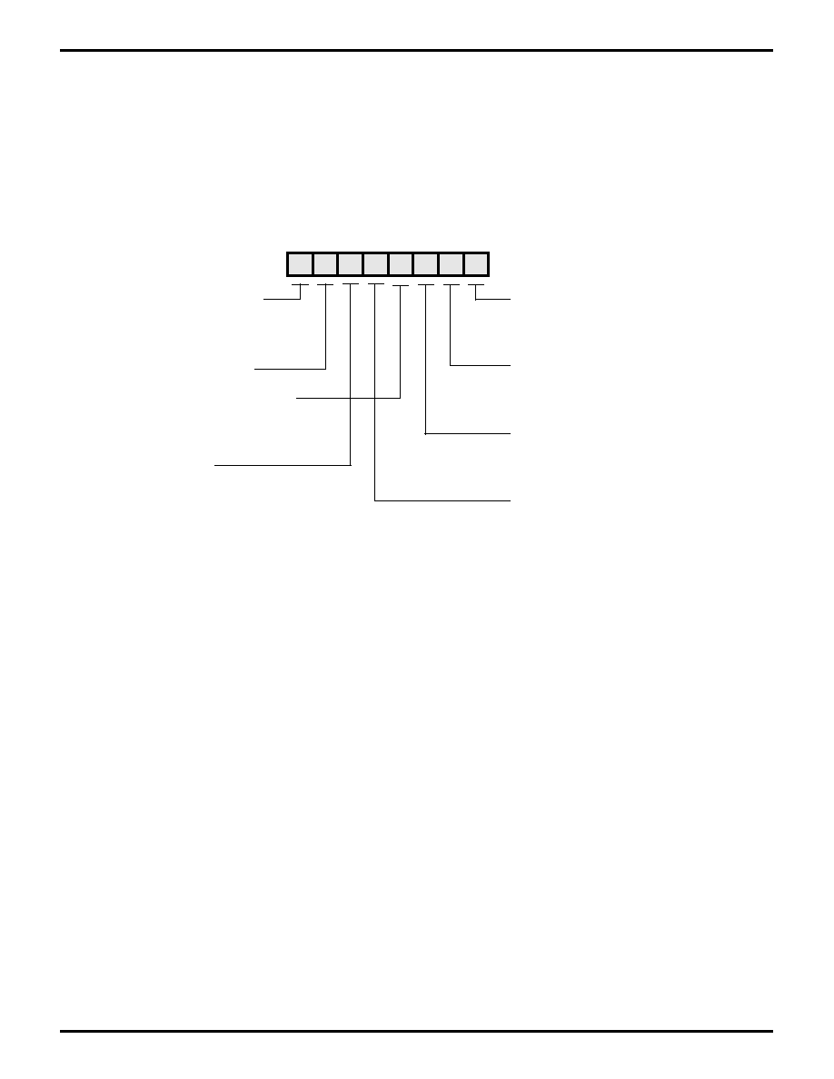
53
P R E L I M I N A R Y
Z80185/Z80195
S
MART
P
ERIPHERAL
C
ONTROLLES
DS971850301
Zilog
CPU CONTROL REGISTER
The CPU Control Register allows the programmer to select
options that directly affect the CPU performance as well as
controlling the STANDBY operating mode of the chip. The
CPU Control Register (CCR) allows the programmer to
change the divide-by-two internal clock to divide-by-one.
In addition, applications where EMI noise is a problem, the
Z8S180 can reduce the output drivers on selected groups
of pins to 33 percent of normal pad driver capability which
minimizes the EMI noise generated by the part (Figure 65).
0
0
0
0
0
0
0
0
D7 D6 D5 D4 D3 D2 D1 D0
LNCPUCTL
0 = Standard Drive
1 = 33% Drive On CPU
Control Signals
CPU Control Register (CCR) Addr 1FH
LNAD/DATA
0 = Standard Drive
1 = 33% Drive On
A19-A0, D7-D0
LNIO
0 = Standard Drive
1 = 33% Drive on Certain
External I/O
Standby/Idle Enable
00 = No Standby
01 = Idle After Sleep
10 = Standby After Sleep
11 = Standby After Sleep
64 Cycle Exit
(Quick Recovery)
LNPHI
0 = Standard Drive
1 = 33% Drive On
EXT.PHI Clock
BREXT
0 = Ignore BUSREQ
In Standby/Idle
1 = Standby/Idle Exit
on BUSREQ
Clock Divide
0 = XTAL/2
1 = XTAL/1
New Z8S180 Register
Figure 65. CPU Control Register

54
P R E L I M I N A R Y
Z80185/Z80195
S
MART
P
ERIPHERAL
C
ONTROLLERS
DS971850301
Zilog
Bit 7.
Clock Divide Select. Bit 7 of the CCR allows the
programmer to set the internal clock to divide the external
clock by two if the bit is 0 and divide-by-one if the bit is 1.
Upon reset, this bit is set to 0 and the part is in
divide-by-two mode. Since the on-board oscillator is not
guaranteed to operate above 20 MHz, an external source
must be used to achieve the maximum 33 MHz operation
of the device, such as an external clock at 66 MHz with 50
percent duty cycle.
If an external oscillator is used in divide-by-one mode, the
minimum pulse width requirement must be satisfied.
Bits 6 and 3.
STANDBY/IDLE Enable. These two bits are
used for enabling/disabling the IDLE and STANDBY mode.
Setting D6, D3 to 0 and 1, respectively, enables the IDLE
mode. In the IDLE mode, the clock oscillator is kept
oscillating but the clock to the rest of the internal circuit,
including the CLKOUT, is stopped. The Z8S180 enters
IDLE mode after fetching the second opcode of a SLEEP
instruction, if the I/O STOP bit is set.
Setting D6, D3 to 1 and 0, respectively, enables the
STANDBY mode. In the STANDBY mode, the clock oscil-
lator is stopped completely. The Z8S180 enters STANDBY
after fetching the second opcode of a SLEEP instruction,
if the I/O STOP bit is set.
Setting D6, D3 to 1 and 1, respectively, enables the
STANDBY-QUICK RECOVERY mode. In this mode, its
operations are identical to STANDBY except that the clock
recovery is reduced to 64 clock cycles after the exit
conditions are gathered. Similarly, in STANDBY mode, the
Z8S180 enters STANDBY after fetching the second opcode
of a SLEEP instruction, if the I/O STOP bit is set.
Bit 5.
BREXT. This bit controls the ability of the Z8S180 to
honor a bus request during STANDBY mode. If this bit is
set to 1 and the part is in STANDBY mode, a BUSREQ is
honored after the clock stabilization timer is timed out.
Bit 4.
LNPHI. This bit controls the drive capability on the
PHI Clock output. If this bit is set to 1, the PHI Clock output
is reduced to 33 percent of its drive capability.
Bit 2.
LNIO. This bit controls the drive capability of certain
external I/O pins on the Z8S180. When this bit is set to 1,
the output drive capability of the following pins is reduced
to 33 percent of the original drive capability:
/RTS0/TXS
TXA0
CKA1
TXA1
CKA0
TOUT
Bit 1.
LNCPUCTL. This bit controls the drive capability of
the CPU Control pins. When this bit is set to 1, the output
drive capability of the following pins is reduced to 33
percent of the original drive capability:
/BUSACK
/IORQ
/RD
/RFSH
/WR
/HALT
/M1
ST
/MREQ
Bit 0.
LNAD/DATA. This bit controls the drive capability of
the Address/Data bus output drivers. If this bit is set to 1,
the output drive capability of the Address and Data bus
output is reduced to 33 percent of its original drive capa-
bility.

55
P R E L I M I N A R Y
Z80185/Z80195
S
MART
P
ERIPHERAL
C
ONTROLLES
DS971850301
Zilog
ON-CHIP ENHANCED SERIAL COMMUNICATIONS CONTROLLER (EMSCC)
The Z80185 contains a single-channel EMSCC which
features a 4-byte transmit FIFO and an 8-byte receive
FIFO, this enhancement reduces the overhead required to
provide data to, and get data from, the transmitter and
receiver. The EMSCC also improves packet handling in
SDLC mode to:
s
automatically transmit a flag before the data;
s
reset the Tx Underrun/EOM latch;
s
force the TxD pin High at the appropriate time when
using NRZI encoding;
s
deassert the /RTS pin after the closing flag;
and
s
better handle ABORTed frames when using the 10x19
status FIFO.
The combination of these features, along with the data
FIFOs, significantly simplifies SDLC driver software.
The CPU hardware interface has been simplified by reliev-
ing the databus setup time requirement and supporting
the software generation of the interrupt acknowledge sig-
nal (/INTACK). These changes allow an interface with less
external logic to many microprocessor families while main-
taining compatibility with existing designs. I/O handling of
the EMSCC is improved over the SCC, with faster response
of the /DTR//REQ pin. The many enhancements added to
the EMSCC permits a system design that increases overall
system performance with better data handling and less
interface logic.
Significant features of the EMSCC include:
s
Hardware and software compatible with Zilog's SCC/
ESCC
s
4-Byte Transmit FIFO
s
8-Byte Receive FIFO
s
Programmable FIFO Interrupt Levels Provide Flexible
Interrupt Response
s
Improved SDLC Frame Status FIFO
s
New Programmable Features Added with Write
Register 7'
s
Write registers: WR3, WR4, WR5, and WR10 are now
readable
s
Read Register 0 Latched During Access
s
Many Improvements to Support SDLC/HDLC Transfers:
≠ Deactivation of /RTS Pin after Closing Flag
≠ Automatic Transmission of the Opening Flag
≠ Automatic Reset of Tx Underrun/EOM Latch
≠ Complete CRC Reception
≠ TxD pin Automatically Forced High with NRZI
Encoding when Using Mark Idle.
≠ Receive FIFO Automatically Unlocked for
Special Receive Interrupts when Using the
SDLC Status FIFO.
≠ Back-to-Back Frame Transmission Simplified
s
Software Interrupt Acknowledge mode
s
DPLL Counter Output Available as Jitter-Free Clock
Source
s
A Full-Duplex Channel with a Baud Rate Generator
and Digital Phase-Locked Loop
s
Multi-Protocol Operation Under Program Control
s
Asynchronous or Synchronous mode
In addition, the following features have been added to the
EMSCC
channel in the Z80185:
s
Programmable LocalTalk feature
s
Non-Multiplexed /DTR Pin
s
Internal Connection of DMA Request and /WAIT Signals
s
EMSCC Programmable Clock
≠ Programmed to be Equal to System Clock
Divided by One or Two
≠ Programmed by System Configuration Register
Note:
The EMSCC programmable clock must be pro-
grammed to divide-by-two mode when operating above
the following condition: PHI > 20 MHz at 5.0V
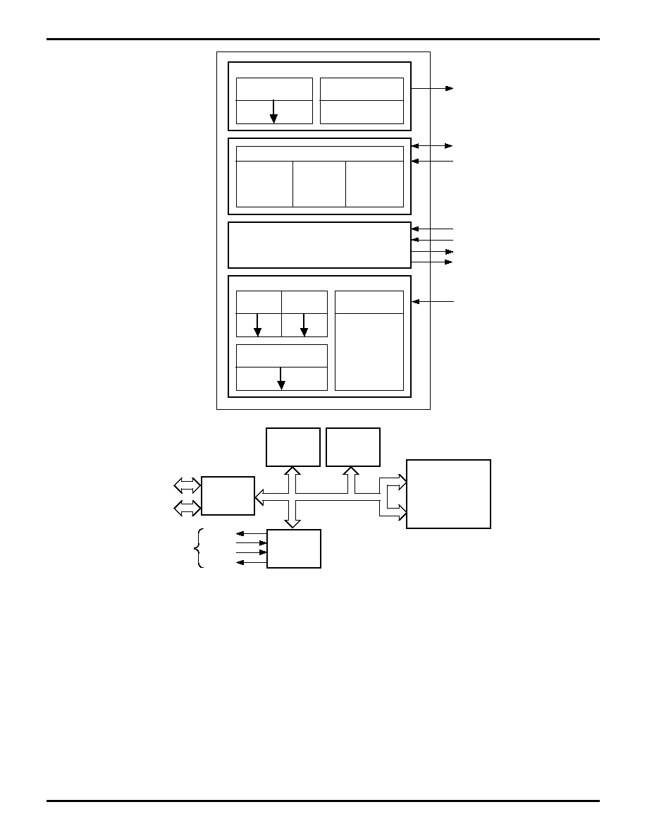
56
P R E L I M I N A R Y
Z80185/Z80195
S
MART
P
ERIPHERAL
C
ONTROLLERS
DS971850301
Zilog
Transmit Logic
Receive and Transmit Clock Multipexer
Transmit FIFO
4 Bytes
Transmit MUX
Data Encoding & CRC
Generation
Digital
Phase-Locked
Loop
Baud Rate
Generator
Crystal
Oscillator
Amplifier
Modem/Control Logic
Receive MUX
CRC Checker,
Data Decode &
Sync Character
Detection
Rec. Status
FIFO 8-Byte
Rec. Data
FIFO 8-Byte
SDLC Frame Status FIFO
10 x 19
Receive Logic
TxD
/TRxC
/RTxC
/CTS
/DCD
/RTS
/DTR
RxD
Interrupt
Control
Logic
Databus
Control
CPU & DMA
Bus Interface
/INT
/INTACK
IEI
IEO
Interrupt
Control
Channel A
Tx-Rx
Internal
Control
Logic
Channel A
Register
Figure 66. EMSCC Block Diagram

57
P R E L I M I N A R Y
Z80185/Z80195
S
MART
P
ERIPHERAL
C
ONTROLLES
DS971850301
Zilog
EMSCC
The Z80185 features a one-channel EMSCC that uses two
I/O addresses:
EMSCC Channel A Control
I/O Address %E8
Data
I/O Address %E9
Divide-by-two should be programmed when operating the
Z80185 beyond 20 MHz, 5V.
Note:
Upon power-up, or reset, the system clock is equal
to the EMSCC clock.
Initialization.
The system program first issues a series of
commands to initialize the basic mode of operation. This is
followed by other commands to qualify conditions within
the selected mode. For example, in the Asynchronous
mode, character length, clock rate, number of stop bits,
and even or odd parity should be set first. Then the
interrupt mode is set, and finally, the receiver and transmit-
ter are enabled.
Write Registers.
The EMSCC contains 16 write registers
(17 counting the transmit buffer) in each channel. These
write registers are programmed separately to configure
the functional "personality" of the channels. A new register,
WR7', was added to the EMSCC and may be written to if
WR15, D0 is set. Figure 50 shows the format of each write
register.
Read Registers.
The EMSCC contains ten read registers
(11 counting the receive buffer) in each channel. Four of
these may be read to obtain status information (RR0, RR1,
RR10, and RR15). Two registers (RR12 and RR13) are
read to learn the baud rate generator time constant. RR2
contains either the unmodified interrupt vector (channel A)
or the vector modified by status information (channel B).
RR3 contains the Interrupt Pending (IP) bits (channel A
only). RR6 and RR7 contain the information in the SDLC
Frame Status FIFO, but is only read when WR15 D2 is set.
If WR7' D6 is set, Write Registers WR3, WR4, WR5, WR7,
and WR10 can be read as RR9, RR4, RR5, and RR14,
respectively. Figure 51 shows the format of each read
register.
With the Z80185, the EMSCC channel's DTR, Tx and Rx
DMA Request and WAIT outputs are not subject to multi-
plexing and are routed separately to the CPU and pins.
In other words,
1. the DTR pin is not multiplexed and always follows WR5
bit 7;
2. if WR1 bits 7-6 are 10, and the processor reads the RDR
when the RxFIFO is empty, or writes the TDR when the
TxFIFO is full, the processor is "waited" until a character
arrives or has been sent out;
3. WR1 bit 5 has no effect;
4. WR14 bit 2 should be kept 0;
5. WR1 bits 7-6 should not be programmed as 11.
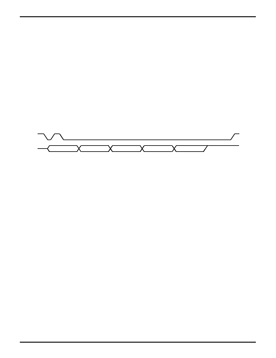
58
P R E L I M I N A R Y
Z80185/Z80195
S
MART
P
ERIPHERAL
C
ONTROLLERS
DS971850301
Zilog
A LocalTalk feature has been added in one EMSCC of the
Z80185, operating as follows:
If a certain set of register bits are set, RTS acts as a
LocalTalk Driver Enable output that operates as shown in
Figure 50. All of the following bits and fields must be
programmed exactly as shown to enable this mode:
WR4.3-2 = 00: sync modes
WR4.5-4 = 10: SDLC
WR5.1
=
0: no RTS
WR7'.2
=
1: auto RTS deactivation
WR10.3
=
1: mark idle
WR5.4
=
1: Send Break
When the first five conditions above are set (as for LocalTalk
operation), the WR5.4 bit is used as a Select LocalTalk
Driver Enable control bit, rather than the Send Break
command bit used in async mode.
Setting these register bits in this manner configures the
EMSCC Transmitter to send three Flags before a frame,
negating RTS during the first to create a coding violation,
when software writes the first character of a frame to the
TDR and TxFIFO. This mode also makes the Transmitter
ensure at least 16 bits of idle time between a closing Flag
and the end of frame interrupt. The RTS output is driven
active for one bit time at the start of the first of the three
Flags, then inactive for four bit times, then active again for
the duration of the opening Flags, the frame, and closing
Flag, plus 16 bit times thereafter.
There is one other difference in EMSCC operation when
this new mode is enabled. The setting of the TxIP bit, that
normally occurs after the last bit of the CRC is sent, is
delayed until the 16-bit Idle is sent and RTS is negated.
Flag
Frame
16-Bit Idle
RTS
TxD
Flag
Flag
Flag
Figure 67. EMSCC Transmitter Flag Commands
59
P R E L I M I N A R Y
Z80185/Z80195
S
MART
P
ERIPHERAL
C
ONTROLLES
DS971850301
Zilog
EMSCC REGISTERS
D7
D6
D5
D4
D3
D2
D1
D0
0 0 0 Register 0
0 0 1 Register 1
0 1 0 Register 2
0 1 1 Register 3
1 0 0 Register 4
1 0 1 Register 5
1 1 0 Register 6
1 1 1 Register 7
0 0 0 Register 8
0 0 1 Register 9
0 1 0 Register 10
0 1 1 Register 11
1 0 0 Register 12
1 0 1 Register 13
1 1 0 Register 14
1 1 1 Register 15
With Point High Command
*
*
Write Register 0 (non-multiplexed bus mode)
0 0 0 Null Code
0 0 1 Point High
0 1 0 Reset Ext/Status Interrupts
0 1 1 Send Abort (SDLC)
1 0 0 Enable Int on Next Rx Character
1 0 1 Reset Tx Int Pending
1 1 0 Error Reset
1 1 1 Reset Highest IUS
0 0 Null Code
0 1 Reset Rx CRC Checker
1 0 Reset Tx CRC Generator
1 1 Reset Tx Underrun/EOM Latch
D7
D6
D5
D4
D3
D2
D1
D0
V0
Write Register 2
V1
V2
V3
V4
V5
V6
V7
Interrupt
Vector
D7
D6
D5
D4
D3
D2
D1
D0
Write Register 1
Ext Int Enable
Tx Int Enable
Parity is Special Condition
0 0 Rx Int Disable
0 1 Rx Int On First Character or Special Condition
1 0 Int On All Rx Characters or Special Condition
1 1 Rx Int On Special Condition Only
Reserved,
Program as 00.
WAIT Request Enable
D7
D6
D5
D4
D3
D2
D1
D0
Write Register 4
Parity Enable
0 0 X1 Clock Mode
0 1 X16 Clock Mode
1 0 X32 Clock Mode
1 1 X64 Clock Mode
Parity EVEN//ODD
0 0 Sync Modes Enable
0 1 1 Stop Bit/Character
1 0 1 1/2 Stop Bits/Character
1 1 2 Stop Bits/Character
0 0 8-Bit Sync Character
0 1 16-Bit Sync Character
1 0 SDLC Mode (01111110 Flag)
1 1 External Sync Mode
D7
D6
D5
D4
D3
D2
D1
D0
Write Register 3
Rx Enable
0 0 Rx 5 Bits/Character
0 1 Rx 7 Bits/Character
1 0 Rx 6 Bits/Character
1 1 Rx 8 Bits/Character
Sync Character Load Inhibit
Address Search Mode (SDLC)
Rx CRC Enable
Enter Hunt Mode
Auto Enables
Figure 68. Write Register Bit Functions
60
P R E L I M I N A R Y
Z80185/Z80195
S
MART
P
ERIPHERAL
C
ONTROLLERS
DS971850301
Zilog
D7 D6 D5 D4 D3 D2 D1 D0
Write Register 5
Tx CRC Enable
0 0 Tx 5 Bits(Or Less)/Character
0 1 Tx 7 Bits/Character
1 0 Tx 6 Bits/Character
1 1 Tx 8 Bits/Character
RTS
/SDLC/CRC-16
Tx Enable
Send Break (Async Mode)
LocalTalk Driven Enable (HDLC Mode)
DTR
D7 D6 D5 D4 D3 D2 D1 D0
Write Register 6
Sync3
Sync3
Sync3
1
ADR3
x
Sync2
Sync2
Sync2
1
ADR2
x
Sync1
Sync1
Sync1
1
ADR1
x
Sync0
Sync0
Sync0
1
ADR0
x
Monosync, 8 Bits
Monosync, 6 Bits
Bisync, 16 Bits
Bisync, 12 Bits
SDLC
SDLC (Address Range)
Sync4
Sync4
Sync4
Sync0
ADR4
ADR4
Sync5
Sync5
Sync5
Sync1
ADR5
ADR5
Sync6
Sync0
Sync6
Sync2
ADR6
ADR6
Sync7
Sync1
Sync7
Sync3
ADR7
ADR7
D7 D6 D5 D4 D3 D2 D1 D0
Write Register 7
Sync3
Sync1
Sync11
Sync7
1
Sync2
Sync0
Sync10
Sync6
1
Sync1
x
Sync9
Sync5
1
Sync0
x
Sync8
Sync4
0
Monosync, 8 Bits
Monosync, 6 Bits
Bisync, 16 Bits
Bisync, 12 Bits
SDLC
Sync4
Sync2
Sync12
Sync8
1
Sync5
Sync3
Sync13
Sync9
1
Sync6
Sync4
Sync14
Sync10
1
Sync7
Sync5
Sync15
Sync11
0
Figure 69. Write Register Bit Functions
(Continued)
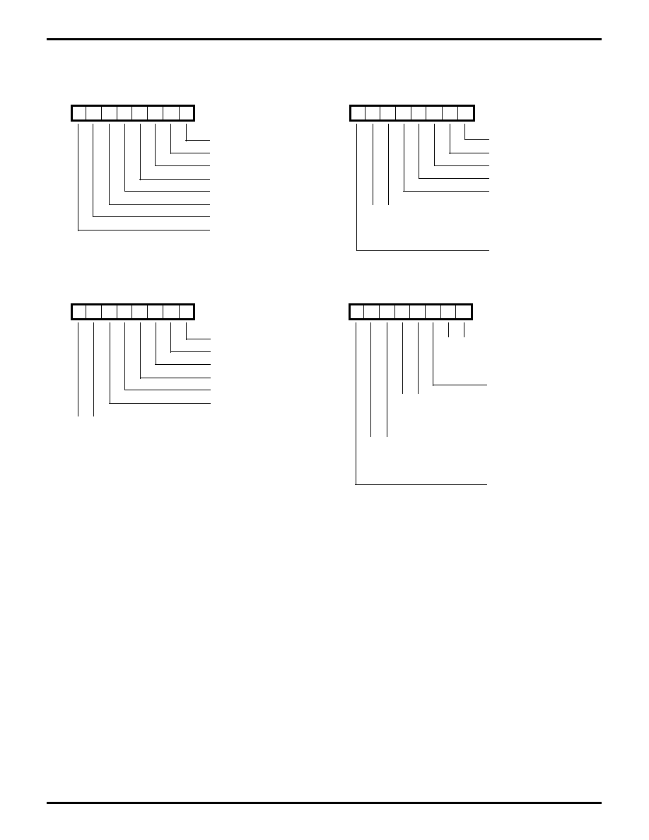
61
P R E L I M I N A R Y
Z80185/Z80195
S
MART
P
ERIPHERAL
C
ONTROLLES
DS971850301
Zilog
EMSCC REGISTERS
(Continued)
D7 D6 D5 D4 D3 D2 D1 D0
Write Register 10
6-Bit//8-Bit Sync
0 0 NRZ
0 1 NRZI
1 0 FM1 (Transition = 1)
1 1 FM0 (Transition = 0)
Loop Mode
Abort//Flag On Underrun
Mark//Flag Idle
Go Active On Poll
CRC Preset I//O
D7 D6 D5 D4 D3 D2 D1 D0
WR' Prime
Auto Tx Flag
Auto EOM Reset
Auto RTS Deactivation
Rx FIFO Int Level
Tx DMA Request Timing Mode
Tx FIFO Int Level
Extended Read Enable
32-Bit CRC Enable
D7 D6 D5 D4 D3 D2 D1 D0
Write Register 11
0 0 /TRxC Out = Xtal Output
0 1 /TRxC Out = Transmit Clock
1 0 /TRxC Out = BR Generator Output
1 1 /TRxC Out = DPLL Output
/TRxC O/I
0 0 Transmit Clock = /RTxC Pin
0 1 Transmit Clock = /TRxC Pin
1 0 Transmit Clock = BR Generator Output
1 1 Transmit Clock = DPLL Output
0 0 Receive Clock = /RTxC Pin
0 1 Receive Clock = /TRxC Pin
1 0 Receive Clock = BR Generator Output
1 1 Receive Clock = DPLL Output
Reserved
D7 D6 D5 D4 D3 D2 D1 D0
Write Register 9
VIS
0 0 No Reset
0 1 Not used
1 0 Channel Reset
1 1 Force Hardware Reset
NV
DLC
MIE
Status High//Status Low
Software INTACK Enable
Figure 70. Write Register Bit Functions
(Continued)
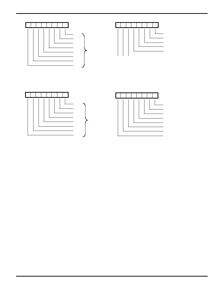
62
P R E L I M I N A R Y
Z80185/Z80195
S
MART
P
ERIPHERAL
C
ONTROLLERS
DS971850301
Zilog
D7 D6 D5 D4 D3 D2 D1 D0
TC0
Write Register 12
TC1
TC2
TC3
TC4
TC5
TC6
TC7
Lower Byte of
Time Constant
D7 D6 D5 D4 D3 D2 D1 D0
Write Register 14
0 0 0 Null Command
0 0 1 Enter Search Mode
0 1 0 Reset Missing Clock
0 1 1 Disable DPLL
1 0 0 Set Source = BR Generator
1 0 1 Set Source = /RTxC
1 1 0 Set FM Mode
1 1 1 Set NRZI Mode
BR Generator Enable
BR Generator Source
Reserved, Program as 0.
Auto Echo
Local Loopback
D7 D6 D5 D4 D3 D2 D1 D0
WR7' SDLC Feature Enable
Write Register 15
Zero Count IE
SDLC FIFO Enable
DCD IE
Sync/Hunt IE
CTS IE
Tx Underrun/EOM IE
Break/Abort IE
D7 D6 D5 D4 D3 D2 D1 D0
TC8
Write Register 13
TC9
TC10
TC11
TC12
TC13
TC14
TC15
Upper Byte of
Time Constant
Figure 71. Write Register Bit Functions
(Continued)

63
P R E L I M I N A R Y
Z80185/Z80195
S
MART
P
ERIPHERAL
C
ONTROLLES
DS971850301
Zilog
EMSCC REGISTERS
(Continued)
D7
D6
D5
D4
D3
D2
D1
D0
0
Read Register 3
0
0
Ext/Status IP
Tx IP
Rx IP
0
0
D7
D6
D5
D4
D3
D2
D1
D0
Rx Character Available
Read Register 0
Zero Count
Tx Buffer Empty
DCD
Sync/Hunt
CTS
Tx Underrun/EOM
Break/Abort
D7
D6
D5
D4
D3
D2
D1
D0
All Sent
Read Register 1
Residue Code 2
Residue Code 1
Residue Code 0
Parity Error
Rx Overrun Error
CRC/Framing Error
End of Frame (SDLC)
D7
D6
D5
D4
D3
D2
D1
D0
BC0
Read Register 6*
BC1
BC2
BC3
BC4
BC5
BC6
BC7
*Can only be accessed if the SDLC FIFO enhancement
is enabled (WR15 bit D2 set to 1)
SDLC FIFO Status and Byte Count (LSB)
D7
D6
D5
D4
D3
D2
D1
D0
V0
Read Register 2
V1
V2
V3
V4
V5
V6
V7
Interrupt
Vector
D7
D6
D5
D4
D3
D2
D1
D0
BC8
Read Register 7*
BC9
BC10
BC11
BC12
BC13
FDA: FIFO Data Available
1 = Status Reads from FIFO
0 = Status Reads from EMSCC
*Can only be accessed if the SDLC FIFO enhancement
is enabled (WR15 bit D2 set to 1)
SDLC FIFO Status and Byte Count (LSB)
FOS: FIFO Overflow Status
1 = FIFO Overflowed
0 = Normal
Figure 72. Read Register Bit Functions

64
P R E L I M I N A R Y
Z80185/Z80195
S
MART
P
ERIPHERAL
C
ONTROLLERS
DS971850301
Zilog
D7
D6
D5
D4
D3
D2
D1
D0
0
Read Register 10
On Loop
0
0
Loop Sending
0
Two Clocks Missing
One Clock Missing
D7
D6
D5
D4
D3
D2
D1
D0
TC8
Read Register 13
TC9
TC10
TC11
TC12
TC13
TC14
TC15
Upper Byte
of Time Constant
D7
D6
D5
D4
D3
D2
D1
D0
TC0
Read Register 12
TC1
TC2
TC3
TC4
TC5
TC6
TC7
Lower Byte
of Time Constant
D7
D6
D5
D4
D3
D2
D1
D0
0
Read Register 15
Zero Count IE
SDLC Status FIFO Enable
DCD IE
Sync/Hunt IE
CTS IE
Tx Underrun/EOM IE
Break/Abort IE
Figure 73. Read Register Bit Functions
(Continued)

65
P R E L I M I N A R Y
Z80185/Z80195
S
MART
P
ERIPHERAL
C
ONTROLLES
DS971850301
Zilog
P1284 REGISTER MAP
Register Name
I/O Addr/Access
PARM Register
%D9 R/W
PARC Register
(asymmetric)
%DA R/W
PARC2 Register
%DB WO
PART Register
%DC R/W
PARV Register
%DD R/W
Z80185 BIDIRECTIONAL CENTRONICS P1284 CONTROLLER
The Centronics P1284 Controller can operate in either the
Host or Peripheral role in Compatibility mode (host to
printer), Nibble or Byte mode (printer to host), and ECP
mode (bidirectional). It provides no hardware support for
the EPP mode, although it may be possible to implement
this mode by software.
Nine control signals have dedicated hardware pins, and
have
±
12 mA drive (P1284 Level 2) capability as does the
8-bit data port PIA27-20.
Note:
Signal names listed below
are those for the original Compatible mode. The names
shown in parentheses represent the same signal, but in a
more recent mode. The Z80185 does not include hardware
support for the P1284 EPP mode.
The following signals are outputs in a Peripheral mode,
inputs in a Host mode:
s
Busy (PtrBusy, PeriphAck)
s
nAck (PtrClk, PeriphClk)
s
PError (AckDataReq, nAckReverse)
s
nFault (nDataAvail, nPeriphRequest)
s
Select (Xflag)
The following signals are inputs in a Peripheral mode,
outputs in a Host mode:
s
nStrobe (HostClk)
s
nAutoFd (HostBusy, HostAck)
s
nSelectIn (P1284Active)
s
nInit (nReverseRequest)
Note that, because the Host/Peripheral mode is fully con-
trolled by software, a Z80185-based product can operate
as a Host in one system, or as a Peripheral in another,
without any change to the hardware. A Z80185-based
product could even act as a Host at one time and a
Peripheral at another time within the same system, if there
is a mechanism to control such alternate use.
In general, the interface architecture automates opera-
tions that are seen as performance-critical, while leaving
less frequent operations to software control. To achieve
top performance, software should assign a DMA channel
to the current direction of data flow.
Note:
The IEEE 1284 Interface should be used with the
/IOC bit (bit D5) in the OMCR set to 0. The setting of this bit
primarily affects RLE expansion in peripheral ECP forward
and host ECP reverse modes.

66
P R E L I M I N A R Y
Z80185/Z80195
S
MART
P
ERIPHERAL
C
ONTROLLERS
DS971850301
Zilog
Bidirectional Centronics Registers
Reading the Parallel Controls (PARC) register allows soft-
ware to sense the state of the input signals per the current
mode, plus two or three status flags:
Busy
PError
Select
nFault
nAck
IllOp
DREQ
Idle
7
6
5
4
3
2
1
0
The controller sets IllOp (Illegal Operation) when it detects
an error in the protocol, for example, if it's in Peripheral
mode and it detects that the host has driven P1284Active
(nSelectIn) Low at a time that mandates an immediate
Abort, that is, outside one of the "windows" in which this
event indicates an organized disengagement. If "status
interrupts" are enabled, such an interrupt is always re-
quested when IllOp is set. Writing PARM with NewMode=1
clears IllOp.
DREQ is the Request presented to the DMA channels,
which may or may not be programmed to service this
request. If not, an interrupt can be enabled when DREQ is
set.
Writing to PARC allows the software to set and clear the
output signals per the current mode:
7
6
5
4
3
2
1
0
1=drive
Busy
High
1=drive
PError
High
1=drive
Select
High
1=drive
nFault
High
1=drive
Busy
Low
1=drive
PError
Low
1=drive
Select
Low
1=drive
nFault
Low
7
6
5
4
3
2
1
0
1=drive
nAutoFd
High
1=drive
nStrobe
High
1=drive
nSelctIn
High
1=drive
nInit
High
1=drive
nAutoFd
Low
1=drive
nStrobe
Low
1=drive
nSelctIn
Low
1=drive
nInit
Low
Figure 75b. Writing to PARC in a Peripheral Mode
(I/O Address %DA)
Figure 75a. Writing to PARC in a Host Mode
(I/O Address %DA)
7
6
5
4
3
2
1
0
nAutoFd
nStrobe
nSlctIn
nInit
IllOp
DREQ
Idle
Figure 74b. Reading PARC in a Peripheral Mode
(I/O Address %DA)
Figure 74a. Reading PARC in a Host Mode
(I/O Address %DA)

67
P R E L I M I N A R Y
Z80185/Z80195
S
MART
P
ERIPHERAL
C
ONTROLLES
DS971850301
Zilog
Z80185 BIDIRECTIONAL CENTRONICS P1284 CONTROLLER
(Continued)
Because there are five outputs in a Peripheral mode,
another register, called PARC2, allows software to change
the nAck line, rather than the Select line:
7
6
5
4
3
2
1
0
1=drive
Busy
High
1=drive
PError
High
1=drive
nAck
High
1=drive
nFault
High
1=drive
Busy
Low
1=drive
PError
Low
1=drive
nAck
Low
1=drive
nFault
Low
Figure 76. Writing to PARC2 in a Peripheral Mode
(I/O Address %DB)
The Parallel mode register (PARM) includes the basic
mode control of the controller:
7
6
5
4
3
2
1
0
NewMode
IdleIE
StatIE
DREQIE
Mode
Figure 77. PARM
(I/O Address %D9)
NewMode = 1
reinitializes the state machine to the initial
state for the mode called out by MODE. Never change
MODE without writing a 1 in this bit.
IdleIE = 1
enables interrupts when the controller sets the
Idle flag. When software uses a DMA channel to provide
data to the P1284 controller, it can be expected that the
channel will do so in a timely manner, and thus, that an Idle
condition signifies that the channel has finished transfer-
ring the block. (Software can also enable an interrupt from
the DMA channel, but on the transmit side, such interrupts
are not well-synchronized to events on the P1284 control-
ler.) Conversely, if software provides data, Idle may not be
grounds for an interrupt.
Some modes set the Idle flag when they are entered.
However, such a setting of Idle never requests an interrupt.
StatIE = 1
enables "status" interrupts that are described
separately for each mode.
DREQIE = 1
enables interrupts when the controller sets
DREQ, except that in those modes that set DREQ when
they are entered, such setting doesn't request an interrupt.
Table 3. Bidirectional Centronics Mode Selection
MODE
0000
Non-P1284 mode
0001
Peripheral Compatible/Negotiation mode
0010
Peripheral Nibble mode
0011
Peripheral Byte mode
0100
Peripheral ECP Reverse mode
0101
Peripheral Inactive mode
0110
Peripheral ECP Forward mode with software RLE
handling
0111
Peripheral ECP Forward mode with hardware RLE
expansion
1000
Host Negotiation mode
1001
Host Compatible mode
1010
Host Nibble mode
1011
Host Byte mode
1100
Host ECP Forward mode
1101
Host Reserved mode
1110
Host ECP Reverse mode with software RLE
handling
1111
Host ECP Reverse mode with hardware RLE
expansion
68
P R E L I M I N A R Y
Z80185/Z80195
S
MART
P
ERIPHERAL
C
ONTROLLERS
DS971850301
Zilog
A second output register has been added for PIA27-20.
Writing to either the Z80181-compatible PIA 2 Data Regis-
ter (address E3) or the new Alternate PIA 2 Data Register
(address EE) writes to the Output Holding Register (OHR).
When the PIA27-20 pins are outputs, the outputs of the
OHR are the inputs to the second register, which is called
the I/O register (IOR), these outputs drive the PIA27-20
pins. When the pins are inputs, they are the inputs to the
IOR, which can be read from the PIA 2 Data Register
(address E3).
In non-P1284 mode, Host Negotiation mode, Reserved
Modes, and in Peripheral Compatible/Negotiation mode
when the host drives nSelectIn (P1284Active) High to
select negotiation, the direction of the PIA27-20 pins are
controlled by the PIA 2 Data Direction register, as on the
Z80181. Also in these modes the IOR is loaded on every
PHI clock, so that operation is virtually identical to the
Z80181. In other modes the controller controls the direc-
tion of PIA27-20 and when the IOR is loaded.
A Time Constant Register PART must be loaded by soft-
ware with the smallest number of PHI clocks that equals
or exceeds the "critical time" for the mode selected in
PARM. The critical time is 750 ns for Host Compatible
mode, 500 ns for most other modes, and the time neces-
sary to indicate DMA completion in Host ECP Forward and
Peripheral ECP Reverse modes.
7
6
5
4
3
2
1
0
Set IUS
clr IP
clr IUS
number of PHI clocks in critical time
Figure 78. PART Write
(I/O Address %DC)
Reading PART yields the status of the IP and IUS bits,
which are described in the Bidirectional Centronics Inter-
face section:
7
6
5
4
3
2
1
0
IUS
IP
0
number of PHI clocks in critical time
Figure 79. PART Read
(I/O Address %DC)
The Vector Register PARV must be loaded by software with
the interrupt vector to be used for interrupts from this
controller.
7
6
5
4
3
2
1
0
Interrupt Vector
Figure 80. PARV
(I/O Address %DD)

69
P R E L I M I N A R Y
Z80185/Z80195
S
MART
P
ERIPHERAL
C
ONTROLLES
DS971850301
Zilog
Z80185 BIDIRECTIONAL CENTRONICS P1284 CONTROLLER
(Continued)
PARM
Register
State
Machine
State
Counter
Data Path
Clocking
PARC, PARC2
Registers
RLE
Counter
Time
Counter
PART
Register
PARV
Register
Interrupt
Logic
Internal Data Bus
Host/Peripheral
Control Signal
Management
IEI
IEO
Output Holding
Register
PIA2 Data
Register
Data Path
Direction
PIA2 Direction
Register
PIA27-20
nAck
Busy
PError
Select
nFault
nAutoFd
nStrobe
nSelectIn
nInit
Figure 81. Bidirectional Centronics P1284 Controller
Functional Block Description

70
P R E L I M I N A R Y
Z80185/Z80195
S
MART
P
ERIPHERAL
C
ONTROLLERS
DS971850301
Zilog
Interrupts
As in other Zilog peripherals, the controller includes an
interrupt pending bit (IP), and an interrupt under service bit
(IUS). The controller is part of an on-chip interrupt acknowl-
edge daisy-chain that extends from the IEI pin, through the
EMSCC, CTC, and this controller in a programmable
priority order, and from the lowest-priority of these devices
to the IEO pin. The interrupt request from the controller is
logically ORed with /INT0 and other on-chip interrupt
requests to the processor.
The controller sets its IP bit whenever any of three condi-
tions occurs:
1. PARM4 is 1, and the controller sets the DREQ bit. This
does not include when the controller forces the DREQ
bit to 1, when software first places the controller in
Peripheral Nibble, Peripheral Byte, Peripheral ECP
Reverse, Host Compatible, or Host ECP Forward mode.
2. PARM5 is 1, and a mode-dependent "status interrupt"
condition occurs. The following sections describe the
status interrupt conditions (if any) for each mode.
3. PARM6 is 1, and the controller sets the Idle bit, except
when the controller forces the Idle bit to 1, when
software first places the controller in Peripheral Nibble,
Peripheral Byte, Peripheral ECP Reverse, Host Com-
patible, or Host ECP Forward mode. The following
sections describe when Idle is set in each mode.
Once IP is set, it remains set until software writes a 1 to
PART6.
The controller will begin requesting an interrupt of the
processor whenever IP is set, its IEI signal from the on-chip
daisy-chain is High/true, and its IUS bit is 0. Once it starts
requesting an interrupt, the controller will continue to do so
until /IORQ goes Low in an interrupt-acknowledge cycle,
or IP is 0, or IUS is 1.
The controller drives its IEO output High, if its IEI input is
High, and its IP and IUS bits are both 0. A Z80 interrupt
acknowledge cycle is signalled by /M1 going Low, fol-
lowed by /IORQ going Low. The controller, and all other
devices in the daisy-chain, freeze the contribution of their
IP bits to their IEO outputs while /M1 is Low, which prevents
new events from affecting the daisy-chain. By the time
/IORQ goes Low, one and only one device will have its IEI
pin High and its IEO pin Low -- this device responds to the
interrupt by providing an interrupt vector, and setting its
IUS bit. This controller also clears its IP bit when it responds
to an interrupt acknowledge cycle.
The interrupt service routine, that is initiated when the
interrupt vector value identifies an interrupt from this con-
troller, should save the processor context and then pro-
ceed as follows:
1. If the ISR does not allow nested interrupts, it can clear
the IP and IUS bits by writing hex 60, plus the "critical
time" value to the PART, then read the status from PARC
and proceed based on that status. Near the end of the
ISR it should re-enable processor interrupts.
2. If the ISR allows nested interrupts, it can re-enable
processor interrupts, clear IP by writing hex 40 plus the
"critical time" value to the PART, and then read the
status from PARC and proceed based on that status. At
the end of the ISR it should clear IUS to allow further
interrupts from this controller and devices lower on the
daisy-chain, by writing hex 20 plus the "critical time"
value to the PART.
The remainder of this section describes the operation of
the various PARM register modes that can be selected.
Non-P1284 Mode
The Z80185 defaults to this mode after a Reset, and this
mode is compatible with the use of PIA27-20 on the
Z80181. The directions of PIA27-20 can be controlled
individually by writing to register E2, as on the Z80181. The
state of outputs among PIA27-20 can be set by writing to
register E3, and the state of all eight pins can be sensed by
reading register E3. The Busy, nAck, PError, nFault, and
Select pins are tri-stated in this mode, while nStrobe,
nAutoFd, nSelectIn, and nInit are inputs. There are no
status interrupts in this mode.
Peripheral Inactive Mode
This mode operates identically to Non-P1284 mode as
described above, except that the Busy, nAck, PError,
nFault, and Select pins are outputs that can be controlled
via the PARC and PARC2 registers, and status interrupts
can occur in response to any edge on nAutoFd, nStrobe,
nSelectIn, or nInit. This mode differs from Peripheral Com-
patibility/Negotiation mode with nSelectIn (P1284 Active)
High, only in that the controller will not operate in Compat-
ibility mode if nSelectIn goes Low.

71
P R E L I M I N A R Y
Z80185/Z80195
S
MART
P
ERIPHERAL
C
ONTROLLES
DS971850301
Zilog
Z80185 BIDIRECTIONAL CENTRONICS P1284 CONTROLLER
(Continued)
Host Compatible Mode
1. Setting this mode configures PIA27-20 as outputs re-
gardless of the contents of register E2. When entering
this mode, the controller sets the Idle and DREQ bits,
but these settings do not request an interrupt.
2. If software, or a DMA channel, writes eight bits to the
Output Holding Register (OHR) when Idle is set, the
controller transfers the byte to the Input/Output Regis-
ter and negates DREQ only momentarily, so as to
request another byte from software or the DMA chan-
nel.
3. In this mode, the nAutoFd line is not under control of the
PARC register, but rather under control of which regis-
ter the software uses to write data to the OHR. Each time
the controller transfers a byte from the OHR to the Input/
Output Register, it sets nAutoFd High if the byte was
written to address E3, and Low if the byte was written to
the "alternate" address EE. In a DMA application all of
the bytes transferred from one output buffer will have
the same state of nAutoFd, but this state can be
changed from one buffer to the next by changing the
I/O address used by the DMA channel. In non-DMA
applications software can set the state of nAutoFd for
each character, by writing data to the two different
register addresses.
4. When a data byte has been valid on PIA27-20 for 750
ns (as controlled by the PART register), and the Busy
and PError lines are Low and the Select, nAck, and
nFault lines are High, the controller drives nStrobe Low.
After the controller has held nStrobe Low for 750 ns it
drives nStrobe back to High. Then it waits for 750 ns of
data hold time to elapse. If software or a DMA channel
has written another byte to the Output Holding Register
(thus clearing DREQ) by the time this wait is satisfied,
the controller transfers the byte from the Output Holding
Register to the Input/Output Register, sets DREQ again,
and returns to the event sequence at the start of this
paragraph. Otherwise, it sets Idle and returns to the
event sequence at the start of paragraph #2.
Status interrupts in this mode include rising and falling
edges on PError, nFault, and Select.
Host Negotiation Mode
Setting this mode puts PIA27-20 under control of registers
E2 and E3, as on the Z80181.
Software has complete control of the controller, and can
either revert to Host Compatibility mode, or set one of the
following Host modes, depending on how the peripheral
responds to the Negotiation value(s).
Status interrupts in this mode include rising and falling
edges on PtrClk (nAck), nAckReverse (PError), and
nPeriphRequest (nFault). nFault is not used during actual
P1284 negotiation, but is included because these events
are significant during Byte and ECP mode idle times.
Host Reserved Mode
This mode differs from Host Negotiation mode only in that
there are no status interrupts in this mode.
Peripheral Compatible/Negotiation Mode
In this mode, if P1284Active (nSelectIn) is Low, the control-
ler sets PIA27-20 as inputs, regardless of the contents of
register E2; when P1284Active (nSelectIn) is High, PIA27-
20 are under the control of registers E2 and E3. On entry
to this mode, the controller sets the Idle bit, if DREQ is set
from a previous mode.
If, in this mode, nStrobe goes (is) Low, P1284Active
(nSelectIn) is Low, and DREQ is 0, indicating that any
previous data has been taken by the processor or DMA
channel, the controller captures the data on PIA27-20 into
the Input/Output Register, sets DREQ to notify software or
the DMA channel to take the byte, drives the Busy line
High, and one PHI clock later drives nAck Low. When at
least 500 ns (as controlled by the PART register) have
elapsed, the controller drives nAck back to High. One PHI
clock later, if the CPU or DMA has taken the data and thus
cleared DREQ, the controller drives Busy back to Low,
otherwise it sets Idle.
Select, PError and nFault are under software control in this
mode, and nAutoFd can be sensed by software, but has no
other effect on operation.

72
P R E L I M I N A R Y
Z80185/Z80195
S
MART
P
ERIPHERAL
C
ONTROLLERS
DS971850301
Zilog
In this mode, software should monitor for the condition
P1284Active (nSelectIn) High, and nAutoFd Low simulta-
neously. If software detects this state, it should participate
in a Negotiation process. Software should read the value
on PIA27-20 and set PError, nFault, XFlag, and nAck as
appropriate for the data value. As long as P1284Active
(nSelectIn) remains High in this mode, software is in
complete control of the controller. After the host has driven
nStrobe Low and then High again for an acceptable value,
software should reprogram the MODE field to the appropri-
ate one of the following Peripheral modes.
Status interrupts in this mode include rising and falling
edges on P1284Active (nSelectIn) and nInit, and rising
and falling edges on HostBusy (nAutoFd) and HostClk
(nStrobe) while P1284Active (nSelectIn) is High.
Host Nibble Mode
1. If, during Host Negotiation mode, software has placed
the value 00 or 04 on the data lines, and received a
positive response on Xflag (Select) and a Low on
nDataAvail (nFault) at a rising edge of PtrClk (nAck),
then after optionally programming a DMA channel to
store data, it should set this mode.
2. For each byte in this mode, the controller drives HostBusy
(nAutoFd) Low and waits until DREQ is cleared, indicat-
ing that the CPU or DMA has taken any previous data,
and the peripheral has driven PtrClk (nAck) Low. At this
point it samples the other four status lines from the
peripheral into the less-significant four bits of the Input/
Output Register as follows:
Table 4. Nibble Mode Bit Assignments
Signal
First Data Bit
Second Data Bit
Busy
3
7
PError
2
6
Select
1
5
nFault
0
4
The controller then drives HostBusy (nAutoFd) back to
High, and waits for the peripheral to drive PtrClk (nAck)
back to High. Then it drives HostBusy (nAutoFd) back
to Low and waits for the peripheral to drive PtrClk (nAck)
Low. At this point it samples the four status lines from the
peripheral into the most-significant four bits of the Input/
Output Register, as shown above. Then it drives
HostBusy (nAutoFd) back to High, sets the DREQ bit,
and waits for the peripheral to drive PtrClk (nAck) back
to High. When this occurs, if the peripheral is driving
nDataAvail (nFault) Low, indicating more data is avail-
able, the controller then returns to the event sequence
at the start of paragraph #2.
3. If nDataAvail (nFault) is High at a rising edge of nAck in
this mode, indicating that the peripheral has no more
data, the controller sets Idle and waits for software to
program it back to Host Negotiation mode. Software
can then select the next mode (reference IEEE P1284
specification).
If host software is programmed not to select all the data
that a peripheral has available, it should first disable the
DMA channel, if one is in use, then wait for DREQ to be 1
and PtrClk (nAck) to be High. If nDataAvail (nFault) is Low
at this point, the controller will have already driven HostBusy
(nAutoFd) Low to solicit the next byte. Software should
then program the controller back to Host Negotiation
mode, read the IOR to get the current byte, and take the
next byte from the peripheral under software control. After
the peripheral drives nAck High after the second nibble,
software can drive P1284Active (nSelectIn) Low to tell the
peripheral to leave Nibble mode.
There are no status interrupts in Host Nibble mode.

73
P R E L I M I N A R Y
Z80185/Z80195
S
MART
P
ERIPHERAL
C
ONTROLLES
DS971850301
Zilog
Z80185 BIDIRECTIONAL CENTRONICS P1284 CONTROLLER
(Continued)
Peripheral Nibble Mode
1. Software shouldn't set this mode until there is reverse
data available to send. In other words, it should imple-
ment the P1284 "reverse idle mode" via software in
Peripheral Compatibility/Negotiation mode. After soft-
ware has driven nDataAvail (nFault), AckDataReq
(PError), and Xflag (Select) all Low to signify that data
is available, then driven PtrClk (nAck) High after 500 ns,
and if requested programmed a DMA channel to pro-
vide data to send, when it sees HostBusy (nAutoFd)
Low to request data, software should set this mode.
Setting this mode sets DREQ and Idle, but these settings
do not request an interrupt. The PIA27-20 pins remain
configured for data input but are not used. Instead, four of
the five control outputs are driven with the LS and MS four
bits of the Input/Output Register, as shown in Table 2, while
PtrClk (nAck) serves as a handshake/clock output. On
entering this mode the hardware begins routing bits 3-0 of
the IOR to these lines.
2. If software, or a DMA channel, writes a byte to the
Output Holding Register when Idle is set, the controller
immediately transfers the byte to the IOR and clears
Idle, and negates DREQ only momentarily to request
another byte from software or the DMA channel.
3. After data has been valid on the four control outputs for
500 ns (as controlled by the PART register), the control-
ler drives the PtrClk (nAck) line Low. Then it waits for the
host to drive the HostBusy (nAutoFd) line back to High,
after which it drives PtrClk (nAck) back to High, switches
the four control lines to bits 7-4 of the IOR, and begins
waiting for the host to drive HostBusy (nAutoFd) back to
Low. When bits 7-4 have been valid for 500 ns and the
host has driven HostBusy (nAutoFd) Low, the controller
drives PtrClk (nAck) Low again and begins waiting for
the host to drive HostBusy (nAutoFd) High. When
HostBusy (nAutoFd) has been driven High, the control-
ler returns the four control outputs to the state set by
software in PARC. At this point, if software or a DMA
channel has not yet written another byte to the Output
Holding Register (thus clearing DREQ), the controller
sets Idle and waits for software to do so. If/when
software or a DMA channel has written a new byte to the
OHR, the controller transfers the byte to the IOR, sets
DREQ, and clears Idle if it had been set. Then, when the
control outputs have been valid for 500 ns, the control-
ler drives PtrClk (nAck) to High. It then waits for the host
to drive HostBusy (nAutoFd) back to Low, at which time
it switches the four control lines back to bits 3-0 of the
IOR and returns to the event sequence at the start of this
paragraph.
If there is no more data to send, when the controller sets
Idle, software should modify PARC to make nDataAvail
(nFault) and AckDataReq (PError) High, and then change
the mode to Peripheral Compatible/Negotiation. Then (af-
ter 500 ns) software should set PtrClk (nAck) back to High
in PARC and enter Reverse Idle state.
Status interrupts in Peripheral Nibble mode include rising
and falling edges on P1284Active (nSelectIn) and nInit.
The controller sets the
IllOp
(Illegal Operation) bit if
P1284Active (nSelectIn) goes Low in this mode, before it
drives nAck High for the status states on the four control
lines, or after the host drives HostBusy Low thereafter, in
which case software should immediately enter Peripheral
Compatibility/Negotiation mode. If P1284Active goes Low,
but
IllOp
stays 0, indicating that the Host negated
P1284Active in a legitimate manner, software should enter
Peripheral Inactive mode for the duration of the "return to
Compatibility mode", and then enter Peripheral Compat-
ibility/Negotiation mode.
Host Byte Mode
1. When in Host Negotiation mode the software has pre-
sented the value hex 01 or 05 on PIA27-20, it has been
acknowledged by the peripheral, and the peripheral
has driven nDataAvail (nFault) and AckDataReq (PError)
to Low to indicate data availability and then driven
PtrClk (nAck) back to High, software should set this
mode. This sets PIA27-20 as inputs regardless of the
contents of register E2, and clears the Idle flag. The
controller then waits 500 ns (as controlled by the PART
register) before proceeding.
2. For each byte, the controller drives HostBusy (nAutoFd)
Low to indicate readiness for a byte from the peripheral.
Then it waits for PtrClk (nAck) to go Low, at which time
it captures the state of PIA27-20 into the Input/Output
Register; sets the DREQ bit to request software, or the
DMA channel to take the byte, and drives HostBusy
(nAutoFd) High and HostClk (nStrobe) Low. When
software, or the DMA channel, has taken the byte (thus
clearing DREQ) and the peripheral has driven PtrClk
(nAck) back High, and at least 500 ns after driving
HostClk (nStrobe) Low, the controller drives HostClk
(nStrobe) back to High, and samples nDataAvail (nFault).
If it is still Low, the controller returns to the event
sequence at the start of this paragraph, otherwise it sets
the Idle flag.

74
P R E L I M I N A R Y
Z80185/Z80195
S
MART
P
ERIPHERAL
C
ONTROLLERS
DS971850301
Zilog
In response to Idle, software should enter Host Negotiation
mode. Thereafter, it can set HostBusy (nAutoFd) Low, to
enter Reverse Idle state, or enter Host Compatible mode
(reference IEEE P1284 specification), or conduct a new
negotiation.
If software is programmed not to accept all the data that a
peripheral has available in this mode, it should first disable
the DMA channel, if one is in use, and then wait for DREQ
to be 1 and nAck to be 1. Then it should reprogram the
controller back to Host Negotiation mode, read the last
byte from the IOR, drive HostClk (nStrobe) back to High,
and then drive P1284Active (nSelectIn) Low to instruct the
peripheral to leave Byte mode.
There are no status interrupts in Host Byte mode.
Peripheral Byte Mode
1. Software should not set this mode until there is reverse
data available to send -- that is, it should implement the
P1284 "reverse idle mode" via software in Peripheral
Compatibility/Negotiation mode. The exact sequenc-
ing among PtrClk (nAck), nDataAvail (nFault), and
AckDataReq (PError) differs according to whether this
mode is entered directly from Negotiation or from
reverse idle phase, and is controlled by software. But in
either case, before software sets this mode, it should
set nDataAvail (nFault) and AckDataReq (PError) to
Low, then after 500 ns, set PtrClk (nAck) to High. When
it detects that the host has driven HostBusy (nAutoFd)
Low to request data, software should set this mode,
which sets the DREQ and Idle flags.
2. In this mode, as long as P1284Active (nSelectIn) re-
mains High, the controller drives PIA27-20 as outputs,
regardless of the contents of register E2. When soft-
ware, or a DMA channel, writes the first byte to the
Output Holding Register, the controller immediately
transfers the byte to the Input/Output Register, clears
Idle but negates DREQ only momentarily, to request
another byte from software, or the DMA channel.
3. After each byte is transferred to the IOR, the controller
waits 500 ns data setup time (as controlled by the PART
register) before driving PtrClk (nAck) Low, and thereaf-
ter waits for the host to drive HostBusy (nAutoFd) High.
When this occurs, if software, or the DMA channel, has
not written more data to the Output Holding Register,
that is, if DREQ is still set, the controller sets the Idle flag
and waits for software or the DMA channel to do so. If
software, or the DMA channel, then writes data to the
Output Holding Register, the controller clears DREQ
and Idle. When there is data in the OHR and DREQ is 0,
this guarantees that it is appropriate to keep nDataAvail
(nFault), and AckDataReq (PError) Low to indicate that
more data is available, and the controller drives PtrClk
(nAck) back to High. The controller then waits for a
rising edge on HostClk (nStrobe), and then for the host
to drive HostBusy (nAutoFd) Low, at which time it
transfers the byte from the OHR to the Output Register,
sets DREQ, and then it returns to the event sequence at
the start of this paragraph.
While this mode is in effect, software should monitor the
interface for two conditions:
Case 1:
Idle set and no more data to send, or
Case 2:
P1284Active (nSelectIn) Low.
In Case #1, the software should write zero to register E3 to
keep PIA27-20 outputs momentarily, and then set the
mode back to Peripheral Compatibility, so that the inter-
face is fully under software control, set nDataAvail (nFault)
and AckDataReq (PError) High to signify no more data,
wait 500 ns, and set PtrClk (nAck) back to High. When
HostBusy goes back to Low, the software should set
PIA27-20 back to inputs.
In Case #2, if a falling edge on P1284Active happens any
time other than between a rising edge on HostClk (nStrobe),
and the next falling edge on HostBusy (nAutoFd), the
controller sets the IllOp bit to notify software that an
immediate Abort is in order, in which case software should
immediately enter Peripheral Compatibility/Negotiation
Mode. If P1284Active goes Low, but IllOp is not set,
meaning that the Host negated P1284Active in a "legal"
manner, software should enter Peripheral Inactive Mode
for the duration of the "return to Compatibility Mode", and
then enter Peripheral Compatibility/Negotiation Mode.
Status interrupts in Peripheral Byte Mode include rising
and falling edges on P1284Active (nSelectIn) and nInit.

75
P R E L I M I N A R Y
Z80185/Z80195
S
MART
P
ERIPHERAL
C
ONTROLLES
DS971850301
Zilog
Z80185 BIDIRECTIONAL CENTRONICS P1284 CONTROLLER
(Continued)
Host ECP Forward Mode
1. After a negotiation for ECP mode, "host" software
should remain in Negotiation mode so that it has com-
plete control of the interface, until one of two situations
occurs. If software has data to send, it should optionally
program the DMA channel to provide the data, and then
set this mode. Alternatively, if software has no data to
send and it detects that nPeriphRequest (nFault) has
gone Low, indicating the peripheral is requesting re-
verse transfer, it should set PIA27-20 as inputs, wait 500
ns, drive nReverseRequest (nInit) to Low to indicate a
reverse transfer, and then set Host ECP Reverse mode.
In other words, software should handle all aspects of
ECP mode, other than active data transfer sequences.
2. Setting this mode configures PIA27-20 as outputs re-
gardless of the contents of register E2. On entry to this
mode, the controller sets Idle and DREQ to request a
byte from software or a DMA channel, but these settings
do not cause an interrupt request.
3. If software, or a DMA channel, writes data to the Output
Holding Register while the Input/Output Register is
empty, the controller immediately transfers the byte to
the IOR, clears Idle, and negates DREQ only momen-
tarily, to request another byte.
4. In this mode, the alternate address for the Output
Holding Register allows software to send a "channel
address" or an RLE count value. Such bytes are typi-
cally written by software rather than a DMA channel.
Writing to the alternate address loads the OHR and
clears DREQ, like writing to the primary address, but
clears a ninth bit that is set when software, or a DMA
channel, writes to the primary address. A similar ninth
bit is associated with the Input/Output Register, from
which it drives the HostAck (nAutoFd) line.
5. As each nine bits arrive in the IOR and thus out onto
PIA27-20 and HostAck (nAutoFd), the controller waits
one PHI clock and then drives HostClk (nStrobe) to
Low. It then waits for the peripheral to drive PeriphAck
(Busy) to High, after which it drives HostClk (nStrobe)
back to High. Then it waits for the peripheral to drive
PeriphAck (Busy) back to Low. When this has hap-
pened, if software or a DMA channel has written a new
byte to the Output Holding Register, and thus cleared
DREQ, the controller transfers the byte to the IOR, sets
DREQ again, and returns to the event sequence at the
start of this paragraph. Otherwise, it returns to the event
sequence at the start of paragraph #3. If software, or a
DMA channel, does not provide a new byte for the time
indicated in the PART register, the controller sets the
Idle flag.
6. While this mode is in effect, software should monitor for
the condition "Idle and no more data left to send", and/
or nPeriphRequest (nFault) Low. Host software has
complete freedom as to whether to honor the peripheral's
reverse request on nFault while it has data to send.
When there is no more data, software can set Host
Negotiation mode to have full control of the interface,
and if requested can drive P1284Active (nSelectIn) to
Low in order to terminate ECP mode, or can set Host
ECP Reverse mode, wait 500 ns, and drive
nReverseRequest (nInit) to Low.
Status interrupts in Host ECP Forward mode include rising
and falling edges on nPeriphRequest (nFault).

76
P R E L I M I N A R Y
Z80185/Z80195
S
MART
P
ERIPHERAL
C
ONTROLLERS
DS971850301
Zilog
Peripheral ECP Forward Modes
1. After a negotiation for ECP mode, "peripheral" software
should remain in Compatibility/Negotiation mode with
P1284Active (nSelectIn) High, so that it has complete
control of the interface, though when it detects the host
drive HostAck (nAutoFd) Low for the second time, it
should then set nAckReverse (PError) High. If software
has data to send, it should drive nPeriphRequest (nFault)
Low at the same time, and optionally program a DMA
channel to provide the data. Whether or not it has data
to send, software should then set one of the two ECP
Forward modes.
2. In these modes, the controller configures PIA27-20 as
inputs regardless of the contents of register E2. On
entry to one of these modes, the controller clears the
Idle bit, if it had been set.
3. For each byte, the controller waits for the host to drive
HostClk (nStrobe) to Low. When HostClk (nStrobe) is
Low and software, or the DMA channel, has taken any
previous byte and thus cleared DREQ, operation di-
verges into four cases depending on the state of
HostAck (nAutoFd), the mode, the MSbit of the data,
and the state of an internal 7-bit Run-Length Encoding
(RLE) counter.
If HostAck (nAutoFd) is High, indicating that this byte is
neither an RLE value, nor a Channel Address, the control-
ler captures the data from PIA27-20 into the Input/Output
Register, sets DREQ to request software, or the DMA
channel, to take this byte, and drives PeriphAck (Busy)
High. If the RLE counter is zero, the controller waits (if
necessary) for the host to drive HostClk (nStrobe) back to
High, after which it drives PeriphAck (Busy) back to Low
and returns to the event sequence at the start of paragraph
#3. If the RLE counter is non-zero, the controller waits for
software, or a DMA channel, to read the byte from the
Input/Output Register, negates DREQ only momentarily,
and decrements the RLE counter. It does this until the RLE
counter is zero, at which point it proceeds as described
above. Thus an RLE value of "n" results in the next byte
being provided to software, or a DMA channel "n+1" times.
4. If HostAck (nAutoFd) is Low and the MS bit of the byte
is zero (PIA27 is Low), the byte is an RLE repeat count.
If the mode is "hardware RLE expansion," the controller
transfers (the seven LS bits of) it to the RLE counter,
leaves DREQ cleared, and drives PeriphAck (Busy)
High.
5. Thereafter, the controller waits for the host to drive
HostClk (nStrobe) back to High, at which time it drives
PeriphAck (Busy) back to Low, and returns to the event
sequence at the start of paragraph #3.
6. If HostAck (nAutoFd) is Low, and PIA27 is High, the byte
is a "channel address." In this case, or when PIA27 is
Low and the mode is "software RLE handling," the
controller captures the data from PIA27-20 into the
Input/Output Register, leaves DREQ cleared to keep a
DMA channel from storing the byte, and sets the Idle bit,
which it does not otherwise set while in this mode.
Software should respond to this condition by reading
the byte from the PIA 2 data register E3. Software can
then do whatever else is needed to handle the situation,
and then set Busy High. Thereafter the controller clears
Idle, waits (if necessary) for the host to drive HostClk
(nStrobe) back to High, and then drives PeriphAck
(Busy) back to Low and returns to the event sequence
at the start of paragraph #3.
While this mode is set, if data to send becomes available,
software should drive nPeriphRequest (nFault) Low to alert
the host of this fact. Also software should monitor the
controller for either of two conditions:
a. If the host drives nReverseRequest (nInit) Low in re-
sponse to nPeriphRequest (nFault) Low, software should
drive nAckReverse (PError) Low, optionally program a
DMA channel to provide the data, and set Peripheral
ECP Reverse mode.
b. If P1284Active (nSelectIn) goes Low, the controller sets
the IllOp bit in PARC, if this occurs between the time the
host drives HostClk (nStrobe) Low, and when the con-
troller subsequently drives PeriphAck (Busy) back to
Low, in which case software should immediately enter
Peripheral Compatibility/Negotiation mode. If P1284Ac-
tive goes Low, but IllOp stays zero, indicating a "legal"
termination, software should enter Peripheral Inactive
mode and sequence the nAckReverse (PError),
PeriphAck (Busy), PeriphClk (nAck), nPeriphRequest
(nFault), and Xflag (Select) lines to leave ECP mode.
Status interrupts in Peripheral ECP Forward mode include
rising and falling edges on P1284Active (nSelectIn) and
nReverseRequest (nInit).

77
P R E L I M I N A R Y
Z80185/Z80195
S
MART
P
ERIPHERAL
C
ONTROLLES
DS971850301
Zilog
Z80185 BIDIRECTIONAL CENTRONICS P1284 CONTROLLER
(Continued)
Host ECP Reverse Modes
1. In these modes the controller configures PIA27-20 as
inputs, regardless of the contents of register E2. On
entry to one of these modes, the controller clears the
Idle bit, if it had been set.
2. For each byte, the controller waits for the peripheral to
drive PeriphClk (nAck) Low. When this happens, and
software, or the DMA channel, has taken any previous
byte from the Input/Output Register and thus cleared
DREQ, operation diverges into four cases, depending
on the state of PeriphAck (Busy), the mode, the LS bit
of the data, and the state of an internal 7-bit RLE
counter.
If PeriphAck (Busy) is High, indicating that this byte is
neither an RLE value nor a Channel Address, the
controller captures the data from PIA27-20 in the IOR,
sets DREQ to notify software, or the DMA channel to
take the byte, and drives HostAck (nAutoFd) High. If the
RLE counter is zero, the controller then waits (if neces-
sary) for the peripheral to drive PeriphClk (nAck) back
to High, after which it drives HostAck (nAutoFd) back to
Low and returns to the event sequence at the start of
paragraph #2. If the RLE counter is non-zero, the
controller waits for software, or the DMA channel, to
read the byte from the IOR, negates DREQ only mo-
mentarily, and decrements the RLE counter. It does this
until the RLE counter is zero, at which point it proceeds
as described above. Thus an RLE value of "n" results in
the next byte being provided to software or a DMA
channel "n+1" times.
3. If PeriphAck (Busy) is Low, and the MSbit of the byte is
zero (PIA27 is Low), the byte is an RLE repeat count. If
the mode is "hardware RLE expansion," the controller
transfers (the seven LSbits of) it to the RLE counter,
leaves DREQ cleared, and drives HostAck (nAutoFd)
High. Thereafter the controller waits for the peripheral to
drive PeriphClk (nAck) back to High, at which time it
drives HostAck (nAutoFd) back to Low and returns to
the event sequence at the start of paragraph #2.
4. If PeriphAck (Busy) is Low, and the MSbit of the byte is
1 (PIA27 is High), the byte is a "channel address". In this
case, or when the LSbit is zero, but the mode is
"software RLE handling," the controller captures the
data from PIA27-20 in the IOR, leaves DREQ cleared, to
keep a DMA channel from storing the byte, and sets
Idle, which it does not otherwise set in this mode.
Software should respond to this condition by reading
the byte from the PIA 2 data register E3, reprogramming
a DMA channel, if necessary, and doing whatever else
is needed to handle the channel address, and finally
setting HostAck (nAutoFd) High. Thereafter the control-
ler clears Idle, waits for the peripheral to drive PeriphClk
(nAck) back to High, and then drives HostAck (nAutoFd)
back to Low, and returns to the start of the event
sequence in paragraph #2 above.
5. If data has become available to be sent while this mode
is in effect and software elects to send it, it should drive
nReverseRequest (nInit) to High, set Host Negotiation
mode to take full control of the interface, wait for
nAckReverse (PError) to go High, and then set PIA27-
20 as outputs.
6. Status interrupts in Host ECP Reverse mode include
rising and falling edges on nPeriphRequest (nFault).
nPeriphRequest carries a valid "reverse data available"
indication during Reverse ECP mode. If so, enable
status interrupts during this mode; if not, disable them.

78
P R E L I M I N A R Y
Z80185/Z80195
S
MART
P
ERIPHERAL
C
ONTROLLERS
DS971850301
Zilog
Peripheral ECP Reverse Mode
1. In this mode, as long as nReverseRequest (nInit) is Low,
and P1284Active (nSelectIn) is High, the controller
drives the contents of the Input/Output Register onto
PIA27-20, regardless of the contents of the E2 register.
On entry to this mode, the controller sets Idle, and sets
DREQ to request data from software, or a DMA channel.
2. If software, or a DMA channel, writes data to the Output
Holding Register while the Input/Output Register is
empty, the controller immediately transfers the byte to
the IOR, clears Idle, and negates DREQ only momen-
tarily, to request another byte.
3. In this mode, an alternate address for the Output
Holding Register allows software to send a "channel
address" or an RLE count value. Such bytes are not
typically written by a DMA channel. Writing to this
alternate address loads the OHR and clears DREQ, the
same as writing to the primary address, but clears a
ninth bit set when software, or a DMA channel, writes to
the primary address. A similar ninth bit is associated
with the IOR, and drives the PeriphAck (Busy) line in this
mode.
4. As each nine bits arrive in the IOR, and thus out onto
PIA27-20 and PeriphAck (Busy), the controller waits
one PHI clock, and then drives PeriphClk (nAck) Low.
It then waits for the host to drive HostAck (nAutoFd)
High, after which it drives PeriphClk (nAck) back to
High. The controller then waits for the host to drive
HostAck (nAutoFd) back to Low. When this has hap-
pened, if software, or the DMA channel, has written a
new byte to the Output Holding Register, and thus
cleared DREQ, the controller transfers the byte to the
IOR, sets DREQ again, and returns to the start of the
event sequence in this paragraph. Otherwise, it returns
to the event sequence at the start of paragraph #2. If
software, or the DMA channel, doesn't provide new
data within the time indicated by the PART register, the
controller sets the Idle bit.
5. While this mode is in effect, software should monitor
whether the host drives nReverseRequest (nInit) High.
If it detects this, it should set the mode back to Periph-
eral ECP Forward, wait 500 ns and then drive
nAckReverse (PError) back to High, before proceeding
as described for Peripheral ECP Forward mode above.
6. Status interrupts in Peripheral ECP Reverse mode in-
clude rising and falling edges on P1284Active
(nSelectIn) and nReverseRequest (nInit). Since there
are no "legal terminations" during the time this mode is
set, the controller sets IllOp for any falling edge on
P1284Active (nSelectIn) in this mode.

79
P R E L I M I N A R Y
Z80185/Z80195
S
MART
P
ERIPHERAL
C
ONTROLLES
DS971850301
Zilog
Z80185 CTC, AND MISCELLANEOUS REGISTERS
The following section describes miscellaneous registers
that control the Z80185 configuration, including RAM/
ROM registers, Interrupt and various Status and Timer
registers.
Register Name
I/O Addr/Access
WSG Chip Select Register
%D8 R/W
PIA1/CTC Pin Select Register
%DE R/W
Interrupt Edge Control
%DF R/W
PIA 1 Data Direction Register
%E0 R/W
PIA 1 Data Register
%E1 R/W
PIA 2 Data Direction Register
%E2 R/W
PIA 2 Data Register
%E3 R/W
CTC Channel 0 Control Register
%E4 R/W
CTC Channel 1 Control Register
%E5 R/W
CTC Channel 2 Control Register
%E6 R/W
CTC Channel 3 Control Register
%E7 R/W
Register Name
I/O Addr/Access
EMSCC Control Register
%E8 R/W
EMSCC Data Register
%E9 R/W
RAMUBR RAM Upper Boundary Reg
%EA R/W
RAMLBR RAM Lower Boundary Reg
%EB R/W
ROM Address Boundary Reg.
%EC R/W
System Configuration Reg.
%ED R/W
PIA 2 Data Alternate Address
%EE R/W
WDT Master Register
%F0 R/W
WDT Command Register
%F1 WO

80
P R E L I M I N A R Y
Z80185/Z80195
S
MART
P
ERIPHERAL
C
ONTROLLERS
DS971850301
Zilog
System Configuration Register
This register controls a number of device-level features on
the Z80185 and includes the following control bits:
Daisy-Chain Configuration
ROM Emulator Mode (REME)
0 = Data Bus in Normal Mode
1 = Data Bus in ROM Emulator Mode
0 = ESCC CLK is PHI
1 = ESCC CLK is PHI/2
0 = /RTS0, /CTS0, CKA0
1 = TxS, RxS, CKS
Disable /ROMCS
0 = /ROMCS is Enabled
1 = /ROMCS is Disabled
Daisy-Chain Configuration
Decode High I/O
0 = A15-8 not decoded for
"non-180" registers.
1 = A15-8 must be 00 to
access "non-180" regs.
D7
D6
D5
D4
D3
D2
D1
D0
Figure 82. System Configuration Register
(I/O Address %ED)

81
P R E L I M I N A R Y
Z80185/Z80195
S
MART
P
ERIPHERAL
C
ONTROLLES
DS971850301
Zilog
Z80185 PIA AND MISCELLANEOUS REGISTERS
(Continued)
System Configuration Register
(Continued)
Bit 7.
Decode High I/O. If this bit is 0, as it is after a Reset,
A15-8 are not decoded for the registers for which A7-6 are
11, that is, the registers for the EMSCC, CTCs, I/O Ports,
Bidirectional Centronics Controller. If this bit is 1, A15-8
must all be zero to access these registers, as for the other
registers in the Z80185. When set to 0, this bit is compatible
with the Z80181 and Z80182, and allows shorter, and more
basic I/O instructions to be used to access these registers.
Alternately, when set to 1, this bit allows more extensive off-
chip I/O.
Bit 6.
Daisy-Chain Configuration Bit 2. This bit is described
with bits 1-0 below.
Bit 5.
Disable /ROMCS. When this bit is 1, /ROMCS is
forced to High, regardless of the status of the address
decode logic. This bit Resets to 0 so that /ROMCS is
enabled.
Bit 4.
When this bit is 0, the /RTS0/TXS, /CTS0/RXS, and
CKA0/CKS pins have the /RTS0, /CTS0 and CKA0 func-
tions, respectively. When this bit is 1, the pins have the
TXS, RXS, and CKS functions, and the CSIO facility can be
used. When this bit is 1, if ASCI0 is used, the "CTS auto-
enable" function must not be enabled. The multiplexing of
CKA0 is important only with respect to output -- the same
external clock could be used for both ASCI0 and the CSIO.
Bit 3.
When this bit is 0, the PCLK clock of the EMSCC is
the same as the processor's PHI clock. When this bit is 1,
this clock is PHI/2. Set this bit if the PHI clock is too fast for
the EMSCC.
Bit 2.
ROM Emulator Mode Enable. When this bit is 1, read
data from on-chip sources is driven onto the D7-D0 pins,
as shown in Table 6. This bit resets to 0.
Bits 1-0.
These bits, plus bit 6, determine the routing of the
on-chip interrupt daisy-chain, and thus the relative inter-
rupt priority of the on-chip interrupt sources on the daisy-
chain as shown in Table 5.
Table 5. Interrupt Daisy-Chain Routing
b6
b1
b0
Daisy Chain Configuration
0
0
0
IEI pin -> EMSCC -> CTC -> Bidirectional Centronics Controller -> IEO pin
0
0
1
IEI pin -> EMSCC -> Bidirectional Centronics Controller -> CTC -> IEO pin
0
1
X
IEI pin -> Bidirectional Centronics Controller -> EMSCC -> CTC -> IEO pin
1
0
0
IEI pin -> CTC -> EMSCC -> Bidirectional Centronics Controller -> IEO pin
1
0
1
IEI pin -> CTC -> Bidirectional Centronics Controller -> EMSCC -> IEO pin
1
1
X
IEI pin -> Bidirectional Centronics Controller -> CTC -> EMSCC -> IEO pin

82
P R E L I M I N A R Y
Z80185/Z80195
S
MART
P
ERIPHERAL
C
ONTROLLERS
DS971850301
Zilog
Table 6. Data Bus Direction (Z185 Bus Master)
I/O Write
to On-Chip
Peripherals
I/O Read
from On-Chip
Peripherals
I/O Write
to Off-Chip
Peripherals
Write to
Memory
Read From
On-Chip
ROM
Refresh
Z80185
Idle Mode
I/O and Memory Transactions
Z80185
Data Bus
(ROME=0)
Z80185
Data Bus
(ROME=1)
Out
Out
Z
Out
Out
Out
Out
Out
Z
Z
Z
Z
I/O Read
from Off-Chip
Peripherals
In
In
Intack for
On-Chip
Peripheral
Intack for
Off-Chip
Peripheral
Interrupt Acknowledge Transaction
Z80185
Data Bus
(ROME=0)
Z80185
Data Bus
(ROME=1)
Z
Out
In
In
Z
Out
Read From
Off-Chip
Memory
In
In
In
In
Table 8. Data Bus Direction (Z185
Is Not Bus Master)
I/O Write
to On-Chip
Peripherals
I/O Read
from On-Chip
Peripherals
I/O Read
from Off-Chip
Peripherals
Write to
Memory
Read From
On-Chip
ROM
Refresh
Ext.
Bus Master
is Idle
I/O and Memory Transactions
Z80185
Data Bus
(ROME=0)
Z80185
Data Bus
(ROME=1)
In
In
Out
Out
Z
Z
Z
Z
Z
Z
Z
Z
I/O Write
to On-Chip
Peripherals
Z
Z
Intack for
On-Chip
Peripheral
Intack for
Off-Chip
Peripheral
Interrupt Acknowledge Transaction
Z80185
Data Bus
(ROME=0)
Z80185
Data Bus
(ROME=1)
Out
Out
In
In
Out
Out
Read From
Off-Chip
Memory
In
In
Notes:
"Out" means that the Z185 data bus direction is in output mode; "In" means
input mode, and "Z" means High impedance. ROME stands for ROM
Emulator mode and is the status of the D2 bit in the System Configuration
Register.

83
P R E L I M I N A R Y
Z80185/Z80195
S
MART
P
ERIPHERAL
C
ONTROLLES
DS971850301
Zilog
Z80185 PIA AND MISCELLANEOUS REGISTERS
(Continued)
RAM And ROM Registers
Three registers, ROMBR, RAMLBR and RAMUBR, and two
pins, /ROMCS and /RAMCS, assist with decoding of ROM
and RAM blocks of memory.
1
1
1
1
1
1
1
1
A19-A12 RAMUBR
RAMUBR (I/O Address %EA)
7
6
5
4
3
2
1
0
/ROMCS can be forced to a "1" (inactive state) by setting
bit 5 in the System Configuration Register, to allow the user
to overlay the RAM area over the ROM area.
Figure 83. RAMUBR
(I/O Address %EA)
1
1
1
1
1
1
1
1
A19-A12 RAMLBR
RAMLBR (I/O Address %EB)
7
6
5
4
3
2
1
0
Figure 84. RAMLBR
(I/O Address %EB)
The names RAMUBR and RAMLBR stand for RAM Upper
Boundary Range and RAM Lower Boundary Range. These
two registers specify the address range for the /RAMCS
signal. When accessed, memory addresses are less than,
or equal, to the value in the RAMUBR, and greater than, or
equal to, the value programmed in the RAMLBR, /RAMCS
is asserted.
ROMBR ROM Address Boundary Register
This register specifies the address range for the /ROMCS
signal. When an accessed memory address is less than, or
equal to, the value programmed in this register, but greater
than the size of on-chip ROM (if on-chip ROM is enabled),
the /ROMCS signal is asserted.
1
1
1
1
1
1
1
1
A19-A12 ROMBR
ROMBR (I/O Address %EC)
7
6
5
4
3
2
1
0
Figure 85. ROMBR
(I/O Address %EC)
/RAMCS and /ROMCS are active for accesses by an
external master, as well as by the Z80185 processor. If
/ROMCS and /RAMCS are programmed to overlap,
/ROMCS is asserted and /RAMCS is inactive for addresses
in the overlapping region.
Chip Select signals are active for the address range:
/ROMCS: (ROMBR) >= A19-A12 >=
Size of On-Chip ROM (if enabled, else 0)
/RAMCS: (RAMUBR) >= A19-A12 >= (RAMLBR)
All three of the above registers are set to "FFh" at Power-
On Reset. This means that if on-chip ROM is enabled,
/ROMCS is asserted for all addresses above the size of on-
chip ROM, if not, /ROMCS is asserted for all addresses.
Since /ROMCS takes priority over /RAMCS, the latter will
never be asserted until the value in the ROMBR and
RAMLBR registers are re-initialized to lower values.

84
P R E L I M I N A R Y
Z80185/Z80195
S
MART
P
ERIPHERAL
C
ONTROLLERS
DS971850301
Zilog
Wait State Generation (WSG)
The Memory Wait Insertion field of the DCNTL register
applies to all accesses to memory, and allows insertion of
0-3 wait states. In the Z80185, the WSG Chip Select
Register allows individual wait state control for the various
types and areas of memory.
1
1
1
1
1
1
1
1
Other Memory Wait Insertion
WSG Chip Select Register (I/O Address %D8)
7
6
5
4
3
2
1
0
On-Chip ROM Wait Insertion
/ROMCS Wait Insertion
/RAMCS Wait Insertion
Figure 86. WSG Chip Select Register
(I/O Address %D8)
Bits 7-6.
This field controls how many wait states are
inserted for accesses to external memory in which /RAMCS
is asserted: 00 = none, 01 = 1, 10 = 2, 11 = 4 wait states.
Bits 5-4.
This field controls how many wait states are
inserted for accesses to external memory in which /ROMCS
is asserted, and is encoded like bits 7-6.
Bits 3-2.
This field controls how many wait states are
inserted for accesses to on-chip ROM, and is encoded like
bits 7-6.
Note:
On-chip ROM should be fast enough to
support no-wait-state operation at the maximum specified
clock rate, but this field is included as a "hedge" against
difficulties in this area, as well as to provide timing compat-
ibility in unusual circumstances.
Bits 1-0.
This field controls how many wait states are
inserted for accesses to external memory in which neither
/RAMCS nor /ROMCS is asserted, and is encoded the
same as bits 7-6.
All fields in this register Reset to 11. The 4-wait-state
feature is included to allow the use of commodity DRAMs
with a clock rate at, or near, the maximum.
Note that this facility, and the one in the DCNTL register,
both logically OR into the WAIT signal, to allow this register
full control of wait states. Bits 7-6 of DCNTL should be
programmed to 00.

85
P R E L I M I N A R Y
Z80185/Z80195
S
MART
P
ERIPHERAL
C
ONTROLLES
DS971850301
Zilog
Z80185 PIA AND MISCELLANEOUS REGISTERS
(Continued)
Interrupt Edge Register
Figure 87. Interrupt Edge Register
(I/O Address %DF)
Bits 7-6.
These bits control the interrupt capture logic for
the /INT2 pin. When these bits are 0X, the /INT2 pin is level
sensitive and Low active. When these bits are 10, negative
edge detection is enabled. Any falling edge will latch an
active Low on the internal /INT2 to the processor. This
interrupt must be cleared by writing a 1 to bit 3 of this
register. Programming these bits to 11 enables rising edge
interrupts to be latched. The latch must be cleared in the
same fashion as for a falling edge.
0
1
0
1
0
0
0
0
0 = /DCD0/CKA0 is /DCD0
1 = /DCD0/CKA0 is CKA0
Interrupt Edge Register (I/O Address %DF)
7
6
5
4
3
2
1
0
Drive Select for pins listed below
0 Select normal drive
1 Select low noise (33%)
drive capabilities
/INT1 Sense/Unlatch
0 in: /INT1 is low
1 in: /INT1 is high
out: unlatch edge detection
/INT2 Sense/Unlatch
0 in: /INT2 is low
1 in: /INT2 is high
out: unlatch edge detection
/INT1 Mode Select
0X Normal Level Detect
10 Falling (Neg) Edge Det.
11 Rising (Pos) Edge Det.
/INT2 Mode Select
0X Normal Level Detect
10 Falling (Neg) Edge Det.
11 Rising (Pos) Edge Det.
Bits 5-4.
These bits control the interrupt capture logic for
the external /INT1 pin. When these bits are 0X, the /INT1 pin
is level sensitive and Low active. When these bits are 10,
negative edge detection is enabled. Any falling edge will
latch an active Low on the internal /INT1 to the processor.
This interrupt must be cleared by writing a 1 to bit 2 of this
register. Programming these bits to 11 enables rising edge
interrupts to be latched. The latch must be cleared in the
same fashion as for a falling edge.
Bit 3.
Software can read this register to sense the state of
the /INT2 pin. Writing a 1 to this bit clears the edge
detection logic for /INT2.
Bit 2.
Software can read this register to sense the state of
the /INT1 pin. Writing a 1 to this bit clears the edge
detection logic for /INT1.
Bit 1.
This bit selects low noise or normal drive for the
parallel ports, bidirectional Centronics controller pins,
Chip Select pins, and EMSCC pins as follows:
PIA 10-13
/RTS
nFault
PIA 14-16/ZCT0 0-2
/DTR
nInit
PIA 27-20
TXD
nSelectIn
/ROMCS
/TRXC
nStrobe
/RAMCS
BUSY
PError
/IOCS
nAck
Select
IEO
nAutoFd
A 1 in this bit selects the low noise option, which is a 33
percent reduction in drive capability. A 0 selects normal
drive, and is the default after power-up. Additionally, refer
to CPU Register (CCR) for a list of the pins that are
programmable for low drive, via the CCR register.
Bit 0.
If this bit is 1, the /DCD0/CKA1 pin has the CKA1
function. The pin is always connected to the DCD input of
ASCI0, so if this pin is 1, and ASCI0 is used, it should not
be programmed to use DCD as a receive auto-enable.
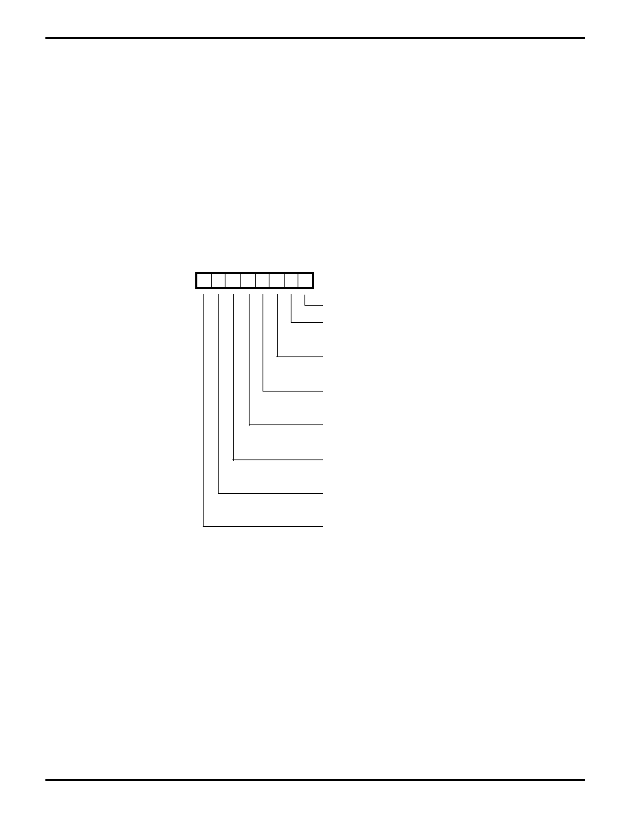
86
P R E L I M I N A R Y
Z80185/Z80195
S
MART
P
ERIPHERAL
C
ONTROLLERS
DS971850301
Zilog
Individual Pin Selection Between PIA1 and
CTCs
The assignment of the choice between PIA1 and CTC I/Os
is controlled by the PIA1/CTC Pin Select Register (Figure
79).
Bit 7.
Reserved, and should be programmed as 0.
Bits 6-4.
When the PIA1 data direction register has set the
corresponding pins as outputs, for each of these bits that
is 0, the pin is driven with the state of the corresponding bit
of the PIA 1 Data register, while for each of these bits that
is 1, the associated pin is driven with the indicated CTC
output. These bits Reset to 0.
Bits 3-1.
These bits control whether the CLK/TRG inputs of
CTCs 3-1 are taken from PIA3-1, respectively, or from the
ZC/TO outputs of CTC2-0, respectively. These bits do not
have any affect on the operating mode of the CTCs.
Bit 0.
This bit is reserved and should be programmed as
0. CTC0's CLK/TRG0 input is always connected to the
PIA10 pin.
0
0
0
0
0
0
0
0
PIA1/CTC Pin Select Register (I/O Address %DE)
7
6
5
4
3
2
1
0
Reserved, program as 0.
Reserved, program as 0.
PIA11/CLKTRG1
1 = CLK/TRG1 = ZC/TO0
0 = CLK/TRG1 = pin
PIA12/CLKTRG2
0 = CLK/TRG2 = ZC/TO1
1 = CLK/TRG2 = pin
PIA13/CLKTRG3
0 = CLK/TRG3 = ZC/TO2
1 = CLK/TRG3 = pin
PIA14/ZCTO1
0 = PIA14
1 = ZC/TO1
PIA15/ZCTO2
0 = PIA15
1 = ZC/TO2
PIA16/ZCTO3
0 = PIA16
1 = ZC/TO3
PIA16/ZCTO3
0 = PIA16
1 = ZC/TO3
Figure 88. PIA1/CTC Pin Select Register
(I/O Address %DE)

87
P R E L I M I N A R Y
Z80185/Z80195
S
MART
P
ERIPHERAL
C
ONTROLLES
DS971850301
Zilog
Z80185 PIA AND MISCELLANEOUS REGISTERS
(Continued)
CTC Control Registers
Channel Control Byte
This byte is used to set the operating modes and param-
eters. Bit D0 must be a 1 to indicate that this is a Control
Byte (Figure 82).
The Channel Control Byte register has the following fields:
Bit D7.
Interrupt Enable. This bit enables the interrupt logic
so that an internal INT is generated at zero count. Interrupts
are programmed in either mode, and may be enabled or
disabled at any time.
Bit D6.
Mode Bit. This bit, along with bit 3, is used to select
either Timer mode or Counter mode (Table 8).
Bit D5.
Prescaler Factor. This bit selects the prescaler
factor for use in the timer mode. Either divide-by-16 or
divide-by-256 is available.
Bit D4.
Clock/Trigger Edge Selector. This bit selects the
active edge of the CLK/TRG input pulses.
Bit D3.
Mode Bit. This bit, along with bit 6, selects either
Timer mode or Counter mode (Table 8).
Bit D2.
Time Constant. This bit indicates that the next byte
programmed is time constant data for the downcounter.
Bit D1.
Software Reset. Writing a 1 to this bit indicates a
software reset operation, which stops counting activities
until another time constant word is written.
Table 8. CTC Operation Modes
CCW6
CCW3
Operation
0
0
(Auto Start) Timer mode. The
prescaler is clocked by PHI, and the
counter is clocked by the prescaler.
Counting is enabled when the timer
constant is loaded.
0
1
Timer with CLK/TRG Trigger. The
prescaler is clocked by PHI, and the
counter is clocked by the prescaler.
Timing starts when the transition
specified by D4 is detected on the
PIA pin, or for CTC3-1, the ZC/T0
output of CTC2-0, respectively.
1
0
Classic Counter mode. The counter
is clocked by the PIA pin, or for
CTC3-1 the ZC/TO output of
CTC-2 respectively.
1
1
Long Counter mode. The prescaler
is clocked by the PIA pin, or for
CTC3-1 the ZC/TO output of
CTC-2, respectively, and the
counter is clocked by the prescaler.
88
P R E L I M I N A R Y
Z80185/Z80195
S
MART
P
ERIPHERAL
C
ONTROLLERS
DS971850301
Zilog
D7
D6
D5
D4
D3
D2
D1
D0
Control or Vector
0 Vector
1 Control Word
Reset
0 Continued Operation
1 Software Reset
Time Constant
0 No Time Constant Follows
1 Time Constant Follows
Mode
CCW6 CCW3
0 0 Timer Mode (Auto Start)
0 1 Timer Mode CLK/TRG Pulse Starts
1 0 Classic Counter Mode
1 1 Long Counter Mode
Interrupt
1 Enables Interrupt
0 Disables Interrupt
Prescaler Value
1 Value of 256
0 Value of 16
CLK/TRG Edge Selection
0 Selects Falling Edge
1 Selects Rising Edge
Addr: E4h (Ch 0)
E5h (Ch 1)
E6h (Ch 2)
E7h (Ch 3)
Figure 89. CTC Channel Control Word

89
P R E L I M I N A R Y
Z80185/Z80195
S
MART
P
ERIPHERAL
C
ONTROLLES
DS971850301
Zilog
Z80185 PIA AND MISCELLANEOUS REGISTERS
(Continued)
CTC Control Registers
(Continued)
Time Constant
Before a channel can start counting, it must receive a time
constant. The time constant value may be anywhere be-
tween 1 and 256, with 0 indicating a count of 256 (Figure
90).
D7 D6 D5 D4 D3 D2 D1 D0
TC0
TC1
TC2
TC3
TC4
TC5
TC6
TC7
Figure 90. CTC Time Constant
Interrupt Vector
If one or more of the CTC channels have interrupt enabled,
then the Interrupt Vector Word should be programmed.
Only the five most significant bits of this word are used, bit
D0 must be 0 . Bits D2-D1 are automatically modified by
the CTC channels after responding with an interrupt vector
(Figure 91).
D7 D6 D5 D4 D3 D2 D1 D0
0 Interrupt Vector Register
1 Control Register
Channel Identifier
(Automatically Inserted by CTC)
0 0 Channel 0
0 1 Channel 1
1 0 Channel 2
1 1 Channel 3
Supplied By User
Figure 91. CTC Interrupt Vector
Watch-Dog Timer
The Z80185's Watch-Dog Timer (WDT) facility is identical
to Zilog's Z84C15 WDT with the following exceptions:
1. The HALT mode field of the WDT Master Register is not
used. Power control is handled as on the Z8S180.
2. Rather than having a separate /WDTOUT output pin,
the output of the WDT is logically Low-active-ORed with
the /RESET pin. A new register bit controls whether this
affects only the processor, by means of an internal logic
gate, or whether it also drives the /RESET pin Low in an
open-drain manner, so that external logic can be Reset
by the WDT as well. The latter is the default state after
power-up or Reset.

90
P R E L I M I N A R Y
Z80185/Z80195
S
MART
P
ERIPHERAL
C
ONTROLLERS
DS971850301
Zilog
Watch-Dog Control Registers
Two registers control WDT operations. These are WDT
Master Register (WDTMR; I/O Address F0h) and the WDT
Command Register (WDTCR; I/O Address F1h). WDT
logic has a "double key" structure to prevent accidental
disabling of the WDT.
Enabling the WDT.
The WDT is enabled by reset, and
setting the WDT Enable Bit (WDTMR7) to 1.
Disabling the WDT.
The WDT is disabled by clearing WDT
Enable bit (WDTR7) to 0 followed by writing "B1h" to the
WDT Command Register (WDTCR; I/O Address F1h).
Clearing the WDT.
The WDT can be cleared by writing
"4Eh" into the WDTCR.
Watch-Dog Timer Master Register (WDTMR;I/O ad-
dress F0h).
This register controls the activities of the
Watch-Dog Timer.
Bit D7.
Watch-Dog Timer Enable (WDTE). The WDT can be
enabled by setting this bit to 1. To disable WDT, write 0 to
this bit, followed by writing "B1h" to the WDT Command
Register. Upon Power-On Reset, this bit is set to 1 and the
WDT is enabled.
Bit D6-D5.
WDT Periodic field (WDTP). This 2-bit field
determines the desired time period. Upon Power-on reset,
this field sets to "11".
00 - Period is (TcC * 2
16
)
01 - Period is (TcC * 2
18
)
10 - Period is (TcC * 2
20
)
11 - Period is (TcC * 2
22
)
Bit D4.
If this bit is 1 and the WDT times out, the Z80185
drives the /Reset pin Low to reset external logic. If this bit
is 0, a WDT timer only resets the Z80185 internally.
Bit D3-D0.
Reserved. These three bits are reserved and
should always be programmed as 0011. Reading these
bits returns 0011.
1
1
1
1
0
0
1
1
Should be 0011
7
6
5
4
3
2
1
0
Drive /RESET
0 = WDT output only resets 185
1 = Output of WDT is driven
onto /RESET pin
WDT Periodic Field
00 = Period is (TcC X 2*16)
01 = Period is (TcC X 2*18)
10 = Period is (TcC X 2*20)
11 = Period is (TcC X 2*22)
Watch-Dog Timer Enable
0 = Disable
1 = Enable
Figure 92. Watch-Dog Timer Master Register
(I/O Address %F0)
Watch-Dog Timer Command Register
(WDTCR; I/O
Address F1h). This register is Write Only (Figure 93).
Write B1h after clearing WDTE to "0" - Disable WDT
Write 4Eh - Clear WDT
D7
D6
D5
D4
D3
D2
D1
D0
(B1h) - Disable WDT
(After Clearing WDTE)
1
0
0
1
1
0
1
0
0
1
0
1
0
1
1
0
(4Eh) - Clear WDT to zero
WDTCR (Write Only)
Figure 93. Watch-Dog Timer Command Register

91
P R E L I M I N A R Y
Z80185/Z80195
S
MART
P
ERIPHERAL
C
ONTROLLES
DS971850301
Zilog
Z80185 PIA AND MISCELLANEOUS REGISTERS
(Continued)
Parallel Ports
The Z80185 has two 8-bit bidirectional ports. Each bit is
individually programmable for input or output. Each port
includes two registers: the Port Direction Control Register
and the Port Data Register. The second port also includes
an Alternate Address that is used with the Bidirectional
Centronics feature.
1
1
1
1
1
1
1
1
PIA 1 Data Direction Register
0 = Output
1 = Input
7
6
5
4
3
2
1
0
0
0
0
0
0
0
0
0
PIA 1 Data Register
7
6
5
4
3
2
1
0
0
0
0
0
0
0
0
0
PIA 2 Data Register
7
6
5
4
3
2
1
0
0
0
0
0
0
0
0
0
PIA 2 Data Register
7
6
5
4
3
2
1
0
0
0
0
0
0
0
0
0
PIA 2 Data Register
7
6
5
4
3
2
1
0
Figure 94. PIA 1 Data Direction Register
(I/O Address %E0)
The data direction register determines which of the PIA16-
10 pins are inputs and outputs. When a bit is set to 1, the
corresponding bit in the PIA 1 Data Register is an input. If
the bit is 0, then the corresponding pin is an output. These
bits must be set appropriately if these pins are used for
CTC inputs and outputs.
Figure 95. PIA 1 Data Register
(I/O Address %E1)
When the processor writes to the PIA 1 Data Register, the
data is stored in the internal buffer. Any bits that are output
are then driven on to the pins.
When the processor reads the PIA 1 Data Register, the
data on the external pins is returned.
Figure 96. PIA 2 Data Direction Register
(I/O Address %E2)
The data direction register determines which of the PIA27-
20 pins are inputs and outputs. When a bit is set to a 1, the
corresponding pin is an input. If the bit is 0, then the
corresponding bit is an output. These settings can be
overridden by the Bidirectional Centronics Controller.
Figure 97. PIA 2 Data Register
(I/O Address %E3)
When the processor writes to the PIA 2 Data Register, the
data is stored in the internal buffer. Any bits that are output
are then driven on to the pins. In certain modes of the
Bidirectional Centronics Controller, an intermediate regis-
ter called the Output Holding Register is activated, and the
transfer of data from the OHR to the pins is under the
control of the controller.
When the processor reads the PIA 2 Data Register, the
data on the external pins is returned. In certain modes of
the Bidirectional Centronics Controller, reading from this
address reads the data stored in the port register from
PIA27-20 under the control of the controller.
Figure 98. PIA 2 Data Alternate Address
(RW) (I/O Address %EE)
Reading and writing this register is exactly the same as
reading and writing address E3 as described above,
except that in certain modes of the Bidirectional Centronics
Controller, writing to this address sets a "ninth bit" in the
opposite sense from writing address E3, and this drives
one of the control outputs with the opposite polarity.

92
P R E L I M I N A R Y
Z80185/Z80195
S
MART
P
ERIPHERAL
C
ONTROLLERS
DS971850301
Zilog
ELECTRICAL CHARACTERISTICS
The following classification table describes pins in terms of
input and output classes. V
DD
= 5V
±
10%, unless otherwise
noted.
Pin Input/Output Classification
Class "O" output:
Full time / totem pole
V
OL
0.4V max at I
OL
= 2.0 mA
V
OH
= V
DD
≠1.2V min at I
OH
= 200
µ
A
Slew rate 0.33 V/ns min at C
LOAD
= 50 pF
C
OUT
= 15 pF max (output or I/O)
Class "3" output:
as "O" except tri-state.
Class "H" output:
as "O" except V
OH
= V
DD
-0.6V min at I
OH
= 200
µ
A
Class "D" output:
Open Drain
V
OL
0.4V max at I
OL
= 12 mA
C
OUT
= 15 pF max (output or I/O)
Class "T" output:
Tri-State
As Class "O" at V
DD
= 3.3V
±
10%
V
OL
0.4V max at I
OL
= 12 mA, V
DD
= 5V
±
10%
V
OH
2.4V min at I
OH
= 12 mA, V
DD
= 5V
±
10%
Output impedance 45 ohms max
Slew rate 0.05 - 0.40 V/ns (C
LOAD
not stated by IEEE)
C
OUT
=15 pF max (output or I/O)
Class "I" input":
V
IL
0.8V max at V
DD
= 5V
±
10%
V
IL
0.6V max at V
DD
= 3.3V
±
10%
V
IH
2.0V min
Ii
±
10
µ
A max, Vi = 0 to 5V (includes leakage if I/O)
C
IN
= 5 pF max (if input only, see output type if I/O)
Inputs of this type include Weak Latch circuits.
Class "R" input:
V
IL
0.6V max
V
IH
V
DD
-0.6 min at V
DD
= 5V
±
10%
V
IH
V
DD
-0.3 min at V
DD
= 3.3V
±
10%
Ii
±
10
µ
A max, Vi = 0 to 5V
C
IN
= 5 pF max
Class "S" input:
V
IL
0.8V max at V
DD
= 5V
±
10%
V
IL
0.6V max at V
DD
= 3.3V
±
10%
V
IH
2.0V min
Hysteresis 0.2V min
Ii
±
20
µ
A max, Vi=0.8 to 2V (includes leakage if I/O)
Inputs of this type include Weak Latch circuits.

93
P R E L I M I N A R Y
Z80185/Z80195
S
MART
P
ERIPHERAL
C
ONTROLLES
DS971850301
Zilog
ELECTRICAL CHARACTERISTICS
(Continued)
The following table shows the characteristics of each pin
in terms of the above classifications. A dash "≠" in the input
or output column indicates the pin does not have that
function.
Pin
Input Class
Output Class
/BUSREQ
I
≠
/CTS
I
≠
/CTS0/RxS
I
≠
/DCD
I
≠
/DCD0/CKA1
I
3
/DTR
≠
O
/HALT
≠
O
/INT0
I
D
/INT1
I
≠
/INT2
I
≠
/IOCS
≠
O
/IORQ
I
3
/M1
I
3
/MREQ
I
3
/NMI
R
≠
/RAMCS
≠
O
/RD
I
3
/RESET
R
D
/RFSH
≠
O
/ROMCS
≠
O
/RTS
≠
O
/RTS0/TxS
≠
O
/RTXC
I
3
/TRXC
I
3
/WAIT
I
D
/WR
I
3
A0-A19
I
3
Pin
Input Class
Output Class
Busy
S
T
CKA0/CKS
I
3
D0-D7
I
3
EXTAL
R
≠
IEI
I
≠
IEO
≠
O
nAck
S
T
nAutoFd
S
T
nFault
S
T
nInit
S
T
nSelectIn
S
T
nStrobe
S
T
PError
S
T
PHI
≠
H
PIA13-10/CLKTRG3-0
I
3
PIA15-13/ZCTO2-0
I
3
PIA27-20
S
T
RXA0
I
≠
RXA1
I
≠
RXD
I
≠
/ST
≠
O
Select
S
T
TOUT//DREQ
I
O
TXA0
≠
O
TXA1
≠
O
TXD
≠
O
XTAL
≠
O
Table 9. Pin Classification Characteristics
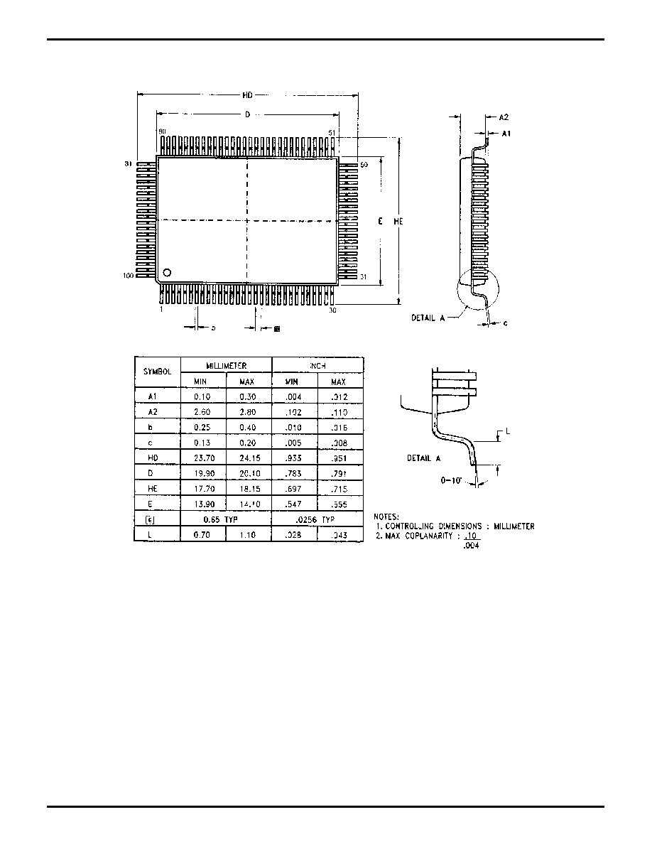
94
P R E L I M I N A R Y
Z80185/Z80195
S
MART
P
ERIPHERAL
C
ONTROLLERS
DS971850301
Zilog
PACKAGE INFORMATION
100-Pin QFP Package Diagram

95
P R E L I M I N A R Y
Z80185/Z80195
S
MART
P
ERIPHERAL
C
ONTROLLES
DS971850301
Zilog
ORDERING INFORMATION
Z80185 (ROM Version)
20 MHz
33 MHz
Z8018520FSC
Z8018533FSC
Z80195 (ROMless Version)
20 MHz
33 MHz
Z8019520FSC
Z8019533FSC
For fast results, contact your local Zilog sales office for
assistance in ordering the part(s) desired.
Package:
F = Plastic Quad Flatpack
Temperature:
S = 0
∞
C to +70
∞
C
Speeds:
20 = 20 MHz
33 = 33 MHZ
Environmental:
C = Plastic Standard
Example:
Z 80185 20 F S C
is a Z80185, 20 MHz, QFP, 0
∞
C to +70
∞
C, Plastic Standard Flow
Environmental Flow
Temperature
Package
Speed
Product Number
Zilog Prefix
Zilog's products are not authorized for use as critical compo-
nents in life support devices or systems unless a specific written
agreement pertaining to such intended use is executed between
the customer and Zilog prior to use. Life support devices or
systems are those which are intended for surgical implantation
into the body, or which sustains life whose failure to perform,
when properly used in accordance with instructions for use
provided in the labeling, can be reasonably expected to result in
significant injury to the user.
Zilog, Inc. 210 East Hacienda Ave.
Campbell, CA 95008-6600
Telephone (408) 370-8000
Telex 910-338-7621
FAX 408 370-8056
Internet: http://www.zilog.com
© 1997 by Zilog, Inc. All rights reserved. No part of this document
may be copied or reproduced in any form or by any means
without the prior written consent of Zilog, Inc. The information in
this document is subject to change without notice. Devices sold
by Zilog, Inc. are covered by warranty and patent indemnification
provisions appearing in Zilog, Inc. Terms and Conditions of Sale
only. Zilog, Inc. makes no warranty, express, statutory, implied or
by description, regarding the information set forth herein or
regarding the freedom of the described devices from intellectual
property infringement. Zilog, Inc. makes no warranty of mer-
chantability or fitness for any purpose. Zilog, Inc. shall not be
responsible for any errors that may appear in this document.
Zilog, Inc. makes no commitment to update or keep current the
information contained in this document.