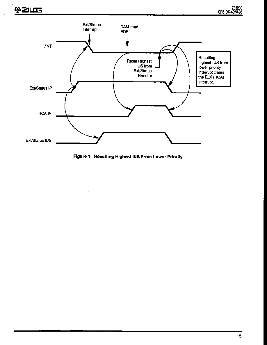
1
Z85233
CPS DC-4058-03
C
USTOMER
P
ROCUREMENT
S
PECIFICATION
GENERAL DESCRIPTION
The Zilog Enhanced Mono Serial Communication Controller,
Z85233 EMSCC, is a software compatible CMOS member
of the SCC family introduced by Zilog in 1981. The EMSCC
is a full-duplex data communications controller capable of
supporting a wide range of popular protocols. The Z85233
EMSCC is a single channel version (Channel A) of Zilog's
Z85230 ESCC. Based on ZIlog's unique Superintegration
TM
Technology, the EMSCC is compatible with designs using
Zilog's SCC and ESCC to receive and transmit data. It has
many improvements that significantly reduce CPU
overhead. The addition of a 4-byte transmit FIFO and an
8-byte receive FIFO significantly reduces the overhead
required to provide data to, and get data from, the transmitter
and receiver.
The EMSCC also has many features that improve packet
handling in SDLC mode. The EMSCC will automatically:
transmit a flag before the data, reset the Tx Underrun/EOM
latch, force the TxD pin high at the appropriate time when
using NRZI encoding, deassert the /RTS pin after the
closing flag, and better handle ABORTed frames when
using the 10x19 status FIFO. The combination of these
features along with the deeper data FIFOs significantly
simplifies SDLC driver software.
The CPU hardware interface has been simplified by reliev-
ing the databus setup time requirement and supporting
the software generation of the interrupt acknowledge
signal (/INTACK). These changes allow an interface with
less external logic to many microprocessor families while
maintaining compatibility with existing designs. I/O han-
dling of the EMSCC is improved over the SCC with faster
response of the /INT and /DTR//REQ pins.
The many enhancements added to the EMSCC permits a
system design that increases overall system performance
with better data handling and less interface logic.
Notes:
All Signals with a preceding front slash, "/", are active Low, e.g.:
B//W (WORD is active Low); /B/W (BYTE is active Low, only).
Power connections follow conventional descriptions below:
Connection
Circuit
Device
Power
V
CC
V
DD
Ground
GND
V
SS
Z85233
EMSCC
TM
E
NHANCED
M
ONO
S
ERIAL
C
OMMUNICATION
C
ONTROLLER
DC 4058-03
(11-4-94)

2
Z85233
CPS DC-4058-03
PIN DESCRIPTIONS
/INT
D7
D5
D3
D1
D0
D2
D4
D6
/RD
/WR
GND
/DTR/REQA
/RTSA
/CTSA
/DCDA
PCLK
NC
NC
NC
NC
NC
NC
/CE
D//C
NC
GND
NC
NC
NC
NC
NC
NC
IEO
IEI
/INTACK
VCC
/W//REQA
/SYNCA
/RTxCA
RxDA
/TRxCA
TxDA
GND
34
35
36
37
38
39
40
41
42
43
44
21
20
19
18
17
16
15
14
13
12
22
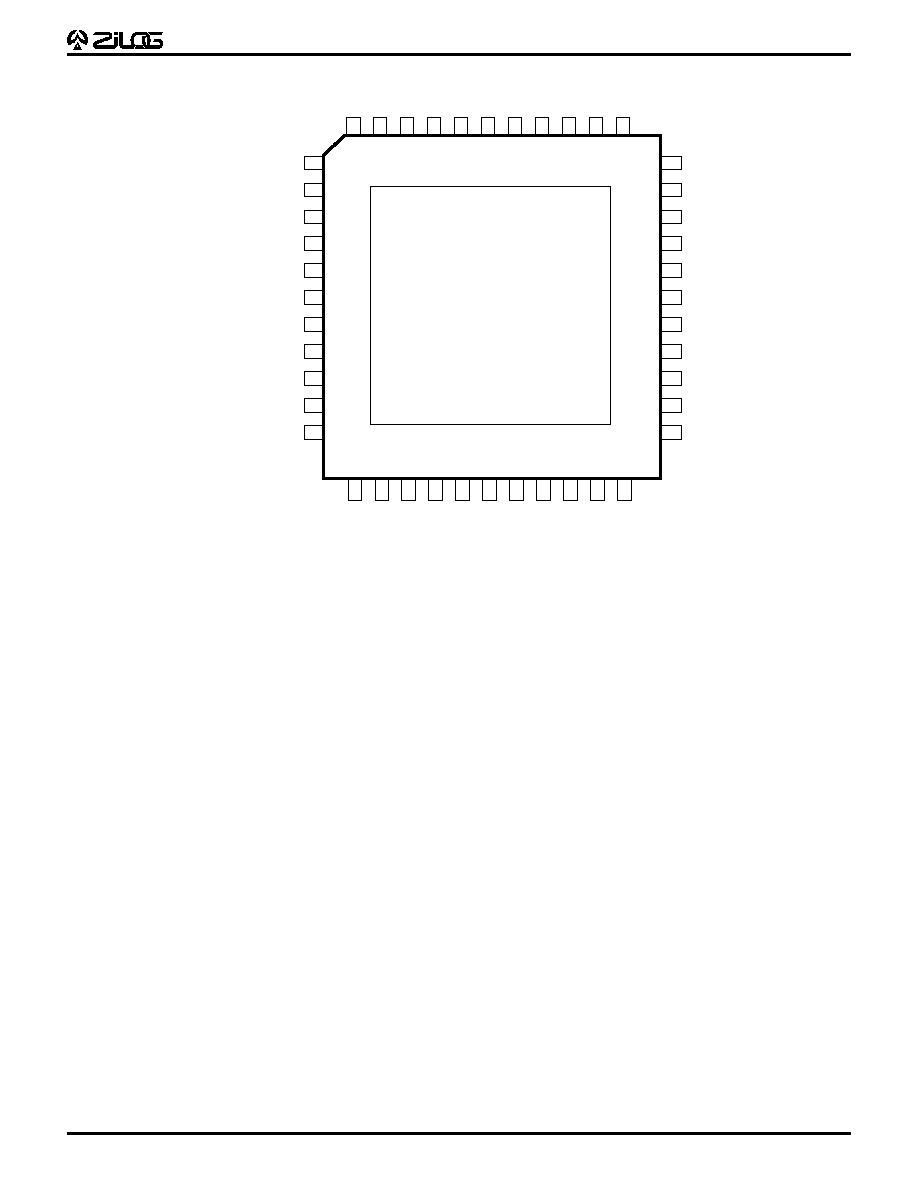
Z85233
(Top View)
33 32 31 30 29 28 27 26 25 24 23
1
2
3
4
5
6
7
8
9
10 11
Z85233 PQFP Pin Assignments
3
Z85233
CPS DC-4058-03
GND
/DTR//REQA
/RTSA
/CTSA
/DCDA
PCLK
NC
/IN
T
D7
D5
D3
D0
D2
D4
D6
/R
D
/W
R
D1
6
IEO
IEI
/INTACK
VCC
/W//REQA
/SYNCA
/RTxCA
RxDA
/TRxCA
TxDA
GND
NC
/CE
D//C
NC
GND
NC
NC
NC
NC
NC
NC
5
4
3
2
1
44 43 42 41 40
18 19 20 21 22 23 24 25 26 27 28
7
8
9
10
11
12
13
14
15
16
17
39
38
37
36
35
34
33
32
31
30
29
Z85233
(Top View)
NC
NC
NC
NC
Z85233 PLCC Pin Assignments

4
Z85233
CPS DC-4058-03
STANDARD TEST CONDITIONS
The DC Characteristics and capacitance sections below
apply for the following standard test conditions, unless
otherwise noted. All voltages are referenced to GND.
Positive current flows into the referenced pin.
Standard conditions are as follows:
s
+4.50 V
V
CC
+ 5.50 V
s
GND = 0 V
s
T
A
as specified in Ordering Information
From Output
Under Test
+5V
100 pF
250
�
A
2.1 k
ABSOLUTE MAXIMUM RATINGS
V
CC
Supply Voltage range ......................... -0.3V to +7.0V
Voltages on all pins
with respect to GND .......................... -0.3V to V
CC
+0.3V
Operating Ambient
Temperature ............................ See Ordering Information
Storage Temperature ............................ -65
�
C to +150
�
C
Stresses greater than those listed under Absolute Maxi-
mum Ratings may cause permanent damage to the de-
vice. This is a stress rating only; operation of the device at
any condition above those indicated in the operational
sections of these specifications is not implied. Exposure to
absolute maximum rating conditions for extended periods
may affect device reliability.
From Output
+5V
50 pF
2.2 k
Standard Test Load
Open-Drain Test Load
CAPACITANCE
Symbol
Parameter
Min
Max
Unit
Test Condition
C
IN
Input Capacitance
10
pF
Unmeasured pins
C
OUT
Output Capacitance
15
pF
returned to ground.
C
I/O
Bidirectional Capacitance
20
pF
Note:
f = 1 MHz, over specified temperature range.
MISCELLANEOUS
Gate Count - 7000

5
Z85233
CPS DC-4058-03
DC CHARACTERISTICS
Z85233
Symbol
Parameter
Min
Typ
Max
Unit
Condition
V
IH
Input High Voltage
2.2
V
CC
+0.3
V
V
IL
Input Low Voltage
-0.3
0.8
V
V
OH1
Output High Voltage
2.4
V
I
OH
= -1.6 mA
V
OH2
Output High Voltage
V
CC
-0.8
V
I
OH
= -250
�
A
V
OL
Output Low Voltage
0.4
V
I
OL
= + 2.0 mA
I
IL
Input Leakage
�
10.0
�
A
0.4< V
IN
<+2.4V
I
OL
Output Leakage
�
10.0
�
A
0.4< V
OUT
<+2.4V
I
CC1
V
CC
Supply Current
4
8 (10 MHz)
mA
V
CC
=5V V
IH
=4.8 V
IL
=0.2V
5
10 (16 MHz)
mA
Crystal Oscillators off
I
CC(OSC)
Crystal OSC Current
6
mA
Current for each osc.
in addition to I
CC1
Notes:
[1] V
CC
= 5V
�
10% unless otherwise specified, over specified temperature range.
[2] Typical I
CC
was measured with oscillator off.
[3] No I
CC
(osc) max is specified due to dependency on the external circuit.

6
Z85233
CPS DC-4058-03
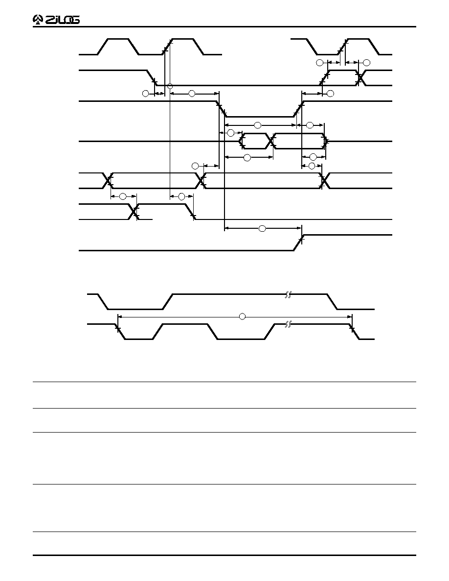
AC CHARACTERISTICS
Z85233 Read and Write Timing Diagram
PCLK
A//B, D//C
/INTACK
/CE
/RD
D7-D0
Read
Active
Valid
1
2
3
4
6
5
8
10
13
11
9
7
10
14
12
15
16
18
21
20
22
19
23
27
25
24
26
17
/WR
D7-D0
Write
28
30
31
29
/W//REQ
Wait
/W//REQ
Request
/DTR//REQ
Request
/INT
32
35
36
33
34
37
Read and Write Timing Diagram
/WR
/RD
47
48
46
Reset Timing Diagram
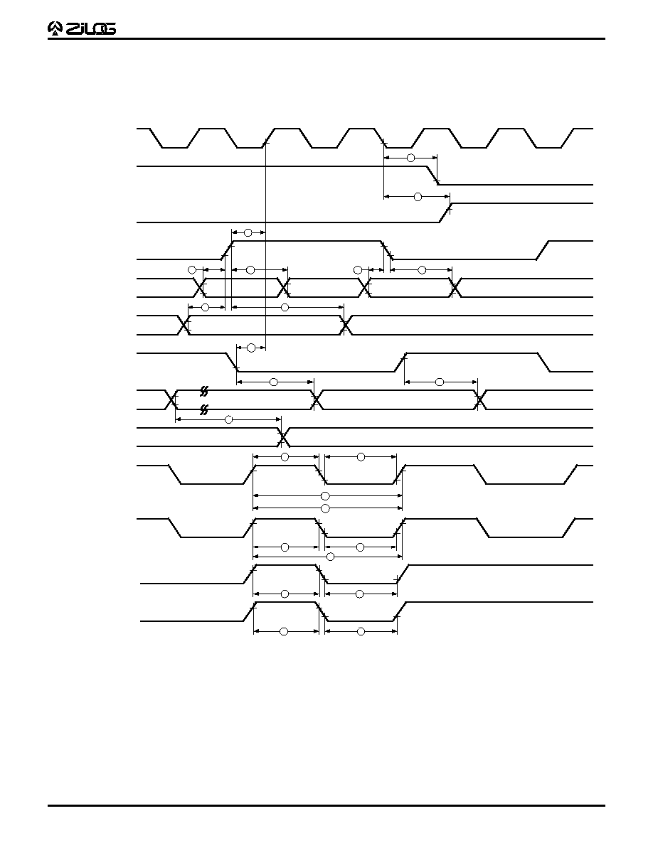
7
Z85233
CPS DC-4058-03
Active
Valid
PCLK
/INTACK
/RD
D7-D0
IEI
IEO
/INT
10
38
14
10
15
24
39
23
40
26
42
41
44
43
45
Interrupt Acknowledge Timing Diagram
/CE
/RD or /WR
49
Cycle Timing Diagram
AC CHARACTERISTICS
Z85233 Read and Write Timing Table
10 MHz 16 MHz
No
Symbol
Parameter
Min
Max
Min
Max
Notes
1
TwPCl
PCLK Low Width
40
1000
26
1000
2
TwPCh
PCLK High Width
40
1000
26
1000
3
TfPC
PCLK Fall Time
10
5
4
TrPC
PCLK Rise Time
10
5
5
TcPC
PCLK Cycle Time
100
2000
61
2000
6
TsA(WR)
Address to /WR Fall Setup Time
50
35
7
ThA(WR)
Address to /WR Rise Hold Time
0
0
8
TsA(RD)
Address to /RD Fall Setup Time
50
35
9
ThA(RD)
Address to /RD Rise Hold Time
0
0
10
TsIA(PC)
/INTACK to PCLK Rise Setup Time
20
15

8
Z85233
CPS DC-4058-03
AC CHARACTERISTICS
Z85233 Read and Write Timing Table
10 MHz 16 MHz
No
Symbol
Parameter
Min
Max
Min
Max
Notes
11
TsIAi(WR)
/INTACK to /WR Fall Setup Time
130
70
[1]
12
ThIA(WR)
/INTACK to /WR Rise Hold Time
0
0
13
TsIAi(RD)
/INTACK to /RD Fall Setup Time
130
70
[1]
14
ThIA(RD)
/INTACK to /RD Rise Hold Time
0
0
15
ThIA(PC)
/INTACK to PCLK Rise Hold Time
30
15
16
TsCEI(WR)
/CE Low to /WR Fall Setup Time
0
0
17
ThCE(WR)
/CE to /WR Rise Hold Time
0
0
18
TsCEh(WR)
/CE High to /WR Fall Setup Time
50
30
19
TsCEI(RD)
/CE Low to /RD Fall Setup Time
0
0
[1]
20
ThCE(RD)
/CE to /RD Rise Hold Time
0
0
[1]
21
TsCEh(RD)
/CE High to /RD Fall Setup Time
50
30
[1]
22
TwRDI
/RD Low Width
125
2TcPC 70
2TcPC
[1]
23
TdRD(DRA)
/RD Fall to Read Data Active Delay
0
0
24
TdRDr(DR)
/RD Rise to Data Not Valid Delay
0
0
25
TdRDI(DR)
/RD Fall to Read Data Valid Delay
120
70
26
TdRD(DRz)
/RD Rise to Read Data Float Delay
35
30
27
TdA(DR)
Addr to Read Data Valid Delay
180
100
28
TwWRI
/WR Low Width
125
75
29
TdWR(DW)
/WR Fall to Write Data Valid Delay
20
20
30
ThDW(WR)
Write Data to /WR Rise Hold Time
0
0
31
TdWR(W)
/WR Fall to Wait Valid Delay
100
50
[4]
32
TdRD(W)
/RD Fall to Wait Valid Delay
100
50
[4]
33
TdWRf(REQ)
/WR Fall to /W//REQ Not Valid Delay
120
70
34
TdRDf(REQ)
/RD Fall to /W//REQ Not Valid Delay
120
70
[6]
35a
TdWRr(REQ)
/WR Fall to /DTR//REQ Not Valid
4TcPc
4TcPc
35b
TdWRr(REQ)
/WR Fall to /DTR//REQ Not Valid
100
70
[6]
36
TdRDr(REQ)
/RD Rise to /DTR//REQ Not Valid Delay
NA
NA
37
TdPC(INT)
PCLK Fall to /INT Valid Delay
320
175
38
TdIAi(RD)
/INTACK to /RD Fall (Ack) Delay
90
50
[5]
39
TwRDA
/RD (Acknowledge) Width
125
75
40
TdRDA(DR)
/RD Fall(Ack) to Read Data Valid Delay
120
70
41
TsIEI(RDA)
IEI to /RD Fall (Ack) Setup Time
95
50
42
ThIEI(RDA)
IEI to /RD Rise (Ack) Hold Time
0
0
43
TdIEI(IEO)
IEI to IEO Delay Time
90
45
44
TdPC(IEO)
PCLK Rise to IEO Delay
175
80
45
TdRDA(INT)
/RD Fall to /INT Inactive Delay
320
200
[4]
46
TdRD(WRQ)
/RD Rise to /WR Fall Delay for No Reset
15
10
47
TdWRQ(RD)
/WR Rise to /RD Fall Delay for No Reset
15
10
48
TwRES
/WR and /RD Low for Reset
100
75
49
Trc
Valid Access Recovery Time
4TcPc
4TcPc
[3]
Notes:
[1] Parameter does not apply to Interrupt Acknowledge transactions.
[3] Parameter applies only between transactions involving the EMSCC.
[4] Open-drain output, measured with open-drain test load.
[5] Parameter is system dependent. For any EMSCC in the daisy chain, TdIAi(RD) must be greater than the sum of TdPC(IEO) for the highest priority
device in the daisy chain. TsIEI(RDA) for the EMSCC and TdIEI(IEO) for each device separating them in the daisy chain.
[6] Parameter applies to enhanced Request mode only (WR7' D4=1)
9
Z85233
CPS DC-4058-03
AC CHARACTERISTICS
Z85233 General Timing Diagram
General Timing Diagram
PCLK
/W//REQ, /DTR//REQ
Request
/W//REQ
Wait
/RTxC, /TRxC
Receive
RxD
/SYNC
External
/TRxC, /RTxC
Transmit
TxD
/TRxC
Output
/RTxC
/TRxC
/CTS, /DCD
/SYNC
Input
1
2
3
4
5
6
7
9
8
10
11
12
13
14
15
16
17
18
19
20
21
21
22
22

10
Z85233
CPS DC-4058-03
AC CHARACTERISTICS
Z85233 General Timing Table (Preliminary)
10 MHz 16 MHz
No
Symbol
Parameter
Min
Max
Min
Max
Notes
1a
TdPC(REQ)
/PCLK to W/REQ Valid
200
80
1b
TdPC(REQ)
/PCLK to DTR/ REQ Valid
200
80
[9]
2
TdPC(W)
/PCLK to Wait Inactive
300
180
3
TsRXC(PC)
/RxC to /PCLK Setup Time
NA
NA
NA
NA
[1,4]
4
TsRXD(RXCr)
RxD to /RxC Setup Time
0
0
[1]
5
ThRXD(RxCr)
RxD to /RXC Hold Time
125
50
[1]
6
TsRXD(RXCf)
RxD to /RXC Setup Time
0
0
[1,5]
7
ThRXD(RXCf)
RXD to /RXC Hold Time
125
50
[1,5]
8
TsSY(RXC)
/SYNC to /RxC Setup Time
-150
-100
[1]
9
ThSY(RXC)
/SYNC to/RXC Hold Time
5TcPc
5TcPc
[1]
10
TsTXC(PC)
/TxC to /PCLK Setup Time
NA
NA
[2,4]
11
TdTXCf(TXD)
/TxC to TxD Delay
150
80
[2]
12
TdTxCr(TXD)
/TxC to TxD Delay
150
80
[2,5]
13
TdTXD(TRX)
TxD to TRxC Delay
140
80
14
TwRTXh
RTxC High Width
120
80
[6]
15
TwRTXI
TRxC Low Width
120
80
[6]
16a
TcRTX
RTxC Cycle Time
400
244
[6,7]
16b
TxRX(DPLL)
DPLL Cycle Time Min
50
31
[7,8]
17
TcRTXX
Crystal Osc. Period
100
1000
61
1000
[3]
18
TwTRXh
TRxC High Width
120
80
[6]
19
TwTRXl
TRxC Low Width
120
80
[6]
20
TcTRX
TRxC Cycle Time
400
244
[6,7]
21
TwEXT
DCD or CTS Pulse Width
120
70
22
TwSY
SYNC Pulse Width
120
70
Notes:
[1] RxC is /RTxC or /TRxC, whichever is supplying the receive clock.
[2] TxC is /TRxC or /RTxC, whichever is supplying the transmit clock.
[3] Both /RTxC and /SYNC have 30 pF capacitors to ground connected to them.
[4] Synchronization of RxC to PCLK is eliminated in divide by four operation.
[5] Parameter applies only to FM encoding/decoding.
[6] Parameter applies only for transmitter and receiver; DPLL and baud rate generator timing requirements are identical to case PCLK requirements.
[7] The maximum receive or transmit data rate is 1/4 PCLK.
[8] Applies to DPLL clock source only. Maximum data rate of 1/4 PCLK still applies. DPLL clock should have a 50% duty cycle.
[9] Parameter applies only when WR7' D4 is set to '1'.
11
Z85233
CPS DC-4058-03
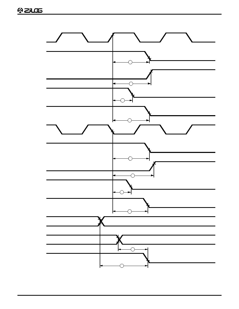
1
2
3
4
5
9
10
8
7
6
/RTxC, /TRxC
Receive
/W/REQ
Request
/W/REQ
Wait
/SYNC
Output
/INT
/RTxC, /TRxC
Transmit
/W//REQ
Request
/W//REQ
Wait
/DTR//REQ
Request
/INT
/CTS,
/DCD
/SYNC
Input
/INT
AC CHARACTERISTICS
Z85233 System Timing Diagram (Preliminary)
System Timing
12
Z85233
CPS DC-4058-03
AC CHARACTERISTICS
Z85233 System Timing Table (Preliminary)
10 MHz 16 MHz
No
Symbol
Parameter
Min
Max
Min
Max
Notes [4]
1
TdRXC(REQ)
/RXC to /W//REQ Valid
13
17
13
17
[2]
2
TdRXC(W)
/RxC to /Wait Inactive
13
17
13
17
[1,2]
3
TdRXC(SY)
/RxC to /SYNC Valid
4
7
4
7
[2]
4
TdRXC(INT)
/RxC to /INT Valid
15
21
15
21
[1,2]
5
TdTXC(REQ)
/TxC to /W//REQ Valid
11
14
11
14
[3]
6
TdTXC(W)
/TxC to /Wait Inactive
8
14
8
14
[1,3]
7
TdTXC(DRQ)
/TxC to /DTR//REQ Valid
9
12
9
12
[3]
8
TdTXC(INT)
/TxC to /INT Valid
5
9
5
9
[1,3]
9
TdSY(INT)
/SYNC to /INT Valid
2
7
2
7
[1]
10
TdEXT(INT)
/DCD or /CTS to /INT Valid
3
8
3
8
[1]
Notes:
[1] Open-drain output, measured with open-drain test load.
[2] /RxC is /RTxC or /TRxC, whichever is supplying the receive clock.
[3] /TxC is /TRxC or /RTxC, whichever is supplying the transmit clock.
[4] Units equal to TcPc