1
Z8614
CPS DC-4038-03
DESCRIPTION
DC 4038-03
(11-2-93)
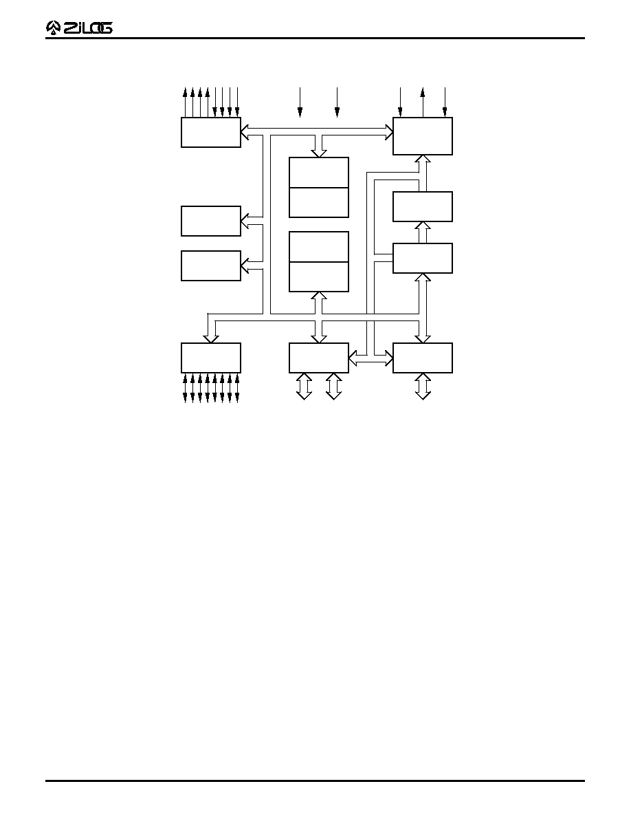
The Z8614 Keyboard Controller (KBC
TM
) introduces a new level
of sophistication to single-chip architecture. The Z8614 is a
member of the Z8 single-chip microcontroller family with 4
Kbytes of ROM.
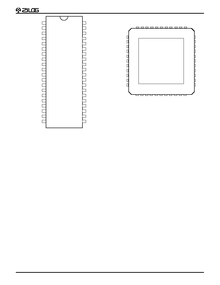
The Z8614 KBC is housed in 40-lead DIP and 44-lead PLCC
packages, and is manufactured in NMOS technology. Zilog's
microcontroller offers fast execution, efficient use of memory,
sophisticated interrupt, input/output bit manipulation capabili-
ties, and easy hardware/software system expansion along with
low cost and low power consumption.
The KBC architecture is characterized by a flexible I/O scheme,
an efficient register, I/O, and a number of ancillary features that
are useful in keyboard applications.
The device applications demand powerful I/O capabilities. The
KBC fulfills this with 32 pins dedicated to input and output.
These lines are grouped into four ports, each port consists of eight
lines, and are configurable under software control to provide
timing, status signals, and serial or parallel I/O ports.
The Z8614 offers low EMI emission achieved by means of
Z8614
K
EYBOARD
C
ONTROLLER (KBC
TM
)
NMOS Z8
Æ
8-BIT MCU
several modifications in the output drivers and clock circuitry of
the device.
There are two basic address spaces available to support this wide
range of configurations: Program Memory and 124 General-
Purpose Registers.
The KBC offers two on-chip counter/timers with a large number
of user selectable modes. This unburdens the program from
coping with real-time problems such as counting/timing.
Notes:
All Signals with a preceding front slash, "/", are active Low, e.g., B//W
(WORD is active Low); /B/W (BYTE is active Low, only).
Power connections follow conventional descriptions below:
Connection
Circuit
Device
Power
V
CC
V
DD
Ground
GND
V
SS
C
USTOMER
P
ROCUREMENT
S
PECIFICATION
3
Z8614
CPS DC-4038-03
1
2
3
4
5
6
7
8
9
10
11
12
13
14
15
16
17
18
19
20
Vcc
XTAL2
XTAL1
P37
P30
/RESET
N/C*
N/C*
N/C
P35
GND
P32
P00
P01
P02
P03
P04
P05
P06
P07
P36
P31
P27
P26
P25
P24
P23
P22
P21
P20
P33
P34
P17
P16
P15
P14
P13
P12
P11
P10
40
39
38
37
36
35
34
33
32
31
30
29
28
27
26
25
24
23
22
21
Z8614
DIP
Note: Pins 7 and 8 actually are connected to the chip,
although used only for testing. These pins must be
used as floaters by the customer.
40-Lead DIP Pin Configuration
Note: Pins 8 and 9 actually are connected to the chip,
although used only for testing. These pins must be
used as floaters by the customer.
N/C
P30
P37
XT
AL1
XT
AL2
VCC
P36
P31
P27
P26
P25
P03
P04
P05
P06
P07
P10
P1
1
P12
P13
P14
N/C
N/C
P24
P23
P22
P21
P20
P33
P34
P17
P16
P15
/RESET
N/C*
N/C*
N/C
P35
GND
P32
P00
P01
P02
NC
7
8
9
10
11
12
13
14
15
16
17
38
37
36
35
34
33
32
31
30
29
39
Z8614
PLCC
6
5
4
3
2
1
44 43 42 41 40
18 19 20 21 22 23 24 25 26 27 28
44-Lead PLCC Pin Configuration
4
Z8614
CPS DC-4038-03
Note:
* Typical @ 25
∞
C
1. A combined total of six I/O pins from Ports 2 and 3 may be used to sink 10 mA
at 0.8 V
OL
(max three pins per port). These may be used for LEDs or as general
purpose outputs requiring high sink current.
DC CHARACTERISTICS
V
CC
= 4.75 V to 5.25V @ 0
∞
C to +70
∞
C
Symbol
Parameter
Min
Max
Typ*
Unit
Condition
V
CH
Clock Input High Voltage
3.8
V
CC
V
Driven by External Clock Generator
V
CL
Clock Input Low Voltage
≠0.3
0.8
V
Driven by External Clock Generator
V
IH
Input High Voltage
2.0
V
CC
V
V
IL
Input Low Voltage
≠0.3
0.8
V
V
RH
Reset Input High Voltage
3.8
V
CC
V
V
RL
Reset Input Low Voltage
≠0.3
0.8
V
V
OH
Output High Voltage
2.0
V
I
OH
= ≠250
µ
A (Port 2 only)
Output High Voltage
2.4
V
I
OH
= ≠250
µ
A (Port 3 only)
V
OL
Output Low Voltage
0.8
V
I
OL
= +4.0 mA (see Note 1 below)
I
IL
Input Leakage
≠10
10
µ
A
V
IN
= 0V, 5.25V
I
OL
Output Leakage
≠10
10
µ
A
V
IN
= 0V, 5.25V
I
IR
Reset Input Current
≠50
µ
A
V
IN
= 0V, 5.25V
I
CC
V
CC
Supply Current
150
135
mA
Zilog's products are not authorized for use as critical components in life
support devices or systems unless a specific written agreement pertain-
ing to such intended use is executed between the customer and Zilog
prior to use. Life support devices or systems are those which are intended
for surgical implantation into the body, or which sustains life whose
failure to perform, when properly used in accordance with instructions
for use provided in the labeling, can be reasonably expected to result in
significant injury to the user.
Zilog, Inc. 210 East Hacienda Ave.
Campbell, CA 95008-6600
Telephone (408) 370-8000
Telex 910-338-7621
FAX 408 370-8056
© 1993 by Zilog, Inc. All rights reserved. No part of this document may
be copied or reproduced in any form or by any means without the prior
written consent of Zilog, Inc. The information in this document is subject
to change without notice. Devices sold by Zilog, Inc. are covered by
warranty and patent indemnification provisions appearing in Zilog, Inc.
Terms and Conditions of Sale only. Zilog, Inc. makes no warranty,
express, statutory, implied or by description, regarding the information
set forth herein or regarding the freedom of the described devices from
intellectual property infringement. Zilog, Inc. makes no warranty of
merchantability or fitness for any purpose. Zilog, Inc. shall not be
responsible for any errors that may appear in this document. Zilog, Inc.
makes no commitment to update or keep current the information
contained in this document.