 | –≠–ª–µ–∫—Ç—Ä–æ–Ω–Ω—ã–π –∫–æ–º–ø–æ–Ω–µ–Ω—Ç: Z8615 | –°–∫–∞—á–∞—Ç—å:  PDF PDF  ZIP ZIP |

1
Z8615
CPS DC-4143-05
DESCRIPTION
DC-4143-05
(5-13-94)
Z8615
NMOS Z8
Æ
8-BIT MCU
K
EYBOARD
C
ONTROLLER
C
USTOMER
P
ROCUREMENT
S
PECIFICATION
The Z8615 Keyboard Controller (KBC) is a member of the
Z8
Æ
single-chip microcontroller family with 4 Kbytes of
ROM. The device is housed in a 40-pin DIP and 44-pin
PLCC package, and is manufactured in NMOS technol-
ogy. The Z8615 KBC microcontroller offers fast execution,
efficient use of memory, sophisticated interrupt, input/
output bit-manipulation capabilities, and easy hardware/
software system expansion along with low cost and low
power consumption.
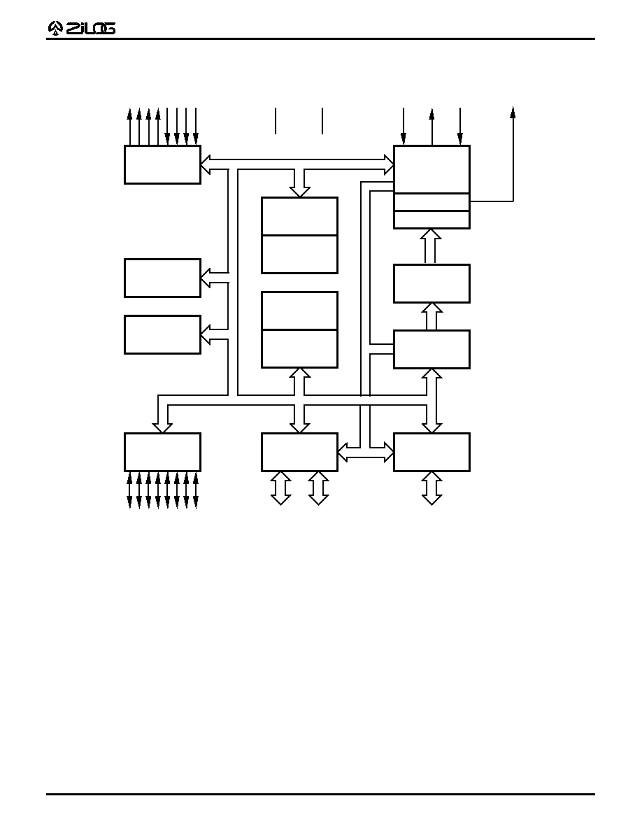
The Z8615 KBC architecture is characterized by a flexible
I/O scheme, an efficient register, I/O, and a number of
ancillary features that are useful in many industrial and
advanced scientific applications.
For applications which demand powerful I/O capabilities,
the KBC provides 32 pins dedicated to input and output.
These lines are grouped into four ports, each port consists
of 8 lines, and are configurable under software control to
provide timing, status signals, and serial or parallel I/O
ports.
The Z8615 KBC offers low EMI emission which is achieved
by means of several modifications in the output drivers and
clock circuitry of the device.
There are two basic address spaces which are available to
support this wide range of configurations: Program Memory
and 124 General-Purpose Registers.
The Z8615 KBC offers two on-chip counter/timers with a
large number of user-selectable modes. This unburdens
the program from coping with real-time problems such as
counting/timing (Block Diagram).
Notes:
All Signals with a preceding front slash, "/", are active Low, e.g.,
B//W (WORD is active Low); /B/W (BYTE is active Low, only).
Power connections follow conventional descriptions below:
Connection
Circuit
Device
Power
V
CC
V
DD
Ground
GND
V
SS
2
Z8615
CPS DC-4143-05
GENERAL DESCRIPTION
(Continued)
Functional Block Diagram
Port 3
Counter/
Timers (2)
Interrupt
Control
Port 2
I/O
(Bit Programmable)
ALU
Flags
Register
Pointer
Register File
124 x 8 Bit
Machine
Timing & Inst.
Control
Program
Memory
Program
Counter
Vcc
GND
XTAL1 XTAL2 /RESET
Output
Input
Port 0
Port 1
I/O
Output Open Drain
(Nibble Programmable)
I/O
Output Open Drain
(Byte Programmable)
4
4
8
WDT
/WDTOUT
POR
3
Z8615
CPS DC-4143-05
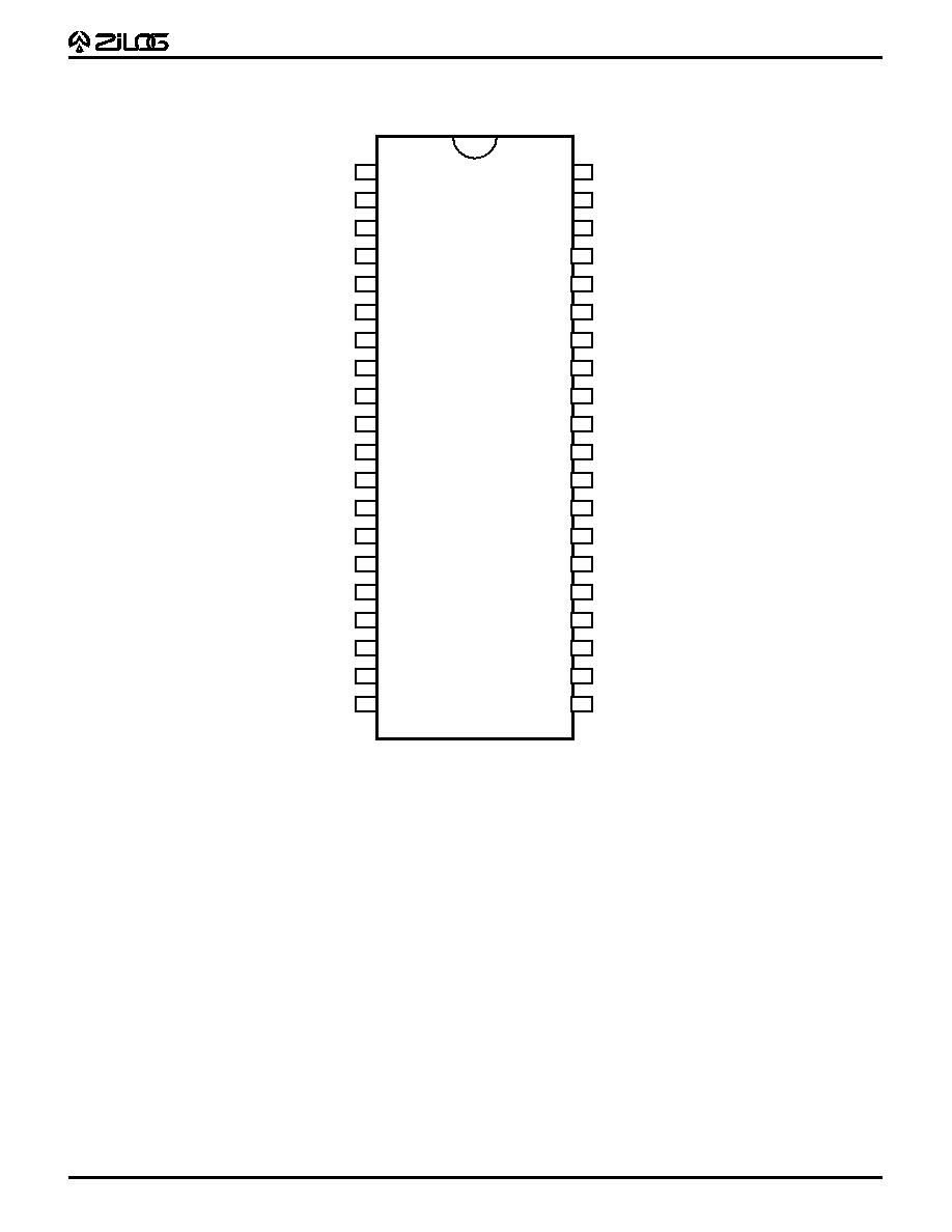
40-Pin Configuration
PIN IDENTIFICATION
*Note:
Pin 8 is connected to the chip, although used only for testing.
This pin must float. Pin 7 is a test pin and must be grounded.
1
2
3
4
5
6
7
8
9
10
11
12
13
14
15
16
17
18
19
20
VCC
XTAL2
XTAL1
P37
P30
/RESET
*GND
*NC
/WDTOUT
P35
GND
P32
P00
P01
P02
P03
P04
P05
P06
P07
P36
P31
P27
P26
P25
P24
P23
P22
P21
P20
P33
P34
P17
P16
P15
P14
P13
P12
P11
P10
40
39
38
37
36
35
34
33
32
31
30
29
28
27
26
25
24
23
22
21
Z8615
4
Z8615
CPS DC-4143-05
PIN IDENTIFICATION
(Continued)
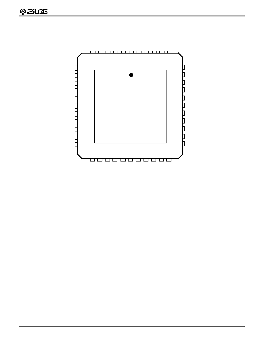
N/C
P30
P37
XT
AL1
XT
AL2
VCC
P36
P31
P27
P26
P25
P03
P04
P05
P06
P07
P10
P1
1
P12
P13
P14
N/C
N/C
P24
P23
P22
P21
P20
P33
P34
P17
P16
P15
/RESET
*GND
*N/C
/WDTOUT
P35
GND
P32
P00
P01
P02
N/C
7
8
9
10
11
12
13
14
15
16
17
38
37
36
35
34
33
32
31
30
29
39
Z8615
PLCC
6
5
4
3
2
1
44 43 42 41 40
18 19 20 21 22 23 24 25 26 27 28
Note:
* Pin 9 is connected to the chip, although used only for testing.
This pin must float. Pin 8 is a test pin and must be grounded.
44-Pin PLCC Pin Assignments

5
Z8615
CPS DC-4143-05
Stresses greater than those listed under Absolute Maxi-
mum Ratings may cause permanent damage to the de-
vice. This is a stress rating only; operation of the device at
any condition above those indicated in the operational
sections of these specifications is not implied. Exposure to
absolute maximum rating conditions for extended periods
may affect device reliability.
Notes:
* Voltage on all pins with respect to GND.
See ordering information
ABSOLUTE MAXIMUM RATINGS
Symbol
Description
Min
Max
Units
V
CC
Supply Voltage*
≠0.3
+7.0
V
T
STG
Storage Temp
≠65
+150
C
T
A
Oper Ambient Temp
STANDARD TEST CONDITIONS
The characteristics listed here apply for standard test
conditions as noted. All voltages are referenced to GND.
Positive current flows into the referenced pin (Test Load).
Test Load Diagram
STANDARD TEST CONDITIONS
T
A
= 25
∞
C, V
CC
= GND = 0V, f = 1.0 MHz, unmeasured pins returned to ground.
Parameter
Max
Input capacitance
12 pF
Output capacitance
12 pF
I/O capacitance
12 pF
From Output
Under Test
150 pF

6
Z8615
CPS DC-4143-05
DC CHARACTERISTICS
V
CC
= 4.75V to 5.25V @ 0
∞
C to -55
∞
C
Sym
Parameter
Min
Max
Typ*
Unit
Condition
V
CH
Clock Input High Voltage
3.8
V
CC
V
Driven by External Clock Generator
V
CL
Clock Input Low Voltage
≠0.3
0.8
V
Driven by External Clock Generator
V
IH
Input High Voltage
2.0
V
CC
V
V
IL
Input Low Voltage
≠0.3
0.8
V
V
RH
Reset Input High Voltage
3.8
V
CC
V
V
RL
Reset Input Low Voltage
≠0.3
0.8
V
V
OH
Output High Voltage
2.0
V
I
OH
= ≠250
µ
A (Port 2 only)
Output High Voltage
2.4
V
I
OH
= ≠250
µ
A (Port 3 only)
V
OL
Output Low Voltage
0.8
V
I
OL
= 10.0 mA (See note [1] below.)
I
IL
Input Leakage
≠10
1 0
µ
A
V
IN
= 0V, 5.25V (See note [3] below.)
I
OL
Output Leakage
≠10
1 0
µ
A
V
IN
= 0V, 5.25V (See note [2] below.)
I
IR
Reset Input Current
≠335
≠775
≠477
µ
A
V
IN
= 0V
I
R1
Input Current
≠335
≠775
µ
A
Pull-up resistor=10.4 Kohms, V
IN
=0.0V
I
R2
Input Current
≠1.6
≠2.9
mA
Pull-up resistor = 2.4 Kohms, V
IN
=0.0V
I
CC
V
CC
Supply Current
150
mA
WDT
Watch-Dog Timer
2.0
mA
V
OL
=0.4 Volt
Notes:
* Typical @ 25
∞
C
[1]
Ports P37-P34 may be used to sink 12 mA at 2.8V. These may be
used for LEDs or as general-purpose outputs requiring high sink
current.
[2]
P00-P07, P10-P17, P20-P25, P30-P33 as output mode open-drain
as a logic one.
[3]
P04-P07, P10-P17, P20-P23, P30-P33 as input mode.

7
Z8615
CPS DC-4143-05
TOLERANCE VALUES
The Z8615 provides internal pull-up resistors. Tolerances
for these resistors consists of the following:
Resistor
Tolerance
2.4K
±
25%
10.4K
±
35%
The RC Oscillator option provided on the Z8615 requires an
external 1% precision resistor. Tolerance for the oscillator
consists of the following:
Frequency:
4 MHz to 5 MHz
Tolerance:
+ 10%, ≠ 10%
Note:
1) All Characteristics stated above are specified
according to the following:
V
CC
= 4.75 to 5.25
Temperature = 15
∞
C to 55
∞
C
2) To measure the RC oscillator's frequency, use only a high-
impedance probe (10 Mohms, 2 pf) to probe XTAL2 (Pin 2). Other
probes with higher capacitance loading can create strong ground
bounces which shift the frequency reading at XTAL2. Also, do not
probe XTAL1 when measuring the RC frequency. Refer to the
procedure for Test Conditions and Methodology.
3) To measure the POR delay, apply a square wave (amplitude = 4
volts, frequency ~ .5 Hertz) to RESET (Pin 6) then measure the time it
takes for Data Strobe (Pin 8) to go high after RESET goes high. Refer
to the procedure for Test Conditions and Methodology.

8
Z8615
CPS DC-4143-05
TEST CONDITIONS AND METHODOLOGY
1.
Title:
Z08615CA UTB Frequency-POR Measurement
Procedure.
2.
Objective:
To provide instructions for making frequency and POR
measurements.
3.
Scope:
All products containing on-board RC oscillator.
4.
Applicable Documents:
4.1 Instruction manuals for H-P 8012B Pulse Generator,
H-P 1661A Logic Analyzer, Tektronix DC 503A
Universal Counter/Timer.
4.2 Data Sheet for device under test.
5.
Equipment, Materials, and Supplies:
5.1 One UTB (agreed upon by customer).
5.2 One DIN-5 (female) connector or PC (IBMÆ or
clone) to power the keyboard.
5.3 H-P 8012B Pulse Generator.
5.4 H-P 1661A Logic Analyzer.
5.5 Tektronix DC 503A Universal Counter/Timer and
Tektronix P6202A DC to 500 MHz 10 meg≠2 pico
probe.
5.6 H-P 6115A Precision Power Supply.
5.7 A temperature forcing unit (Temptronic
Corporation), or equivalent.
5.8 Golden correlation units.
6.
Important Notes:
6.1 The oscillator input/output is sensitive to external
loading, e.g., stray capacitance or inductance.
When making frequency measurement, make sure
the meter probe is on the oscillator output (Pin 2)
only (as close as possible). Any slight loading on
the oscillator input (Pin 3) will cause drastic changes
to the oscillator frequency. Therefore, it is
recommended that the RC resistor be connected
as close as possible to the oscillator input (Pin 3);
and that nothing is hanging on the oscillator input.
6.2 During frequency measurement, oscillator
input (Pin 3) should not be probed. The internal
circuitry requires that the external impedance on
this node be purely resistive. This is why the input
of the oscillator (Pin 3) is very sensitive to external
loading, then the frequency of the oscillator will be
unstable due to resonance (of loading) excited by
external, as well as internal noise.
To make a frequency reading, connect the scope
probe only to the oscillator out (Pin 2). Even though
this output is well buffered from the oscillator,
loading on this node will affect the period of
oscillation. So use a high-impedance probe to
measure the frequency at this node. The high-
impedance probe serves to minimize waveform
distortion.
6.3 Be consistent in the reading times, e.g., allow the
unit two minutes to warm up before making the
frequency reading. Apply this timing on all parts
tested. Erratic readings will result if the unit's
temperature is not stabilized.
7.
Frequency Measurement:
7.1 Solder a half-centimeter piece of wire to the UTB
at the oscillator out (Pin 2), then hook the probe to
the wire. Also solder a lesser-than 4" wire to the
device ground (Pin 11), then clip the counter
ground to this. To begin measurement, connect a
5 volt power supply to the UTB. Even though this
output is well buffered from the oscillator, loading
on this node will affect THE FREQUENCY
READOUTS ON THE FREQUENCY COUNTER. So
use the high-impedance probe to properly read
the frequency on the oscillator out.
7.2 Set the temperature forcing unit (at 25
∞
C) directly
above the device. Before taking a reading, give
the part two minutes after power-on to
stabilize under a controlled ambient temperature.
Then take the reading at that instant. Note, if this
timing is not kept consistent from reading to
reading, the frequency reading of a given part can
vary as much as 5% relative to the center frequency.
If a part is still warm from previous measurement,
give it a minute or two to cool to room temperature
before making another measurement. Here,
consistency in cooling time is also important to
minimize drifts in the readings. This drift is caused
by the accumulation of head from the immediate
runs.

9
Z8615
CPS DC-4143-05
TEST CONDITIONS AND METHODOLOGY
7.3 A socket can be soldered into the keyboard to
expedite measurements of different units. But
initial correlation of how much shift (relative to
directly soldering) the socket induces must be
done on a reference unit. It is desireable to use a
unit that operates at the center of the frequency
range when directly soldered on the UTB.
8.
Analyzer Set-Up for Timing Measurements:
8.1 In order for the analyzer to work, the analyzer
channels must first be defined/formatted. To begin
this process, depress the <Format> button, then
perform the following sequence:
1. Move the cursor down to the last position on the
left of LABEL, then depress <Select>.
2. Type in the appropriate name for this entry, then
depress <Done>.
3. Move the cursor to the POD A1 group which is
to the right of the entry just defined, then depress
<Select>.
4. Move the cursor to the right until the cursor is
located on the desired channel number, then
depress <Done>.
5. To define another channel, repeat the sequence.
8.2 To properly get the analyzer to display, a trigger
edge needs to be defined. To do this, depress
<Trigger>, then continue the following sequence.
1. If the analyzer is just powered-up, this menu will
indicate that trigger edge "a" is selected. Move the
cursor down to label "a," then depress <Select> to
define its logic.
2. Move the cursor to the right beneath RESET
(one of the signals used to pull the reset pin low on
the 8615), depress <Select>, type "1," then depress
<Done>.
3. Move the cursor to the right beneath POR
(another signal which goes low when RESET goes
low and goes high ~ 120 ms after RESET goes
high), depress <Select>, type "1," then depress
<Done>.
4. To define the logic for another trigger edge,
follow the above sequence for another trigger
label.
8.3 The last remaining step to do before viewing a set
of signals is to define the display sequence for the
channels defined in step 8.1. To get into the
display window, depress <Wave-Form>, then do
the following sequence:
1. Move the cursor to the left side of the screen,
then move it down as far as it will go, then depress
<Select>.
2. Select the signal to display by moving the cursor
up/down the list of defined signals. Once the
desired signal is highlighted, press <Done>.
3. To start the display, move the cursor to the RUN
option (upper right corner of the screen), then
depress <Select>. Move the cursor to highlight
SINGLE or REPETITION for a single trigger or a
recurrent trigger, then depress <Done>.
9.0 POR Measurement:
9.1 Apply a square wave (amplitude = 4 volts),
frequency ~ .5 Hertz, and rise/fall times greater
than 8V/usec) to RESET (Pin 6).
9.2 Connect one of the analyzer probes to data
strobe (Pin 8) and another to RESET (Pin 6) goes
high to when data strobe (Pin 8) goes high.
9.3 To get a consistent image on the analyzer, it
should be triggered on an edge of the signal
driving reset terminal. The POR delay is defined as
the time when reset (Pin 6) goes high to when data
strobe (Pin 8) goes high.
9.4 Remember to connect the analyzer ground to
the UTB ground.

10
Z8615
CPS DC-4143-05
Zilog's products are not authorized for use as critical compo-
nents in life support devices or systems unless a specific written
agreement pertaining to such intended use is executed between
the customer and Zilog prior to use. Life support devices or
systems are those which are intended for surgical implantation
into the body, or which sustains life whose failure to perform,
when properly used in accordance with instructions for use
provided in the labeling, can be reasonably expected to result in
significant injury to the user.
Zilog, Inc. 210 East Hacienda Ave.
Campbell, CA 95008-6600
Telephone (408) 370-8000
Telex 910-338-7621
FAX 408 370-8056
© 1994 by Zilog, Inc. All rights reserved. No part of this document
may be copied or reproduced in any form or by any means
without the prior written consent of Zilog, Inc. The information in
this document is subject to change without notice. Devices sold
by Zilog, Inc. are covered by warranty and patent indemnification
provisions appearing in Zilog, Inc. Terms and Conditions of Sale
only. Zilog, Inc. makes no warranty, express, statutory, implied or
by description, regarding the information set forth herein or
regarding the freedom of the described devices from intellectual
property infringement. Zilog, Inc. makes no warranty of mer-
chantability or fitness for any purpose. Zilog, Inc. shall not be
responsible for any errors that may appear in this document.
Zilog, Inc. makes no commitment to update or keep current the
information contained in this document.
Standard Product:
Product acknowledged by Zilog to ship within thirty (30)
days cannot be cancelled or rescheduled. This order will
be invoiced for the full amount for all product cancelled or
rescheduled within the thirty (30) days of the scheduled
ship date.