 | –≠–ª–µ–∫—Ç—Ä–æ–Ω–Ω—ã–π –∫–æ–º–ø–æ–Ω–µ–Ω—Ç: Z86193 | –°–∫–∞—á–∞—Ç—å:  PDF PDF  ZIP ZIP |
1
Z86193
CPS DC-4206-01
P R E L I M I N A R Y
GENERAL DESCRIPTION
The Z86193 is a CMOS ROMless Z8
Æ
microcontroller
enhanced with a hardwired 16-bit x 16-bit multiplier,
32-bit/16-bit divider, three 16-bit counter/timers, search
and merge instructions, Evaluation mode and a Bus
Request mode. The device is code compatible with other
Z8 family devices, yet it offers more powerful mathematical
capabilities, data searching capabilities, and bit manipu-
lation. The Z86193 is offered in a 64-pin VQFP package.
The Z86193 provides up to 16 output address lines permit-
ting an address space of up to 64 Kbytes each of Program
or Data memory. Eight address outputs are provided by a
de-multiplexed 8-bit Address Bus (A7-A0) or by a multi-
plexed 8-bit Address/Data Bus (AD7-AD0). The remaining
eight address lines (A15-A8) can be provided by the
software configuration of Port0 to output address.
The Z86193 includes a bus which differs from other Z8
devices. The Z86193 provides bus control signals /RD
(Read Strobe), /WR (Write Strobe), and ALE (Address
Latch Enable).
DC-4206-01
(2-3-95)
P
RELIMINARY
C
USTOMER
P
ROCUREMENT
S
PECIFICATION
There are 464 8-bit registers located on-chip and orga-
nized as 444 general-purpose registers, 16 control and
status registers, one reserved register, and up to three I/O
port registers. The Register File is partitioned into two
Register Pages. Page0 contains 208 registers and Page1
contains 208 registers. The 48 other registers are common
to both Register Pages. The Register file is also divided into
29 working register groups of 16 registers each. Configu-
ration of the registers in this format allows the use of short
format instructions. There are 17 additional registers imple-
mented in the Expanded Register file in Banks D and E.
Two of the registers may be used as general-purpose,
while the other 15 are used to supply data and control
for the multiplier/divider unit and the additional
counter/timers.
Notes:
All Signals with a preceding front slash, "/", are active Low, e.g.:
B//W (WORD is active Low); /B/W (BYTE is active Low, only).
Power connections follow conventional descriptions below:
Connection
Circuit
Device
Power
V
CC
V
DD
Ground
GND
V
SS
Z86193
CMOS Z8
Æ
M
ICROCONTROLLER
M
ULTIPLIER
/D
IVIDER
/S
EARCH
/M
ERGE
2
Z86193
CPS DC-4206-01
P R E L I M I N A R Y
GENERAL DESCRIPTION
(Continued)
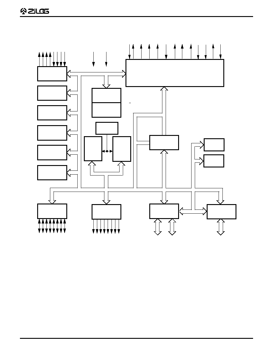
Z86193 Functional Block Diagram
Port 3
UART
32
˜
16
Divider
16 x 16
Multiplier
Port 2
I/O
(Bit Programmable)
ALU
FLAGS
Register
Pointers
Register
File
Page 0
256 x
8-Bit
Program
Counter
4
4
Port 0
Output
Input
Address or I/O
(Nibble Programmable)
8
Port 1
Low
Address/Data
Three 16-Bit
Counter/Timers
VCC GND
Interrupt
Control
Machine Timing, Emulation
and Instruction Control
/WR
/SYNC
XT
AL
ALE
/
RD
/RESET
SCLK
IACK
/W
AIT
/BREQ
/BACK
EV
AL
SEARCH
Machine
MERGE
Machine
Register
File
Page 1
208 x
8-Bit
Demultiplexed
Address
Low Address
3
Z86193
CPS DC-4206-01
P R E L I M I N A R Y
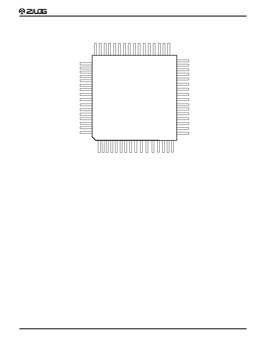
PIN CONFIGURATION
34
35
36
37
38
39
40
41
42
43
44
21
20
19
18
17
16
15
14
13
12
22
33
32
31
30
29
28
27
26
25
24
23
1 2 3 4 5 6 7 8
9 10 11
P21
N/C
/W
AIT
P24
P23
P22
GND
P20
P34//DM
A7
P17//AD7
N/C
N/C
/BACK
N/C
/RESET
/WR
/RD
ALE
P35
VCC
GND
IACK
P32
/SYNC
Z86193
VQFP
P00/A8
P01/A9
P02/A10
/BREQ
N/C
P14/AD4
A4
P13/AD3
A3
P12/AD2
A2
P11/AD1
A1
P10/AD0
A0
P07/A15
P06/A14
P05/A13
P04/A12
P03/A11
45
46
47
48
49
50
51
52
53
54
55
56
57
58
59
60
61
62
63
64
P25
P26
P27
P31
P36
GND
VCC
XTAL2
XTAL1
SCLK
P37
P30
/EVAL
N/C
P33
A6
P16/AD6
A5
P15/AD5
64-Pin VQFP Package
4
Z86193
CPS DC-4206-01
P R E L I M I N A R Y
Symbol Description
Min
Max
Units
V
CC
Supply Voltage*
≠0.3
+7.0
V
T
STG
Storage Temp
≠65
+150
C
T
A
Oper Ambient Temp
C
* Voltages on all pins with respect to GND.
See Ordering Information
Stress greater than those listed under Absolute Maximum
Ratings may cause permanent damage to the device. This
is a stress rating only; operation of the device at any
condition above those indicated in the operational sec-
tions of these specifications is not implied. Exposure to
absolute maximum rating conditions for an extended pe-
riod may affect device reliability.
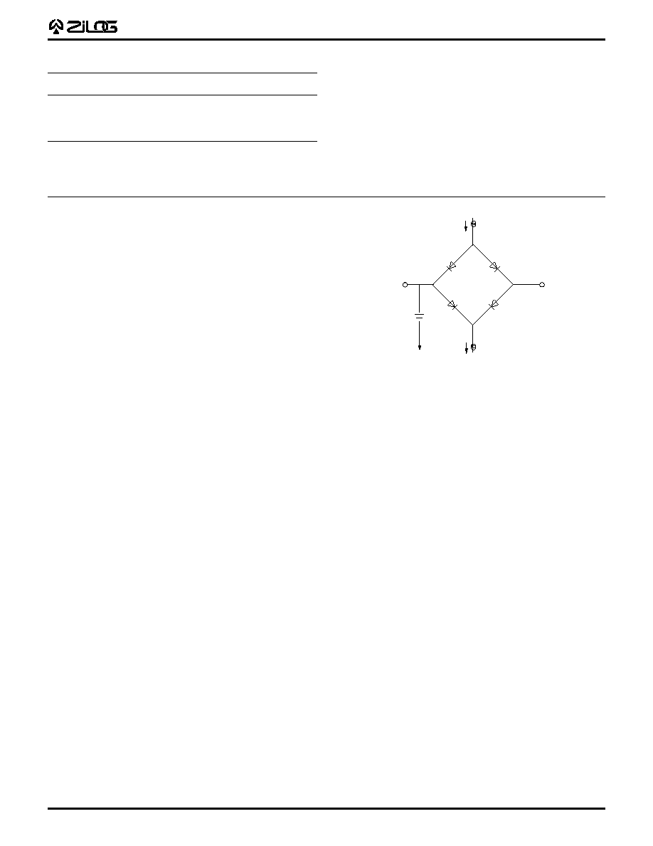
STANDARD TEST CONDITIONS
The characteristics listed below apply for standard test
conditions as noted. All voltages are referenced to GND.
Positive current flows into the referenced pin (Test Load
Diagram).
ABSOLUTE MAXIMUM RATINGS
V Commutation
DUT
Device Under Test
I
OH
OL
I
50 pf
Test Load Diagram
5
Z86193
CPS DC-4206-01
P R E L I M I N A R Y
DC ELECTRICAL CHARACTERISTICS
VCC = 5.0V
±
10%
T
A
= 0
∞
C to +70
∞
C
T y p i c a l
S y m
P a r a m e t e r
M i n
M a x
@ 25
∞
C
U n i t s
C o n d i t i o n s
Max Input Voltage
7
V
I
IN
250
µ
A
V
CH
Clock Input High Voltage
3.8
V
CC
V
Driven by External Clock Generator
V
CL
Clock Input Low Voltage
≠0.03
0.8
V
Driven by External Clock Generator
V
IH
Input High Voltage (P0,P1,P2) 2.0
V
CC
V
V
IH
Input High Voltage (P3)
2.2
V
CC
V
V
IL
Input Low Voltage
≠0.3
0.8
V
V
OH
Output High Voltge
2.4
V
I
OH
= ≠2.0 mA
V
OH
Output High Voltage
V
CC
≠100mV
V
I
OH
= ≠100
µ
A
V
OL
Output Low Voltage
0.4
V
I
OL
= + 4 mA
V
RH
Reset Input High Voltage
3.8
V
CC
V
V
Rl
Reset Input Low Voltage
≠0.03
0.8
V
I
IL
Input Leakage
≠2
2
µ
A
Test at 0V, V
CC
I
OL
Output Leakage
≠2
2
µ
A
Test at 0V, V
CC
I
IR
Reset Input Current
≠180
µ
A
V
RL
= 0V
I
CC
Supply Current
120
70
mA
@ 40 MHz [1]
I
CC1
Standby Current (HALT Mode)
30
20
mA
HALT Mode V
IN
= OV, V
CC
@ 40 MHz [1]
I
CC2
Standby Current
20
6
µ
A
STOP Mode V
IN
= OV, V
CC
[1]
I
AL
Auto Latch Current
≠16
16
5
µ
A
Note:
[1] All inputs driven to 0V, or V
cc
and outputs floating.
[2] Values are preliminary engineering estimates.
6
Z86193
CPS DC-4206-01
P R E L I M I N A R Y
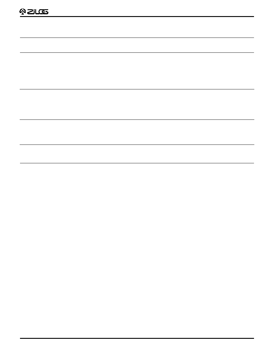
AC CHARACTERISTICS
External Memory Read/Write Timing Diagram
/DM
3
16
20
4
5
8
11
6
17
15
7
14
2
Port 0
Port 1
ALE
/RD
Port1
/WR
A0 - A7
D0 - D7 IN
D0 - D7 OUT
A0 - A7
21
19
10
A0 - A7
A0-A7
1
A8 - A15
9
External I/O or Memory Read/Write Timing Diagram

7
Z86193
CPS DC-4206-01
P R E L I M I N A R Y
AC CHARACTERISTICS
External I/O or Memory Read/Write Timing Table
No
Sym
Parameter
Max
Max
Units
1
TdA(ALE)
Address Valid To ALE Fall Delay
8
ns
2
ThALE(A)
ALE Fall To Address Hold Time
15
ns
3
TdALE(DI)
ALE Fall To Data In Req'd Valid Delay
75
ns
4
TwALE
ALE HIGH Width
10
ns
5
TdAZ(RD)
Address Float To /RD Fall
0
ns
6
TwRD
/RD Low Width
60
ns
7
TwWR
/WR Low Width
35
ns
8
TdRD(DI)
/RD Fall To Data in Req'd Valid Delay
40
ns
9
ThRD(DI)
/RD Rise to Data In Hold Time
0
ns
10
TdRDWR(A)
/RD or /WR Rise To Address Active Delay
20
ns
11
TdRDWR(ALE)
/RD or /WR Rise To ALE Delay
16
ns
14
TdDO(WR)
Data Out To /WR Fall Delay
12
ns
15
ThWR(DO)
/WR Rise To Data Out Hold Time
12
ns
16
TdA(DI)
Address Valid To Data In Req'd Valid Delay
90
ns
17
TdALE(RD)
ALE Fall To /RD Fall Delay
20
ns
19
TdDM(ALE)
/DM Valid To ALE Fall Delay
10
ns
20
TdRDWR(DM)
/RD or /WR Rise To /DM Valid Delay
15
ns
21
ThRDWR(A)
/RD or /WR Rise To Adress Valid Hold Time
15
ns
22
TdXT(SCR)
XTAL Falling To SCLK Rising
30
ns
23
TdXT(SCF)
XTAL Falling To SCLK Falling
30
ns
24
TdXT(RDF)
XTAL Falling To /RD Falling
40
ns
25
TdXT(RDR)
XTAL Falling To /RD Rising
30
ns
26
TdXT(WRF)
XTAL Falling To/WR Falling
40
ns
27
TdXT(WRR)
XTAL Falling To/WR Rising
30
ns
28
TsW(XT)
Wait Set Up Time
ns
29
ThW(XT)
Wait Hold Time
ns
30
TsW
Wait Width (One Wait Time)
ns
Notes:
1. Values based on external clock drive with a clock frequency.
2. Values are preliminary and are to be characterized.
3. When using extended memory timing, add 2TpC.
4. Timing numbers are given for minimum TpC.

8
Z86193
CPS DC-4206-01
P R E L I M I N A R Y
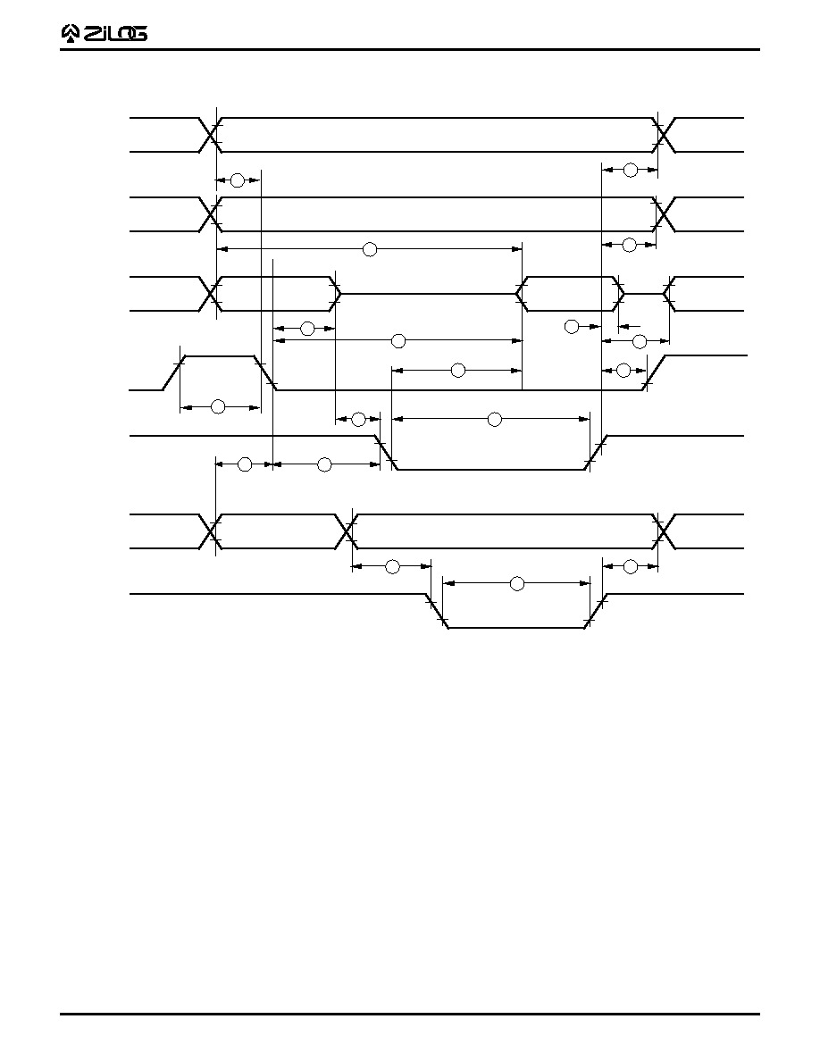
XTAL/SCLK To DSR and DSW Timing
XTAL1
SCLK
/RD
27
26
25
24
23
22
/WR
(External Clock Drive)
XTAL1
SCLK
ALE
/RD
WAIT
T1
T2
TW
TW
TW
T3
T1
32
30
31
XTAL/SCLK To WAIT Timing
9
Z86193
CPS DC-4206-01
P R E L I M I N A R Y
AC CHARACTERISTICS
Additional Timing Diagram
AC CHARACTERISTICS
Additional Timing Table
T
A
= 0
∞
C to +70
∞
C
40 MHz
No
Symbol Parameter
Min
Max
Units
Notes
1
TpC
Input Clock Period
25
1000
ns
[1]
2
TrC,TfC
Clock Imput Rise & Fall Times
4
ns
[1]
3
TwC
Input Clock Width
8
ns
[1]
4
TwTinL
Timer Input Low Width
75
ns
[2]
5
TwTinH
Timer Input High Width
3 TpC
ns
[2]
6
TpTin
Timer Input Period
8 TpC
ns
[2]
7
TrTin,TfTin Timer Input Rise & Fall Times
100
ns
[2]
8A
TwIL
Interrupt Request Input Low Times
70
ns
[2,4]
8B
TwIL
Interrupt Request Input Low Times
5 TpC
ns
[2,5]
9
TwIH
Interrupt Request Input High Times
3 TpC
ns
[2,3]
Notes:
[1] Clock timing references use 3.8V for a logic 1 and 0.8V for a logic 0.
[2] Timing references use 2.0V for a logic 1 and 0.8V for a logic 0.
[3] Interrupt references request through Port 3.
[4] Interrupt request through Port 3 (P33-P31)`.
[5] Interrupt request through Port 30.
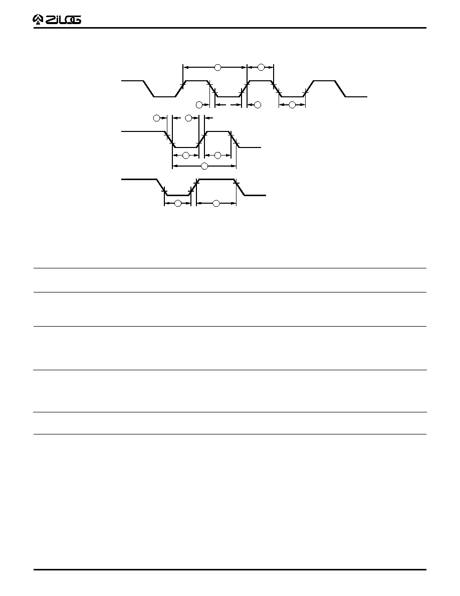
Additional Timing
Clock
1
3
4
8
2
2
3
T IN
IRQ N
6
5
7
7
9

10
Z86193
CPS DC-4206-01
P R E L I M I N A R Y
AC CHARACTERISTICS
Handshake Timing Diagrams
Input Handshake Timing
Data In
1
3
4
5
6
/DAV
(Input)
RDY
(Output)
Next Data In Valid
Delayed RDY
Delayed DAV
Data In Valid
2
Data Out
/DAV
(Output)
RDY
(Input)
Next Data Out Valid
Delayed RDY
Delayed DAV
Data Out Valid
7
8
9
10
11
Output Handshake Timing

11
Z86193
CPS DC-4206-01
P R E L I M I N A R Y
AC CHARACTERISTICS
Handshake Timing Table
T
A
= 0
∞
C to +70
∞
C
D a t a
N o
S y m b o l
P a r a m e t e r
M i n
M a x
U n i t s
D i r e c t i o n
1
TsDI(DAV)
Data In Setup Time to /DAV
0
ns
In
2
ThDI(DAV)
RDY to Data In Hold Time
0
ns
In
3
TwDAV
/DAV Width
80
ns
In
4
TdDAVIf(RDYf)
/DAV to RDY Delay
120
ns
In
5
TdDAVIr(RDYr)
DAV Rise to RDY Wait Time
40
ns
In
6
TdRDYOr(DAVIf)
RDY Rise to DAV Delay
0
ns
In
7
TdD0(DAV)
Data Out to DAV Delay
TpC
ns
Out
8
TdDAV0f(RDYIf)
/DAV to RDY Delay
0
ns
Out
9
TdRDYIf(DAVOr)
RDY to /DAV Rise Delay
120
ns
Out
10
TwRDY
RDY Width
80
ns
Out
11
TdRDYIr(DAVOf)
RDY Rise to DAV Wait Time
40
ns
Out
© 1995 by Zilog, Inc. All rights reserved. No part of this document
may be copied or reproduced in any form or by any means
without the prior written consent of Zilog, Inc. The information in
this document is subject to change without notice. Devices sold
by Zilog, Inc. are covered by warranty and patent indemnification
provisions appearing in Zilog, Inc. Terms and Conditions of Sale
only. Zilog, Inc. makes no warranty, express, statutory, implied or
by description, regarding the information set forth herein or
regarding the freedom of the described devices from intellectual
property infringement. Zilog, Inc. makes no warranty of mer-
chantability or fitness for any purpose. Zilog, Inc. shall not be
responsible for any errors that may appear in this document.
Zilog, Inc. makes no commitment to update or keep current the
information contained in this document.
Zilog's products are not authorized for use as critical compo-
nents in life support devices or systems unless a specific written
agreement pertaining to such intended use is executed between
the customer and Zilog prior to use. Life support devices or
systems are those which are intended for surgical implantation
into the body, or which sustains life whose failure to perform,
when properly used in accordance with instructions for use
provided in the labeling, can be reasonably expected to result in
significant injury to the user.
Zilog, Inc. 210 East Hacienda Ave.
Campbell, CA 95008-6600
Telephone (408) 370-8000
Telex 910-338-7621
FAX 408 370-8056
Low Margin:
Customer is advised that since this is a Preliminary CPS,
this product does not meet Zilog's internal guardbanded
test policies for the specification requested and is sup-
plied on an exception basis. Customer is cautioned that
delivery may be uncertain and that, in addition to all other
Pre-Characterization Product:
The product represented by this CPS is newly introduced
and Zilog has not completed the full characterization of the
product. The CPS states what Zilog knows about this
product at this time, but additional features or
non-conformance with some aspects of the CPS may be
found, either by Zilog or its customers in the course of
further application and characterization work. In addition,
Zilog cautions that delivery may be uncertain at times, due
to start-up yield issues.
limitations on Zilog liability stated on the front and back of
the acknowledgement, Zilog makes no claim as to quality
and reliability under the CPS. The product remains subject
to standard warranty for replacement due to defects in
materials and workmanship.