 | –≠–ª–µ–∫—Ç—Ä–æ–Ω–Ω—ã–π –∫–æ–º–ø–æ–Ω–µ–Ω—Ç: Z86230 | –°–∫–∞—á–∞—Ç—å:  PDF PDF  ZIP ZIP |

ZiLOG W
ORLDWIDE
H
EADQUARTERS
∑ 910 E. H
AMILTON
A
VENUE
∑ C
AMPBELL
, CA 95008
T
ELEPHONE
: 408.558.8500 ∑ F
AX
: 408.558.8300 ∑ I
NTERNET
:
HTTP
://
WWW
.Z
I
LOG.
COM
A
DVANCED
V
IOLENCE
B
LOCKING
AND
NTSC L
INE
21 XDS
P
RELIMINARY
P
RODUCT
S
PECIFICATION
PS000400-TVC0499
Z86230

2
Z86230--PRELIMINARY
PS000400-TVC0499
©1999 by ZiLOG, Inc. All rights reserved. Information in this publication concerning the devices, applica-
tions, or technology described is intended to suggest possible uses and may be superseded. ZiLOG, INC.
DOES NOT ASSUME LIABILITY FOR OR PROVIDE A REPRESENTATION OF ACCURACY OF
THE INFORMATION, DEVICES, OR TECHNOLOGY DESCRIBED IN THIS DOCUMENT. ZiLOG
ALSO DOES NOT ASSUME LIABILITY FOR INTELLECTUAL PROPERTY INFRINGEMENT
RELATED IN ANY MANNER TO USE OF INFORMATION, DEVICES, OR TECHNOLOGY
DESCRIBED HEREIN OR OTHERWISE. Except with the express written approval of ZiLOG, use of
information, devices, or technology as critical components of life support systems is not authorized. No
licenses are conveyed, implicitly or otherwise, by this document under any intellectual property rights.

PS000400-TVC0499
Z86230--PRELIMINARY
3
T
ABLE
OF
C
ONTENTS
1. A
RCHITECTURAL
O
VERVIEW
. . . . . . . . . . . . . . . . . . . . . . . . . . . . . . . . . . . . . . . . 9
1.1. B
LOCK
D
IAGRAM
AND
O
PERATIONAL
O
VERVIEW
. . . . . . . . . . . . . . . . . . . . 9
2. P
IN
D
ESCRIPTIONS
. . . . . . . . . . . . . . . . . . . . . . . . . . . . . . . . . . . . . . . . . . . . . . 13
3. Z86230 F
EATURE
S
ET
. . . . . . . . . . . . . . . . . . . . . . . . . . . . . . . . . . . . . . . . . . . 16
3.1. VBI D
ATA
P
ROCESSING
. . . . . . . . . . . . . . . . . . . . . . . . . . . . . . . . . . . . . 16
3.2. S
ERIAL
C
OMMUNICATIONS
I
NTERFACE
. . . . . . . . . . . . . . . . . . . . . . . . . . 16
3.3. S
ETUP
AND
O
PERATIONAL
C
ONTROL
. . . . . . . . . . . . . . . . . . . . . . . . . . . 17
4. S
ERIAL
C
OMMUNICATIONS
I
NTERFACE
. . . . . . . . . . . . . . . . . . . . . . . . . . . . . . . 18
4.1. I
2
C B
US
O
PERATION
. . . . . . . . . . . . . . . . . . . . . . . . . . . . . . . . . . . . . . . 18
5. C
OMMANDS
. . . . . . . . . . . . . . . . . . . . . . . . . . . . . . . . . . . . . . . . . . . . . . . . . . 23
5.1. S
ERIAL
P
ORT
C
OMMANDS
. . . . . . . . . . . . . . . . . . . . . . . . . . . . . . . . . . . 23
5.2. READ
AND
WRITE C
OMMANDS
. . . . . . . . . . . . . . . . . . . . . . . . . . . . . . 23
5.3. W
RITING
TO
THE
Z86230 . . . . . . . . . . . . . . . . . . . . . . . . . . . . . . . . . . . . 24
6. C
ONTROL
R
EGISTERS
. . . . . . . . . . . . . . . . . . . . . . . . . . . . . . . . . . . . . . . . . . . . 25
6.1. R
EGISTERS
S
UMMARY
. . . . . . . . . . . . . . . . . . . . . . . . . . . . . . . . . . . . . . 25
6.2. XDS D
ATA
R
ECOVERY
. . . . . . . . . . . . . . . . . . . . . . . . . . . . . . . . . . . . . . 35
6.3. Z86230 C
OMMANDS
AND
R
EGISTERS
S
UMMARY
. . . . . . . . . . . . . . . . . . 38
6.4. P
ROGRAM
B
LOCKING
M
AP
. . . . . . . . . . . . . . . . . . . . . . . . . . . . . . . . . . . 39
7. D
EMONSTRATION
P
ROGRAMS
. . . . . . . . . . . . . . . . . . . . . . . . . . . . . . . . . . . . . 42
7.1. C
OMMUNICATING
WITH
THE
Z86230 . . . . . . . . . . . . . . . . . . . . . . . . . . . 42
7.2. I
2
C O
PERATION
. . . . . . . . . . . . . . . . . . . . . . . . . . . . . . . . . . . . . . . . . . . 42
7.3. IICO P
ROGRAM
. . . . . . . . . . . . . . . . . . . . . . . . . . . . . . . . . . . . . . . . . . . 42
7.4. G
ENERAL
C
OMMANDS
. . . . . . . . . . . . . . . . . . . . . . . . . . . . . . . . . . . . . . 43
7.5. SCRIPTI P
ROGRAM
. . . . . . . . . . . . . . . . . . . . . . . . . . . . . . . . . . . . . . . . 43
7.6. S
CRIPT
F
ILES
. . . . . . . . . . . . . . . . . . . . . . . . . . . . . . . . . . . . . . . . . . . . . 43
8. E
LECTRICAL
C
HARACTERISTICS
. . . . . . . . . . . . . . . . . . . . . . . . . . . . . . . . . . . . . 46
8.1. A
BSOLUTE
M
AXIMUM
R
ATINGS
1 . . . . . . . . . . . . . . . . . . . . . . . . . . . . . . 46
8.2. S
TANDARD
T
EST
C
ONDITIONS
. . . . . . . . . . . . . . . . . . . . . . . . . . . . . . . . 46
8.3. DC C
HARACTERISTICS
. . . . . . . . . . . . . . . . . . . . . . . . . . . . . . . . . . . . . . 47
8.4. AC
AND
T
IMING
C
HARACTERISTICS
. . . . . . . . . . . . . . . . . . . . . . . . . . . . . 47
8.5. E
LECTRICAL
C
HARACTERISTICS
. . . . . . . . . . . . . . . . . . . . . . . . . . . . . . . . 47
9. A
PPLICATION
I
NFORMATION
. . . . . . . . . . . . . . . . . . . . . . . . . . . . . . . . . . . . . . . 50
9.1. R
EFERENCE
D
ESIGNS
. . . . . . . . . . . . . . . . . . . . . . . . . . . . . . . . . . . . . . . 50
10. P
ACKAGING
. . . . . . . . . . . . . . . . . . . . . . . . . . . . . . . . . . . . . . . . . . . . . . . . . . 53
11. O
RDERING
I
NFORMATION
. . . . . . . . . . . . . . . . . . . . . . . . . . . . . . . . . . . . . . . . 54
11.1. P
ART
N
UMBER
D
ESCRIPTION
. . . . . . . . . . . . . . . . . . . . . . . . . . . . . . . . 54
12. P
RECHARACTERIZATION
P
RODUCT
. . . . . . . . . . . . . . . . . . . . . . . . . . . . . . . . . 55
C
USTOMER
F
EEDBACK
F
ORM
. . . . . . . . . . . . . . . . . . . . . . . . . . . . . . . . . . . . 56
Z86230 P
RODUCT
S
PECIFICATION
. . . . . . . . . . . . . . . . . . . . . . . . . . . . 56
C
USTOMER
I
NFORMATION
. . . . . . . . . . . . . . . . . . . . . . . . . . . . . . . . . . 56
P
RODUCT
I
NFORMATION
. . . . . . . . . . . . . . . . . . . . . . . . . . . . . . . . . . . 56
R
ETURN
I
NFORMATION
. . . . . . . . . . . . . . . . . . . . . . . . . . . . . . . . . . . . 56
P
ROBLEM
D
ESCRIPTION
OR
S
UGGESTION
. . . . . . . . . . . . . . . . . . . . . . . 56

4
Z86230--PRELIMINARY
PS000400-TVC0499

PS000400-TVC0499
Z86230--PRELIMINARY
5
L
IST
OF
F
IGURES
F
IGURE
1.
V
OLTAGE
/C
IRCUIT
R
EFERENCE
. . . . . . . . . . . . . . . . . . . . . . . . . . . . . . 11
F
IGURE
2.
F
UNCTIONAL
B
LOCK
D
IAGRAM
. . . . . . . . . . . . . . . . . . . . . . . . . . . . . . 12
F
IGURE
3.
18-P
IN
DIP
AND
SOIC D
EVICES
. . . . . . . . . . . . . . . . . . . . . . . . . . . . 13
F
IGURE
4.
I
2
C B
US
WRITE (C
OMMAND
) . . . . . . . . . . . . . . . . . . . . . . . . . . . . . . 20
F
IGURE
5.
I
2
C B
US
READ (C
OMMAND
) . . . . . . . . . . . . . . . . . . . . . . . . . . . . . . . 21
F
IGURE
6.
I
2
C S
ERIAL
T
IMING
. . . . . . . . . . . . . . . . . . . . . . . . . . . . . . . . . . . . . . 22
F
IGURE
7.
S
TANDARD
T
EST
L
OAD
. . . . . . . . . . . . . . . . . . . . . . . . . . . . . . . . . . . 46
F
IGURE
8.
Z86230 R
EFERENCE
C
IRCUIT
. . . . . . . . . . . . . . . . . . . . . . . . . . . . . . . 50
F
IGURE
9.
PCB D
ESIGN
OF
Z86230 R
EFERENCE
C
IRCUIT
. . . . . . . . . . . . . . . . . . 52
F
IGURE
10. 18-L
EAD
DIP P
ACKAGE
D
IAGRAM
. . . . . . . . . . . . . . . . . . . . . . . . . . . 53
F
IGURE
11. 18-L
EAD
SOIC P
ACKAGE
D
IAGRAM
. . . . . . . . . . . . . . . . . . . . . . . . . . 53

6
Z86230--PRELIMINARY
PS000400-TVC0499

PS000400-TVC0499
Z86230--PRELIMINARY
7
L
IST
OF
T
ABLES
T
ABLE
1.
P
IN
D
ESCRIPTIONS
. . . . . . . . . . . . . . . . . . . . . . . . . . . . . . . . . . . . . . 13
T
ABLE
2.
Z86230 S
ERIAL
C
ONTROL
S
IGNALS
. . . . . . . . . . . . . . . . . . . . . . . . . . 16
T
ABLE
3.
U
SER
P
ROGRAMMABLE
F
EATURES
. . . . . . . . . . . . . . . . . . . . . . . . . . . 17
T
ABLE
4.
Z86230 I
2
C S
LAVE
A
DDRESSES
. . . . . . . . . . . . . . . . . . . . . . . . . . . . 18
T
ABLE
5.
Z86230 I
2
C READ B
ANK
S
ELECT
(RBS) C
OMMAND
. . . . . . . . . . . . 20
T
ABLE
6.
I
2
C S
ERIAL
T
IMING
M
IN
/M
AX
. . . . . . . . . . . . . . . . . . . . . . . . . . . . . . 22
T
ABLE
7.
B
ASIC
S
ERIAL
C
OMMANDS
. . . . . . . . . . . . . . . . . . . . . . . . . . . . . . . . 23
T
ABLE
8.
RDS1≠READ O
NE
B
YTE
. . . . . . . . . . . . . . . . . . . . . . . . . . . . . . . . . . 24
T
ABLE
9.
RSD2≠R
EAD
T
WO
B
YTES
. . . . . . . . . . . . . . . . . . . . . . . . . . . . . . . . . 24
T
ABLE
10.
WR
XX
≠W
RITE
R
EGISTER
XX
. . . . . . . . . . . . . . . . . . . . . . . . . . . . . . . 24
T
ABLE
11.
S
ERIAL
S
TATUS
R
EGISTER
. . . . . . . . . . . . . . . . . . . . . . . . . . . . . . . . . 25
T
ABLE
12.
C
ONFIGURATION
R
EGISTER
. . . . . . . . . . . . . . . . . . . . . . . . . . . . . . . . 25
T
ABLE
13.
XDS D
ATA
A
CTIVITY
R
EGISTER
. . . . . . . . . . . . . . . . . . . . . . . . . . . . . 26
T
ABLE
14.
XDS F
ILTER
R
EGISTER
. . . . . . . . . . . . . . . . . . . . . . . . . . . . . . . . . . . 26
T
ABLE
15.
XDS S
ECONDARY
F
ILTER
S
ETTINGS
. . . . . . . . . . . . . . . . . . . . . . . . . 27
T
ABLE
16.
I
NTERRUPT
R
EQUEST
R
EGISTER
. . . . . . . . . . . . . . . . . . . . . . . . . . . . 27
T
ABLE
17.
I
NTERRUPT
M
ASK
R
EGISTER
. . . . . . . . . . . . . . . . . . . . . . . . . . . . . . . 28
T
ABLE
18.
C
ONTENT
A
DVISORY
R
ATINGS
S
ELECT
R
EGISTER
1 . . . . . . . . . . . . . . 28
T
ABLE
19.
C
ONTENT
A
DVISORY
R
ATINGS
S
ELECT
R
EGISTER
2 . . . . . . . . . . . . . . 29
T
ABLE
20.
C
ONTENT
A
DVISORY
R
ATINGS
S
ELECT
R
EGISTER
3 . . . . . . . . . . . . . . 30
T
ABLE
21.
C
ONTENT
A
DVISORY
R
ATINGS
S
ELECT
R
EGISTER
4 . . . . . . . . . . . . . . 31
T
ABLE
22.
C
ONTENT
A
DVISORY
R
EGISTER
1 . . . . . . . . . . . . . . . . . . . . . . . . . . . . 31
T
ABLE
23.
C
ONTENT
A
DVISORY
R
EGISTER
2 . . . . . . . . . . . . . . . . . . . . . . . . . . . . 32
T
ABLE
24.
B
LOCKING
C
ONTROL
R
EGISTER
1 . . . . . . . . . . . . . . . . . . . . . . . . . . . . 32
T
ABLE
25.
C
ONTENT
A
DVISORY
R
ATINGS
S
ELECT
R
EGISTER
5 . . . . . . . . . . . . . . 32
T
ABLE
26.
C
ONTENT
A
DVISORY
R
ATINGS
S
ELECT
R
EGISTER
6 . . . . . . . . . . . . . . 34
T
ABLE
27.
B
LOCKING
C
ONTROL
R
EGISTER
2 . . . . . . . . . . . . . . . . . . . . . . . . . . . . 34
T
ABLE
28.
XDS D
ATA
E
XTRACTION
E
XAMPLE
F
ILTER
S
ETTINGS
. . . . . . . . . . . . . 36
T
ABLE
29.
Z86230 S
UMMARY
OF
C
ONTROL
C
OMMANDS
. . . . . . . . . . . . . . . . . . 38
T
ABLE
30.
S
UMMARY
OF
Z86230 I
NTERNAL
R
EGISTERS
. . . . . . . . . . . . . . . . . . 39
T
ABLE
31.
MPAA M
ATRIX
(U
SE
C
ONTENT
A
DVISORY
R
ATING
R
EGISTER
. . . . . . 40
T
ABLE
32.
TV P
ARENTAL
G
UIDELINES
M
ATRIX
. . . . . . . . . . . . . . . . . . . . . . . . . 40
T
ABLE
33.
C
ANADIAN
E
NGLISH
M
ATRIX
. . . . . . . . . . . . . . . . . . . . . . . . . . . . . . 41
T
ABLE
34.
C
ANADIAN
F
RENCH
M
ATRIX
. . . . . . . . . . . . . . . . . . . . . . . . . . . . . . . 41
T
ABLE
35.
C
ONFIGURATION
R
EGISTER
S
CRIPT
F
ILES
. . . . . . . . . . . . . . . . . . . . . . 44
T
ABLE
36.
DC C
HARACTERISTICS
. . . . . . . . . . . . . . . . . . . . . . . . . . . . . . . . . . . 47
T
ABLE
37.
C
OMPOSITE
V
IDEO
I
NPUT
. . . . . . . . . . . . . . . . . . . . . . . . . . . . . . . . . 47
T
ABLE
38.
N
ON
-S
TANDARD
V
IDEO
S
IGNALS
. . . . . . . . . . . . . . . . . . . . . . . . . . . . 47

8
Z86230--PRELIMINARY
PS000400-TVC0499
T
ABLE
39.
HIN/XIN S
IGNAL
I
NPUT
. . . . . . . . . . . . . . . . . . . . . . . . . . . . . . . . . . 48
T
ABLE
40.
L
INE
21 I
NPUT
P
ARAMETERS
. . . . . . . . . . . . . . . . . . . . . . . . . . . . . . . 49
T
ABLE
41.
R
ECOMMENDED
C
OMPONENT
V
ALUES
--R
EFERENCE
C
IRCUIT
. . . . . . . 51

B
LOCK
D
IAGRAM
AND
O
PERATIONAL
O
VERVIEW
A
RCHITECTURAL
O
VERVIEW
PS000400-TVC0499
Z86230--PRELIMINARY
9
1. ARCHITECTURAL
OVERVIEW
The Z86230 is a stand-alone integrated circuit, capable of processing Extended
Data Services (XDS) in Field 2 of the Vertical Blanking Interval (VBI) of a video
frame. This device conforms to the transmission format defined in the Television
Decoder Circuits Act of 1990, in accordance with the Electronics Industry Associ-
ation specification EIA-608A and EIA-744A.
The XDS data is processed to provide either a Program Blocking signal (PB) or a
recovered XDS data packet. The PB matches the contents of the recovered Con-
tent Advisory packet to the user selections input on the decoder. On-chip XDS fil-
ters in the Z86230 are fully-programmable, enabling recovery of only those XDS
data packets selected for use in TVs, VCRs, and Set-Top boxes.
In addition, the Z86230 is ideally suited to monitor Picture-In-Picture (PiP) win-
dow video for violence blocking and other XDS data services.
Highlights of the Z86230 include:
1. A stand-alone Line 21 Decoder for Extended Data Services (XDS).
2. Extractable XDS data from the input video.
3. Full output of a selectable V-Chip Program Blocking signal (PB).
4. Selectable XDS filter parameters from a list of preprogrammed values.
5. Minimal communications and control overhead that provides simple
implementation of Violence Blocking and Auto Clock Set Features.
6. Full output of the recovered XDS data through the I
2
C serial communication
port.
7. Two different slave addresses that are selectable in the I
2
C serial
communication port.
8. Selectable
NTSC
or
PAL
operation.
1.1 B
LOCK
D
IAGRAM
AND
O
PERATIONAL
O
VERVIEW
The Z86230 is designed to process XDS data of the television VBI. The device
requires both a Composite Video and a horizontal timing signal (
HIN/XIN
input).
Several passive components are required for proper operation. Commands are
input to enable the decoder to process and control the V-Chip response to the XDS
Content Advisory packet. The Z86230 can also be configured to operate with
PAL
video signals. In
PAL
mode, the device decodes information encoded into VBI
Line 22. The encoded data must conform to the waveform and command structure
defined for
NTSC
Line 21 operation.
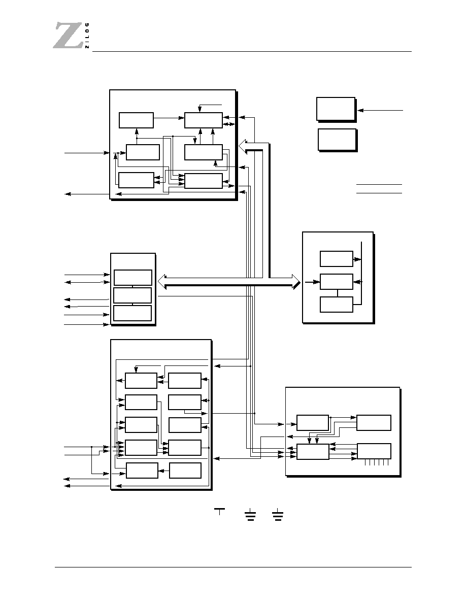
Figure 1 illustrates the Functional Block Diagram of the Z86230.
A
RCHITECTURAL
O
VERVIEW
B
LOCK
D
IAGRAM
AND
O
PERATIONAL
O
VERVIEW
10
Z86230--PRELIMINARY
PS000400-TVC0499
F
IGURE
1. F
UNCTIONAL
B
LOCK
D
IAGRAM
Command
Processor
Address
Decoder
RAM
Buffer
VW
Data Slicer
Data CLK
Recovery
Sliced
Data
Dual Clamp
Lock
STG
SYNC Slicer
PG
H Lock
FEW
AW
Status Reg
Test Reg
Slice Level
CG Logic
PH1
PH2
FR & MUX
I Dr & MUX
OSC
O/S
Control
CG Lines
MSYNC
COMP SYNC
POR Ckt
V/I Ref
Addr Bus
Serial
Control Port
MSYNC
Data Bus
PB
I
2
C SEL
NRST
SCLK
SDA
VIDEO
CSYNC
RREF
HIN/XIN
LPF
V
DD
V
SS
V
SS
(A)
DCLK
Data Line
DCLK
DIV
C CIR
V Lock
Line & Field
FLD
LS
SFLD
SLS
Control
CCLK
CW
Line & Fld Dec
MSGR
CLK DIV
COMP
H SEL
X
OUT
NC
INTRO
NC

B
LOCK
D
IAGRAM
AND
O
PERATIONAL
O
VERVIEW
A
RCHITECTURAL
O
VERVIEW
PS000400-TVC0499
Z86230--PRELIMINARY
11
1.1.1 Input Signals
The Composite Video input should be a signal which is nominally 1.0 Volt p-p,
with sync tips negative and band limited to 600 kHz. The Z86230 operates with an
input level variation of ±3 dB.
The
HIN/XIN
input signal is required to bring the voltage-controlled oscillator
(VCO) close to the required operating frequency.
1.1.2 Video Input Signal Processing
The Composite Video input is AC-coupled to the device where the sync tip is
internally clamped to a fixed reference voltage.
The Data Slicer extracts a clean CMOS-level data signal by slicing the signal at its
midpoint. The slice level is established on an adaptive basis during Line 21.
The Sync Slicer processes the clamped Composite Video signal to extract Com-
posite Sync. This signal is used to lock the internal logic to the incoming video.
The slice level is stored on the sync slice capacitor,
CSYNC
.
The Data Clock Recovery circuit operates in conjunction with the
Horizontal (H)
Lock
circuit. These circuits produce a data clock (
DCLK
) and, when Line 21 code
appears,
DCLK
phase lock is achieved during the clock run-in burst (used to
reclock the sliced data). When phase lock is established,
DCLK
is maintained until
a change in the video signal occurs.
1.1.3 Voltage-Controlled Oscillator (VCO) and One-Shot
All internal timing and synchronizing signals are derived from the on-board 12-
MHz VCO. Its output is the
DCLK
signal used to drive the Horizontal and Vertical
counter chains.
The One-Shot circuit produces a horizontal timing signal derived from the incom-
ing video.
The VCO exhibits stable gain characteristics and good power supply rejection.
1.1.4 Timing and Counting Circuits
The
DCLK
is divided to generate the horizontal timing signals
H
and
2H
.The
H
signal is further divided in the line counter (
LINE CNTR
)
and field counter (
FLD
CNTR
) to produce the various decodes used to establish vertical lock and to time
the control functions required for proper operation.
1.1.5 Command Processor
The Command Processor controls the manipulation of the data for storage. During
the recovery time, the command processor, in conjunction with the data recovery
circuits, recovers the XDS data.
A
RCHITECTURAL
O
VERVIEW
B
LOCK
D
IAGRAM
AND
O
PERATIONAL
O
VERVIEW
12
Z86230--PRELIMINARY
PS000400-TVC0499
1.1.6 Decoder Control Circuit
The Decoder Control circuit block is the users communications port. This circuit
converts the information from the control port into the internal control signals
required to establish the operating mode of the decoder.
The Z86230 responds to its slave address for both the
READ
and
WRITE
condi-
tions. If the
READ
bit is Low (indicating a
WRITE
sequence), then the Z86230
responds with an Acknowledge. The master should then send an address byte fol-
lowed by a data byte. If the
READ
bit is High (indicating a
READ
sequence), then
the Z86230 responds with an Acknowledge followed sequentially by a status byte
and a data byte.
READ
data is only available through indirect addressing.
WRITE
addressing exhibits both indirect and direct modes. The busy bit in the status byte
indicates if the
WRITE
operation is completed or if
READ
data is available.
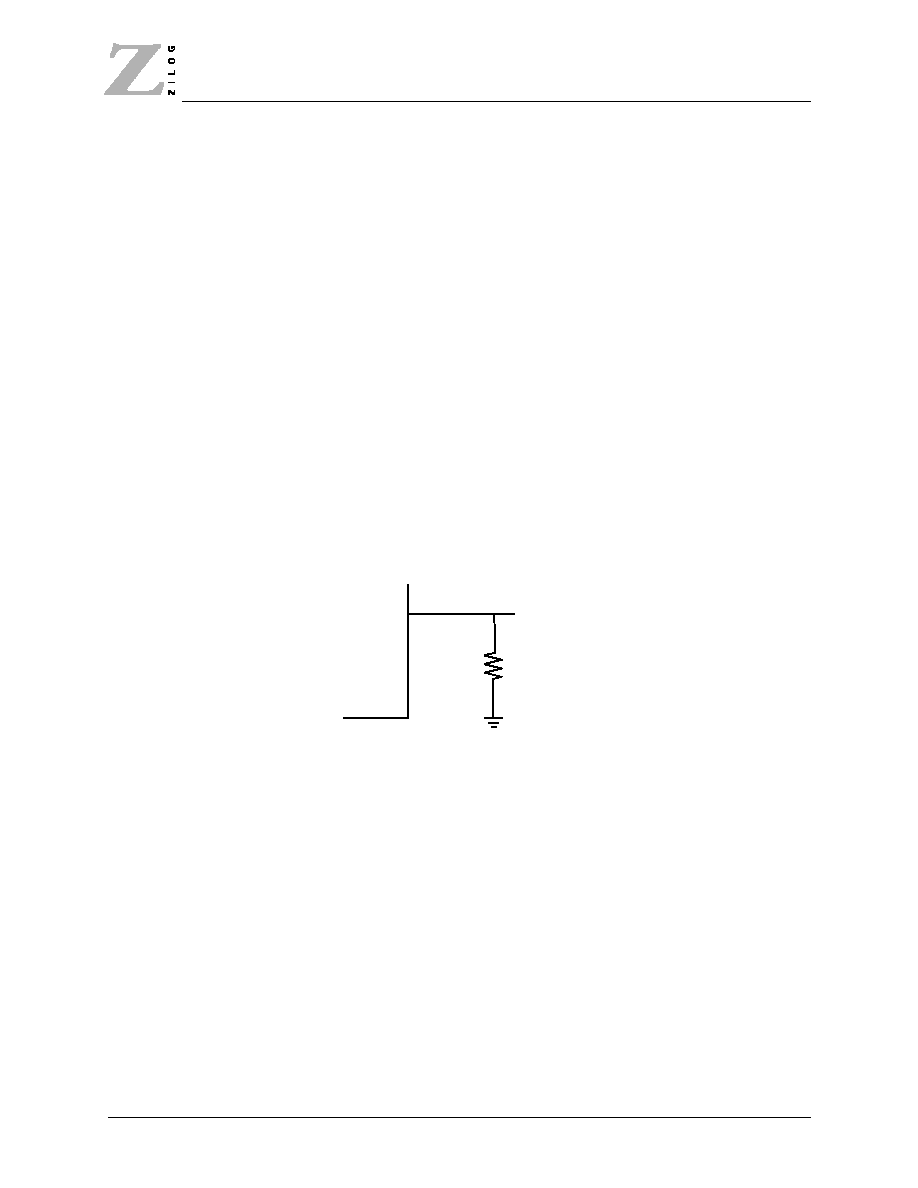
1.1.7 Voltage/Current Reference
The Voltage/Current reference circuit uses an externally connected resistor to
establish the reference levels that are used throughout the Z86230. For a minimal
investment, the use of an external resistor can also provide improved internal pre-
cision.
F
IGURE
2. V
OLTAGE
/C
IRCUIT
R
EFERENCE
RREF
10 k
±2%
Pin 10
GND
B
LOCK
D
IAGRAM
AND
O
PERATIONAL
O
VERVIEW
P
IN
D
ESCRIPTIONS
PS000400-TVC0499
Z86230--PRELIMINARY
13
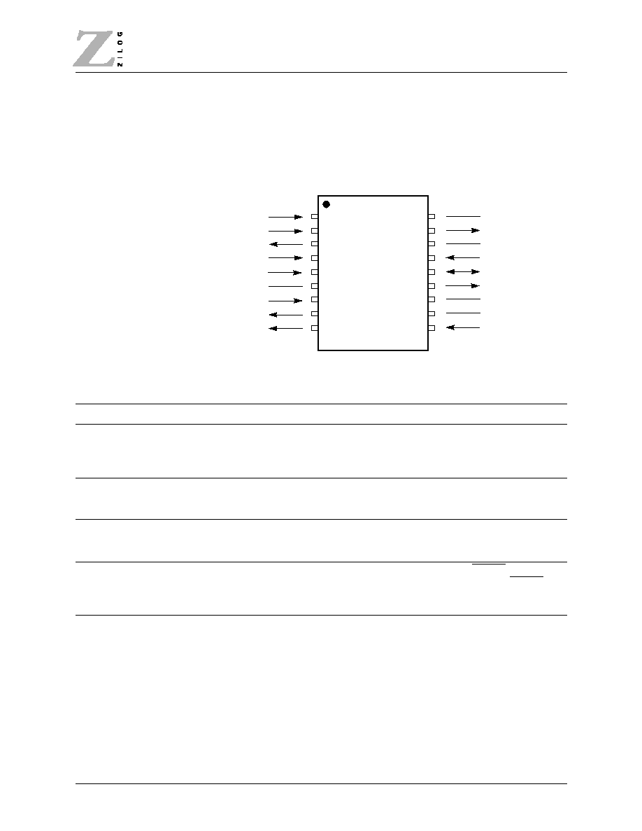
2. PIN
DESCRIPTIONS
There are 2 different packages, 18-pin DIP and 18-pin SOIC, available in the
Z86230.
F
IGURE
3. 18-P
IN
DIP
AND
SOIC D
EVICES
T
ABLE
1. P
IN
D
ESCRIPTIONS
Symbol
Pin #
Function
Direction
Description
I
2
C SEL
1
I
2
C Address Select
Input
Selects I
2
C Address. Low(0) sets the slave
address to
28h
for WRITE and
29h
for
READ. HIGH(1) sets the slave address to
2Ah
for WRITE and
2Bh
for READ.
H SEL
2
HIN/XIN Select
Input
Selects the source of the horizontal frequency
signal. Tying pin 2 HIGH(1) selects XIN mode.
Tying pin 2 Low(0) selects HIN mode.
X
OUT
3
XTAL Output
Output
When operating in XIN mode this pin is the
output pin for the XTAL circuit. In HIN mode,
the X
OUT
pin is a no connect (NC).
NRST
4
RESET
Input
Capable of being tied to an RESET signal if a
Power-On Reset action is required. RESET
must be held Low(0) for at least 100ns;
otherwise, the pin must be tied HIGH(1).
1
2
3
4
5
6
7
8
9
17
16
15
14
13
12
11
10
18
I
2
C SEL
H SEL
X
OUT
NRST
HIN/XIN
V
SS
VIDEO
CSYNC
LPF
NC
INTRO
NC
SCLK
SDA
PB
V
DD
V
SS
(A)
RREF
Z86230
DIP/SOIC
P
IN
D
ESCRIPTIONS
B
LOCK
D
IAGRAM
AND
O
PERATIONAL
O
VERVIEW
14
Z86230--PRELIMINARY
PS000400-TVC0499
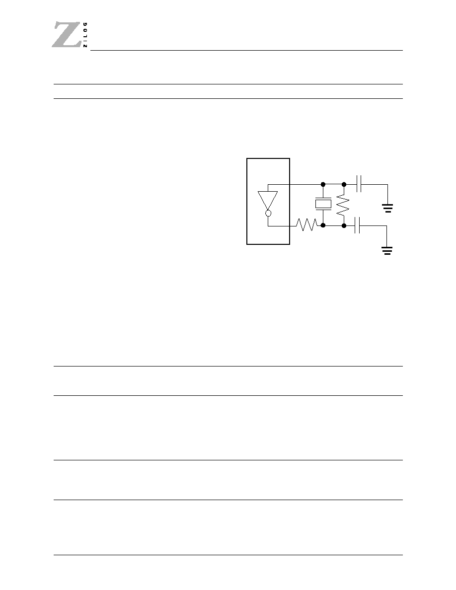
HIN/XIN
5
Horizontal In/XTAL In Input
When XTAL mode is selected, the horizontal
frequency signal may be generated on the chip
using the external 32.768-kHz crystal circuit, as
shown below. This circuit must be connected
between pin 5 and 3.
When HIN mode is selected, a horizontal
frequency signal must be supplied to the pin.
This signal must be within +3% Fh; however,
the frequency signal can exhibit any polarity
and duty cycle. Alternatively, an external
horizontal frequency signal may be used in
XIN mode operation. In this case, the signal
must exhibit a frequency of 32.768 KHz.
V
SS
6
Power Supply
(digital) GND
N/A
This pin is the lowest potential power pin for
the digital circuit that is typically tied to
system ground.
VIDEO
7
Composite Video
Input
Composite NTSC video input, 1.0V p-p (nom),
band limited to 600 kHz. The circuit operates
with signal variation between 0.7≠1.4V p-p.
The polarity is sync tips negative. This signal
pin should be AC-coupled through a 0.1 µF
capacitor and driven by a source impedance
of 470 ohms or less.
CSYNC
8
Composite Sync
Output
Sync slice level. A 0.1 µmF capacitor must be
tied between this pin and analog ground
V
SS
(A). This capacitor stores the sync slice
level voltage.
T
ABLE
1. P
IN
D
ESCRIPTIONS
Symbol
Pin #
Function
Direction
Description
Z86230
Y1
32.768KHz
R1
22M
R2
470K
C1
10pF
C2
20pF
Pin 5
Pin 3
Crystal Type: 32.768 kHz, CL=12.5pF
Series Resistance < 35 kOhms
Epson, C-001R 32.768 kHz or
Fox, NC26, NC28 or equivalent
(18 kOhms typ)

B
LOCK
D
IAGRAM
AND
O
PERATIONAL
O
VERVIEW
P
IN
D
ESCRIPTIONS
PS000400-TVC0499
Z86230--PRELIMINARY
15
LPF
9
Loop Filter
Output
Loop Filter. A series RC low-pass filter must be
tied between this pin and analog ground
V
SS
(A). There must also be second capacitor
from the pin to V
SS
(A).
RREF
10
Resistor Reference
Input
Reference setting resistor. This resistor must
be 10 kOhms, ±2%.
V
SS
(A)
11
Power Supply
(Anlalog) GND
N/A
This pin is the lowest potential power pin for
the analog circuit that is typically tied to
system ground.
V
DD
12
Power Supply +5V
N/A
The voltage on this pin is nominally 5.0 Volts,
and may range between 4.75 to 5.25 Volts with
respect to the V
SS
pins.
PB
13
Program Blocking
Output
This pin is HIGH(1) when the received Content
Advisory packet matches the viewers
selection as entered into the Content Advisory
Rating Select registers.
SDA
14
Serial Data
In/Output
This pin is the bidirectional data line for
sending and receiving serial data.
SCLK
15
Serial Clock
Input
This pin acts as an input pin for the serial clock
signal from the I
2
C master. The clock rate is
expected to be within I
2
C limits.
NC
16
No Connect
N/A
No Connect
INTRO
17
Interrupt Output
Output
This pin provides an interrupt signal to the
master control device in accordance with the
settings in the Interrupt Mask Register.
NC
18
No Connect
N/A
No Connect
T
ABLE
1. P
IN
D
ESCRIPTIONS
Symbol
Pin #
Function
Direction
Description
LPF
CSYNC
C6
C5
C7
R5
8
9

Z86230 F
EATURE
S
ET
VBI D
ATA
P
ROCESSING
16
Z86230--PRELIMINARY
PS000400-TVC0499
3.
Z86230 FEATURE SET
The primary features of the Z86230 are briefly described below. More complete
descriptions can be found in later sections of this document.
3.1 VBI
D
ATA
P
ROCESSING
The Z86230 extracts the XDS data in Line 21 of the incoming video. Processing
includes:
1.
Extracting XDS data from the input video.
2. Outputting the V-Chip Program Blocking signal (PB).
3. Outputting the XDS data through the serial port (raw or filtered).
4. Selecting the XDS filter parameters from a list of preprogrammed values.
5. Selecting either
NTSC
or
PAL
operation.
3.2 S
ERIAL
C
OMMUNICATIONS
I
NTERFACE
Communications and control of the Z86230 is possible through the I
2
C serial con-
trol interface, composed of:
1.
A 2-wire I
2
C interface.
2. Two available slave addresses.
T
ABLE
2. Z86230 S
ERIAL
C
ONTROL
S
IGNALS
Signal
I
2
C SEL
SCLK
SDA
Pin #
1
15
14
I/O
I
I
I/O
1
st
I
2
C Address (
28h
(W)/
29h
(R))
0
CLK
Data
2
nd
I
2
C Address(
2Ah
(W)/
2Bh
(R))
1
CLK
Data

S
ETUP
AND
O
PERATIONAL
C
ONTROL
Z86230 F
EATURE
S
ET
PS000400-TVC0499
Z86230--PRELIMINARY
17
3.3 S
ETUP
AND
O
PERATIONAL
C
ONTROL
The Z86230 is fully programmable through its flexible I
2
C serial communication
port. The following tables provide a partial list of User-Programmable Features
and Default Conditions upon
RESET
.
T
ABLE
3. U
SER
P
ROGRAMMABLE
F
EATURES
Feature
Parameters
RESET Condition
Video Standard
NTSC/PAL
NTSC
VCO Lock
Video/External HIN
Video
H Lock
Video/External HIN
Video
XDS Data Output
Raw/Filtered
OFF
Contents Advisory Rating
Select
ON/OFF
OFF
Program Blocking
ON/OFF
ON
Blocking
No Rating
Programs
ON/OFF
OFF
Program Unblock Hold Off Up to 254 Vertical Frames
0

S
ERIAL
C
OMMUNICATIONS
I
NTERFACE
I
2
C B
US
O
PERATION
18
Z86230--PRELIMINARY
PS000400-TVC0499
4.
SERIAL COMMUNICATIONS INTERFACE
Commands and data are sent to and from the Z86230 through its I
2
C serial com-
munications interface. This port is the path for setting the configuration and oper-
ational modes of the device. The interface is also used as the port for outputting
the recovered XDS data.
4.1 I
2
C B
US
O
PERATION
The Z86230 supports a bidirectional 2-wire bus and data transmission protocol.
The bus is controlled by the master device, which generates the serial clock
(
SCLK
), controls the bus access, and generates the
START
and
STOP
conditions.
The serial data (
SDA
) pin is the bidirectional data line. The Z86230 is a slave
device with two possible slave addresses. When the
I
2
C SEL
pin is Low, the slave
address is
28h
for
WRITE
and
29h
for
READ
. When the
I
2
C
SEL
pin is High,
the slave address is
2Ah
for
WRITE
and
2Bh
for
READ
.
The Z86230 can receive or transmit data under control of the master device. Com-
munication is initiated when the master device sends the
START
condition fol-
lowed by the Z86230 Slave Address
READ
byte or Slave Address
WRITE
byte.
The Z86230 responds with an Acknowledge.
The
I
2
C
RD
/
WR
bit is the Least Significant Bit (LSB) of the I
2
C addresses listed
below in Table 4.
4.1.1 The I
2
C Bus Protocol
The Bus Protocol requires that:
1.
Data transfer can only be started when the bus is not busy.
2. During data transfer, data transitions must not occur while the clock is High.
4.1.2 Bus Conditions
Bus Conditions are defined as:
Not Busy.
Data and Clock lines are both High.
START.
A High-to-Low transition of the
SDA
line while the
SCLK
line is High.
STOP.
A Low-to-High transition of the
SDA
line while the
SCLK
line is High.
T
ABLE
4. Z86230 I
2
C S
LAVE
A
DDRESSES
READ
WRITE
1
st
I
2
C Address
29h
28h
2
nd
I
2
C Address
2Bh
2Ah
N
OTE
:
Low(0) on pin 1 selects the 1
st
I
2
C Address; HIGH(1) on pin 1 selects the
2
nd
I
2
C Address.

I
2
C B
US
O
PERATION
S
ERIAL
C
OMMUNICATIONS
I
NTERFACE
PS000400-TVC0499
Z86230--PRELIMINARY
19
Acknowledge.
When addressed, the receiving device must output an Acknowl-
edge after the reception of each byte. The master device must generate the clock
for the Acknowledge bit. Acknowledge is
SDA = Low
. Not Acknowledge (
NACK
)
is
SDA = High
.
Data.
The data (
SDA
) is output by the transmitting device on the falling edge of
SCLK
,
MSB
first. The receiving device interprets the data,
MSB
first, on the rising
edge of
SCLK
.
Communication with the Z86230 is initiated when the master device sends the
Z86230 slave address following a
START
condition. The Z86230 has a preset,
single, seven-bit slave address. The Z86230 responds with an Acknowledge. The
eighth bit of the slave address is driven High for
READ
operations and Low for
WRITE
operations.
4.1.3 Writing to the I
2
C Bus
Commands and data are written to the Z86230 using the I
2
C bus interface. The
device is enabled when an
I
2
C
START
condition, followed by its Slave Address
WRITE
byte, is received. A
WRITE
operation is ended and the bus is disabled upon
the receipt of an
I
2
C
STOP
condition. Any number of command bytes, up to 32,
may be sent after the device is
WRITE
-enabled. Each of these commands is either
1 or 2 bytes in length. The device executes the commands in order of receipt.
Overflowing the 32 byte buffer causes improper operation. The
RDY
bit of the
Serial Status Register (
SSR
) may be read to determine if there is room in the com-
mand buffer for at least 2 bytes of command data. The Status register data is out-
put immediately following the receipt of the Slave Address
READ
.
The first byte of a 2-byte command is always written first. The master's sequence
for writing a 2-byte command, followed by a 1-byte command is displayed in the
following example:
Start
Slave_Address_Write/Slave ACK
CMD1_Write/Slave ACK
DATA1_Write/Slave ACK
CMD2_Write/Slave ACK
Stop

S
ERIAL
C
OMMUNICATIONS
I
NTERFACE
I
2
C B
US
O
PERATION
20
Z86230--PRELIMINARY
PS000400-TVC0499
4.1.4 Reading Data Using the I
2
C Bus
The Z86230 I
2
C bus supports
READ
sequences up to 34 bytes in length. All
READ
sequences output the Serial Status Register (
SSR
) as the first output byte. The data
to be read is selected by sending the
READ
BANK SELECT
(
RBS
) command. Four
READ
bank modes are available in the Z86230:
F
IGURE
4. I
2
C B
US
WRITE (C
OMMAND
)
N
OTE
: The Status Register RDY bit must be read and checked prior to the START
condition of either WRITE sequence above. Refer to the One Byte READ (Status Only)
in
Figure 5
for more information on reading the Status Register.
T
ABLE
5. Z86230 I
2
C READ B
ANK
S
ELECT
(RBS) C
OMMAND
RBS
Command
Descriptions
Bank 0
A general-purpose bank used to read the Z86230-defined internal registers. The
register to be read from Bank 0 is set up manually using the READ SELECT
commands, RDS1 and RDS2. These commands load the selected data byte (or pair
of bytes) into the first location(s) of Bank 0, and set the DAV bit to indicate the
availability of data.
Bank 1
A special purpose bank provided to facilitate the reading of commonly accessed
data. This bank contains the Program Blocking registers and permits direct,
multibyte reading of internal registers
08h
through
11h
. These registers are
described in the internal register section. When it is selected, the sequence of bytes
read is SSR, followed by internal registers
08h
,
09h
,
0Ah
,
0Bh
,
0Ch
,
0Dh
,
0Eh
,
0Fh
,
10h
, and
11h
.
Bank 2
A special purpose bank provided to facilitate the reading of commonly accessed
data. This bank contains the XDS Program Name data from the most recently
received current class type 3 packet.
Bank 3
A special purpose bank provided to facilitate the reading of commonly accessed
data. This bank contains the XDS Network Name and Call Letter data. The first 26
bytes has the XDS Network Name from the most recently received XDS channel
class type 1 packet. Bytes 26 through 31 has the XDS Call Letters data from the
most recently received XDS channel class type 2 packet
N
OTE
: Banks 2 and 3 are 33 bytes in length. Byte 32 of these banks contains an 8 bit checksum. The checksum
is calculated such that the addition of the 32 data bytes and the checksum modulo 256 equals zero. The
checksum should always be evaluated after reading this data to ensure that the XDS data is not being updated
during the READ operation. The result is a meaningless combination of two unrelated XDS data packets. If a
bad checksum is encountered, the READ operation should be repeated.
I
2
C One-Byte WRITE (Command)
(WRITE=
28h
for the 1
st
I
2
C Address and
2Ah
for the 2
nd
I
2
C Address)
I
2
C Two-Byte WRITE (Command & Data)
(WRITE=
28h
for the 1
st
I
2
C Address and
2Ah
for the 2
nd
I
2
C Address)
START
STOP
SLAVE ADDR
WRITE CMD
WRITE DATA
START
STOP
SLAVE ADDR
WRITE CMD

I
2
C B
US
O
PERATION
S
ERIAL
C
OMMUNICATIONS
I
NTERFACE
PS000400-TVC0499
Z86230--PRELIMINARY
21
All
READ
sequences output the
SSR
first. If the Serial Status register
DAV
bit is
set, a 2- or multiple-byte
READ
sequence can be initiated, beginning with a
START
condition. If the
DAV
bit is not set, the I
2
C master device should not
attempt to read any data bytes or the required data can be lost from the Z86230
output registers. The I
2
C master device should end the
READ
sequence by failing
to acknowledge the received byte. This sequence is repeated until the
DAV
bit
becomes true.
N
OTE
:
In all
I
2
C READ operations (1-, 2- and 3-byte reads are illustrated in Figure 5), the
most recent byte read from the Z86230 should be acknowledged by the master with a Not
Acknowledge (
NACK). The DAV bit of the Serial Status Register (
SSR
) is cleared by the
master clocking out the eighth bit of the first data byte read. The
DAV bit is never cleared
by just reading the
SSR (One Byte READ) alone. All data is output MSB first.
The master's sequence for reading two data bytes (total of 3 bytes including SSB)
from the Z86230 is:
Start
Slave_Address_Read/Slave_ACK
SS_Byte/Master ACK
First_Byte/Master ACK
Second_Byte/Master_NACK
Stop
4.1.5 Clock and Data Transitions
The
SCLK
and
SDA
bus lines are normally pulled High with a resistor. Data on the
SDA
bus may only change during
SCLK
Low time periods. Data changes during
SCLK
High periods indicate a
START
or
STOP
condition as defined in Table 6.
4.1.6 START Condition
A High-to-Low transition of
SDA
with
SCLK
High is a
START
condition which
must precede any other command.
F
IGURE
5. I
2
C B
US
READ (C
OMMAND
)
N
OTE
: In all I
2
C READ operations, the most recent byte read from the Z86230 must be
acknowledged by the master with a NACK (Not ACKnowledge).
START
STOP
SLAVE ADDR
SERIAL STATUS
(READ=
29h
for the 1
st
I
2
C Address and
2Bh
for the 2
nd
I
2
C Address)
START
STOP
SLAVE ADDR
SERIAL STATUS
(READ=
29h
for the 1
st
I
2
C Address and
2Bh
for the 2
nd
I
2
C Address)
READ DATA1
START
STOP
SERIAL STATUS
(READ=
29h
for the 1
st
I
2
C Address and
2Bh
for the 2
nd
I
2
C Address)
READ DATA1
READ DATA2
I2C Two-Byte READ (Status & Data1)
I2C Three-Byte READ (Status, Data1, & Data2)
SLAVE ADDR
I2C One-Byte READ (Status Only)
NACK
NACK
NACK

S
ERIAL
C
OMMUNICATIONS
I
NTERFACE
I
2
C B
US
O
PERATION
22
Z86230--PRELIMINARY
PS000400-TVC0499
4.1.7 STOP Condition
A Low-to-High transition of
SDA
with
SCLK
High is a
STOP
condition which ter-
minates all communications.
4.1.8 Acknowledge
All address and data words are serially transmitted to and from the Z86230 in
eight bit words. A ninth bit time is used for the Acknowledge. The acknowledging
device pulls the
SDA
bus Low during the ninth bit. A Not Acknowledge (
NACK
)
is returned by
SDA = High
during the ninth clock time.
F
IGURE
6. I
2
C S
ERIAL
T
IMING
T
ABLE
6. I
2
C S
ERIAL
T
IMING
M
IN
/M
AX
Symbol
Parameter
Min
Max
Units
f
SCLK
Clock Frequency
100
kHz
t
LOW
Clock Pulse Width Low
4.7
≠
ms
t
High
Clock Pulse Width High
4.0
≠
ms
t
R
SDA and SCL Rise Time
≠
1.0
ms
t
F
SDA and SCL Fall Time
≠
300
ns
t
AA
Clock Low to Data Out Valid
0.1
3.5
ms
t
BUF
Bus Free Time
4.7
≠
ms
t
HD.STA
Start Hold Time
4.0
≠
ms
t
SU.STA
Start Set-up Time
4.7
≠
ms
t
HD.DAT
Data In Hold Time
0
≠
ms
t
SU.DAT
Data In Set-up Time
250
≠
ns
t
SU.STO
Stop Set-up Time
4.7
≠
ms
t
DH
Data Out Hold Time
100
≠
ns
t
I
Input Filter Time Constant
100
ns
SCLK
t
SU.STA
SDA (IN)
SDA (OUT)
t
F
t
HD.STA
t
AA
t
High
t
Low
t
HD.DAT
t
SU.DAT
t
DH
t
R
t
SU.STO
t
BUF

S
ERIAL
P
ORT
C
OMMANDS
C
OMMANDS
PS000400-TVC0499
Z86230--PRELIMINARY
23
5. COMMANDS
5.1 S
ERIAL
P
ORT
C
OMMANDS
The commands must be contained within the Start≠Slave Address≠etc. sequence.
N
OTE
:
In the following Command descriptions, the letter
h
following a command code
designates hexadecimal notation.
5.1.1 RESET =
FBh
RESET
is a 1-byte command. The
RESET
command establishes all of the speci-
fied default settings in the device, but it does not reset the serial port itself. The
RESET
command must be followed by a no operation (
NOP
) command, because
RESET
stays active until deactivated by the
NOP
. This sequence can be entered
without the
RDY
bit being set.
5.1.2 NOP =
00h
NOP
is a 1-byte command. The
NOP
command does not affect the status of the
RDY
bit in the Serial Status Register (
SSR
) and can be executed independent of
the
RDY
status.
5.2 READ
AND
WRITE C
OMMANDS
All register diagrams indicated in this section incorporate the following conven-
tions, unless otherwise noted:
∑
R = Read, W = Write, X = Indeterminate, and res = Reserved
∑
All register bits marked as res must be set to Low(0)
5.2.1 READ Bank Select (RBS =
FDh
)
RDS1
is a 2-byte command to select the read data bank. The lower 2 bits of the
second data byte select one of four banks of up to 33 bytes. A subsequent
I
2
C
READ
deciphers data from the specified bank.
5.2.2 READ SELECTs (RDS1 =
40h
≠
51H
)
RDS1
is a 1-byte command used to initiate a 1-byte
READ
sequence. This activity
is performed by moving the contents of the register identified by the address field
(AD00:04) of the command to the first location of
READ
bank 0. Addresses
00h
≠
11h
are valid in the RDS1 command field AD00:04.
T
ABLE
7. B
ASIC
S
ERIAL
C
OMMANDS
Serial Command
Command Code
RESET
FBh
NOP
00h

C
OMMANDS
W
RITING
TO
THE
Z86230
24
Z86230--PRELIMINARY
PS000400-TVC0499
5.2.3 RDS2 =
60h≠70h
RDS2
is a 1-byte command which is used to initiate a 2-byte
READ
sequence by
moving the contents of the two consecutive registers, starting with the one identi-
fied by the address portion of the command (AD00:AD04), to the first 2 locations
of read bank 0. Only Addresses
00h≠10h
are valid in the RDS2 command field
AD00:04.
N
OTE
:
For XDS data recovery, when the XDS Filter Register (see
Control Registers
) is
enabled for the required packets, the Z86230 automatically establishes the 2-byte recovery
mode and moves the recovered data bytes to the first 2 locations of bank 0.
5.3 W
RITING
TO
THE
Z86230
5.3.1 WRxx =
C0h≠D1h
The
WRITE
commands require 2 bytes to execute. The first byte is the write com-
mand and includes the Z86230 register address (AD00:04) being written. The sec-
ond byte is the data to be written.
T
ABLE
8. RDS1≠READ O
NE
B
YTE
(RDS1 =
40h≠51h
)
Bit
CM7
CM6
CM5
CM4
CM3
CM2
CM1
CM0
0
1
0
AD04
AD03
AD02
AD01
AD00
R/W
W
W
W
W
W
W
W
W
T
ABLE
9. RSD2≠R
EAD
T
WO
B
YTES
(RDS2 =
60h≠70h
)
Bit
CM7
CM6
CM5
CM4
CM3
CM2
CM1
CM0
0
1
1
AD04
AD03
AD02
AD01
AD00
R/W
W
W
W
W
W
W
W
W
T
ABLE
10. WR
XX
≠W
RITE
R
EGISTER
XX
(WR
X
=
C0h≠D1h
)
Bit
CM7
CM6
CM5
CM4
CM3
CM2
CM1
CM0
1
1
0
AD04
AD3
AD2
AD1
AD0
R/W
W
W
W
W
W
W
W
W

R
EGISTERS
S
UMMARY
C
ONTROL
R
EGISTERS
PS000400-TVC0499
Z86230--PRELIMINARY
25
6. CONTROL
REGISTERS
Information controlling the setup and operation of the Z86230 are maintained in
several registers. The user may read or alter the contents of these registers as
required.
All register diagrams indicated in this section incorporate the following conven-
tions, unless otherwise noted:
∑
R = Read, W = Write, X = Indeterminate, and res = Reserved
∑
All register bits marked as res must be set to Low(0)
6.1 R
EGISTERS
S
UMMARY
6.1.1 Serial Status Register
D
0
≠LOCK.
Active High, indicating that the internal sync circuits are locked. May
be used as an indication of the presence of a video signal.
D
1
≠FLD.
Signals the current video field. Low = Field 2, High = Field 1.
D
2
≠ROVR.
Active High, indicating that the data available in the output buffer is
not read out and new data is written over it.
D
3
≠INTR.
Active High, indicating that an interrupt other than
DAV
is pending.
Reserved.
D
4
≠WOVR.
Active High, indicating a serial input data overrun.
D
5
-Res.
Reserved.
D
6
-DAV.
Active High, indicating that data is available to be read out.
D
7
≠RDY.
Active High, indicating that the port input buffer is empty. Only the
NOP
,
RESET
and
READ
instructions may be sent if
RDY
is Low.
6.1.2 Configuration Register
T
ABLE
11. S
ERIAL
S
TATUS
R
EGISTER
(A
DDRESS
N
OT
R
EQUIRED
)
Bit
7
6
5
4
3
2
1
0
RDY
DAV
res
WOVR
INTR
ROVR
FLD
LOCK
R/W
R
R
R
R
R
R
R
R
T
ABLE
12. C
ONFIGURATION
R
EGISTER
(A
DDRESS
=
00h
)
Bit
7
6
5
4
3
2
1
0
res
res
res
res
res
res
res
TVS
R/W
R
R
R
R
R
R/W
R
R/W
C
ONTROL
R
EGISTERS
R
EGISTERS
S
UMMARY
26
Z86230--PRELIMINARY
PS000400-TVC0499
D
0
≠TVS.
Selects the television standard. High selects
PAL
and Low selects
NTSC
.
The default is
NTSC
. When
PAL
is selected, the display defaults to 15 TV scan
lines per display row.
D
1
-Res.
Reserved
D
2
-D
7
-Res.
Reserved.
6.1.3 XDS Data Activity Register
D
0
-Res.
Reserved.
D
1
≠XDS.
Indicates XDS data is being processed. This bit becomes inactive if no
XDS data is received within the previous 16 seconds: High = Active, Low = Inac-
tive. The
RESET
state is Low.
D
2
-D
7
-Res.
Reserved.
6.1.4 XDS Filter Register
D
0
≠CURR.
Selects Current Class packets for output through the Serial Control
port when XDS recovery is enabled.
D
1
≠FUTR.
Selects Future Class packets for output through the Serial Control port
when XDS recovery is enabled.
D
2
≠CHAN.
Selects Channel Information Class packets for output through the
Serial Control port when XDS recovery is enabled.
D
3
≠MISC.
Selects Miscellaneous Class packets for output through the Serial Con-
trol port when XDS recovery is enabled.
D
4
≠PUBL.
Selects Public Service Class packets for output through the Serial Con-
trol port when XDS recovery is enabled.
D
5
-D
7
≠s
0
≠s
2
.
Selects a set of secondary parameters, tabulated below, to be used in
filtering the XDS data when XDS recovery is enabled.
T
ABLE
13. XDS D
ATA
A
CTIVITY
R
EGISTER
(A
DDRESS
=
04h
)
Bit
7
6
5
4
3
2
1
0
res
res
res
res
res
res
XDS
res
R/W
R
R
R
R
R
R
R
R
T
ABLE
14. XDS F
ILTER
R
EGISTER
(A
DDRESS
=
05h
)
Bit
7
6
5
4
3
2
1
0
s
2
s
1
s
0
PUBL
MISC
CHAN FUTR CURR
R/W
R/W
R/W
R/W
R/W
R/W
R/W
R/W
R/W

R
EGISTERS
S
UMMARY
C
ONTROL
R
EGISTERS
PS000400-TVC0499
Z86230--PRELIMINARY
27
6.1.5 Interrupt Request Register
D
0
-Res.
Reserved.
D
1
-DLE.
Active High, indicating that the data line has ended. This bit sets two
lines after the data line, and clears about 20 lines before the end of the field.
D
2
≠EOF.
Active High, indicating that the video signal is currently at the end of a
field. This bit sets during line 262 in Field 1 and line 524 in Field 2. This bit clears
about 2 lines before the end of the field.
D
3
≠dLOK.
Active High, indicating that the state of the
LOCK
signal has changed.
The
SSR
must be read to determine the current state.
D
4
-Res.
Reserved.
D
5
≠dXDS.
Active High, indicating that a change in XDS activity has occurred.
The Line 21 Activity Register must be read to determine if XDS data is active.
D
6
-D
7
-Res.
Reserved.
N
OTE
:
Except as noted for the case of D1 and D2 above, the master device must write a
1
to the appropriate bit in the Interrupt Request Register to clear the Interrupt. Writing a
1 to
T
ABLE
15. XDS S
ECONDARY
F
ILTER
S
ETTINGS
Secondary Filter
Filter Value (s0:s2)
All
0h
Time Information
1h
In Band Only
2h
Content Advisory
3h
VCR Information
4h
Reserved
5h
Reserved
6h
Reserved
7h
Notes:
1. Setting this register to
00h
turns XDS data recovery off. Setting bits D
0
through D
4
enables XDS data recovery for the Classes selected as qualified by
the Secondary Filter (bits D
5
≠D
7
). If Bits D
0
≠D
4
are all set to 1, all Classes of
XDS data are output (even Reserved and Undefined).
2. The Time Information Only selection includes the Time of Day (TOD) and Local
Time Zone (LTZ) packets.
3. VCR Information selects TOD, LTZ, Net ID, Local Call Letters, Impulse Capture,
Tape Delay, Composite 2, and Out-of-Band Channel Number packets for recovery.
T
ABLE
16. I
NTERRUPT
R
EQUEST
R
EGISTER
(A
DDRESS
=
06h
)
Bit
7
6
5
4
3
2
1
0
res
res
dXDS
res
dLOK
EOF
DLE
res
R/W
R/W
R/W
R/W
R/W
R/W
R
R
--

C
ONTROL
R
EGISTERS
R
EGISTERS
S
UMMARY
28
Z86230--PRELIMINARY
PS000400-TVC0499
any valid bit position the Interrupt Request Register is equivalent to CLEARing an inter-
rupt request on that bit.
6.1.6 Interrupt Mask Register
This register identifies which activities in the Interrupt Request Register is used to
cause an interrupt. Setting the bit to
1
enables the interrupt when the correspond-
ing event becomes active. Setting all bits of this register to zero disables inter-
rupts.
6.1.7 Content Advisory Ratings Select Register 1
This register holds the MPAA Content Advisory selections made by the viewer.
D
0
≠G.
The Z86230 outputs High on pin 13 when the incoming video program is
G-rated according to the MPAA Ratings standards, and this bit is set to High.
D
1
≠PG.
The Z86230 outputs High on pin 13 when the incoming video program is
PG-rated according to the MPAA Ratings standards, and this bit is set to High.
D
2
-PG-13.
The Z86230 outputs High on pin 13 when the incoming video program
is PG-13-rated in MPAA Ratings standards, and this bit is set to High.
D
3
-R.
The Z86230 outputs High on pin 13 when the incoming video program is R-
rated according to the MPAA Ratings standards, and this bit is set to High.
D
4
-NC-17.
The Z86230 outputs High on pin 13 when the incoming video program
is NC-17-rated according to the MPAA Ratings standards, and this bit is set to
High.
D
5
-X.
The Z86230 outputs High on pin 13 when the incoming video program is
X-rated according to EIA-744A and EIA-608A specifications. MPAA no longer
recognizes the X rating.
D
6
-Not Rated.
The Z86230 outputs High on pin 13 when the incoming video pro-
gram is Not Rated according to the MPAA Ratings standards, and this bit is set to
High.
T
ABLE
17. I
NTERRUPT
M
ASK
R
EGISTER
(A
DDRESS
=
07h
)
Bit
7
6
5
4
3
2
1
0
res
res
dXDS
res
dLOK
EOF
DLE
DAV
R/W
R/W
R/W
R/W
R/W
R/W
R/W
R/W
R/W
T
ABLE
18. C
ONTENT
A
DVISORY
R
ATINGS
S
ELECT
R
EGISTER
1 (A
DDRESS
=
08h
)
Bit
7
6
5
4
3
2
1
0
res
Not
Rated
X
NC-17
R
PG-13
PG
G
R/W
R
R/W
R/W
R/W
R/W
R/W
R/W
R/W

R
EGISTERS
S
UMMARY
C
ONTROL
R
EGISTERS
PS000400-TVC0499
Z86230--PRELIMINARY
29
D
7
-Res.
Reserved. This bit must be kept Low(0).
N
OTE
:
The Z86230 outputs Low when a bit in this register is set to Low, and the incoming
video program possesses the corresponding MPAA Rating. The device outputs High onto
pin 13 only when a bit is set to High; it recovers the corresponding MPAA Rating in the
incoming video program.
6.1.8 Content Advisory Ratings Select Register 2
This register holds the TV Parental Guidelines (Base Content) Content Advisory
selections made by the viewer.
D
0
-TV-Y.
The Z86230 outputs High on pin 13 when the incoming video program
is TV-Y-rated according to the TV Parental Guidelines Ratings standards, and this
bit is set to High.
D
1
-TV-Y7.
The Z86230 outputs High on pin 13 when the incoming video program
is TV-Y7-rated according to the TV Parental Guidelines Ratings standards, and
this bit is set to High.
D
2
-TV-G.
The Z86230 outputs High on pin 13 when the incoming video program
is TV-G-rated according to the TV Parental Guidelines Ratings standards, and this
bit is set to High.
D
3
-TV-PG.
The Z86230 outputs High on pin 13 when the incoming video pro-
gram is TV-PG-rated according to the TV Parental Guidelines Ratings standards,
and this bit is set to High.
D
4
-TV-14.
The Z86230 outputs High on pin 13 when the incoming video program
is TV-14-rated according to the TV Parental Guidelines Ratings standards, and
this bit is set to High.
D
5
-TV-MA.
The Z86230 outputs High on pin 13 when the incoming video pro-
gram is TV-MA-rated according to the TV Parental Guidelines Ratings standards,
and this bit is set to High.
D
6
-TV-MA.
The Z86230 outputs High on pin 13 when the incoming video pro-
gram is TV-NONE-rated according to the TV Parental Guidelines Ratings stan-
dards, and this bit is set to High.
D
7
-Res.
Reserved. This bit must be kept Low(0).
N
OTE
:
The Z86230 outputs Low when a bit in this register is set to Low, and the incoming
video program possesses the corresponding TV Parental Guidelines Rating. The device
outputs High onto pin 13 only when a bit is set to High; it recovers the corresponding TV
T
ABLE
19. C
ONTENT
A
DVISORY
R
ATINGS
S
ELECT
R
EGISTER
2 (A
DDRESS
=
09h
)
Bit
7
6
5
4
3
2
1
0
res
NONE TV-MA
TV-14
TV-PG
TV-G
TV-Y7
TV-Y
R/W
R
R
R/W
R/W
R/W
R/W
R/W
R/W

C
ONTROL
R
EGISTERS
R
EGISTERS
S
UMMARY
30
Z86230--PRELIMINARY
PS000400-TVC0499
Parental Guidelines Ratings in the incoming video program. This control register is for the
base rating of TV Parental Guidelines.
6.1.9 Content Advisory Ratings Select Register 3
This register holds the TV Parental Guidelines (V and S Contents) Content Advi-
sory selections made by the viewer.
D
0
-TV-PG-S.
The Z86230 outputs High on pin 13 when the incoming video pro-
gram is TV-PG-S-rated according to the TV Parental Guidelines Ratings stan-
dards, and this bit is set to High.
D
1
-TV-14-S.
The Z86230 outputs High on pin 13 when the incoming video pro-
gram is TV-14-S-rated according to the TV Parental Guidelines Ratings standards,
and this bit is set to High.
D
2
-TV-MA-S.
The Z86230 outputs High on pin 13 when the incoming video pro-
gram is TV-MA-S-rated according to the TV Parental Guidelines Ratings stan-
dards, and this bit is set to High.
D
3
-Res.
Reserved. This bit must be kept Low(0).
D
4
-TV-Y7-FV.
The Z86230 outputs High on pin 13 when incoming video program
is TV-Y7-FV-rated in TV Parental Guidelines Ratings standards, and this bit is set
to High.
D
5
-TV-PG-V.
The Z86230 outputs High on pin 13 when the incoming video pro-
gram is TV-PG-V-rated according to the TV Parental Guidelines Ratings stan-
dards, and this bit is set to High.
D
6
-TV-14-V.
The Z86230 outputs High on pin 13 when the incoming video pro-
gram is TV-14-V-rated according to the TV Parental Guidelines Ratings stan-
dards, and this bit is set to High.
D
7
-TV-MA-V.
The Z86230 outputs High on pin 13 when the incoming video pro-
gram is TV-MA-V-rated according to the TV Parental Guidelines Ratings stan-
dards, and this bit is set to High.
N
OTE
:
The Z86230 outputs Low when a bit in this register is set to Low and the incoming
video program possesses the corresponding TV Parental Guidelines Rating. The device
outputs High onto pin 13 only when a bit is set to High; it recovers the corresponding TV
Parental Guidelines Rating in the incoming video program. This control register is for the
S- and V-rated programs in TV Parental Guidelines Rating.
T
ABLE
20. C
ONTENT
A
DVISORY
R
ATINGS
S
ELECT
R
EGISTER
3 (A
DDRESS
=
0Ah
)
Bit
7
6
5
4
3
2
1
0
TV-
MA-V
TV-14-
V
TV-PG-
V
TV-Y7-
FV
res
TV-
MA-S
TV-14-
S
TV-PG-
S
R/W
R/W
R/W
R/W
R/W
R/W
R/W
R/W
R/W

R
EGISTERS
S
UMMARY
C
ONTROL
R
EGISTERS
PS000400-TVC0499
Z86230--PRELIMINARY
31
6.1.10 Content Advisory Ratings Select Register 4
This register holds the TV Parental Guidelines (L and D Content) Content Advi-
sory selections made by the viewer.
D
0
-TV-PG-D.
The Z86230 outputs High on pin 13 when the incoming video pro-
gram is TV-PG-D-rated according to the TV Parental Guidelines Ratings stan-
dards, and this bit is set to High.
D
1
-TV-14-D.
The Z86230 outputs High on pin 13 when the incoming video pro-
gram is TV-14-D-rated according to the TV Parental Guidelines Ratings stan-
dards, and this bit is set to High.
D
2
-D
3
.
Reserved. These bits must kept Low(0).
D
4
-TV-PG-L.
The Z86230 outputs High on pin 13 when the incoming video pro-
gram is TV-PG-L-rated according to the TV Parental Guidelines Ratings stan-
dards, and this bit is set to High.
D
5
-TV-14-L.
The Z86230 outputs High on pin 13 when the incoming video pro-
gram is TV-14-L-rated according to the TV Parental Guidelines Ratings stan-
dards, and this bit is set to High.
D
6
-TV-MA-L.
The Z86230 outputs High on pin 13 when the incoming video pro-
gram is TV-MA-L-rated according to the TV Parental Guidelines Ratings stan-
dards, and this bit is set to High.
D
7
-Res.
Reserved. This bit must be kept Low(0).
N
OTE
:
The Z86230 outputs Low when a bit in this register is set to Low and the incoming
video program possesses the corresponding TV Parental Guidelines Rating. The device
outputs High onto pin 13 only when a bit is set to High and it recovers the corresponding
TV Parental Guidelines Rating in the incoming video program. This control register is for
the D- and L-rated programs in TV Parental Guidelines Rating.
6.1.11 Content Advisory Register 1
T
ABLE
21. C
ONTENT
A
DVISORY
R
ATINGS
S
ELECT
R
EGISTER
4 (A
DDRESS
=
0Bh
)
Bit
7
6
5
4
3
2
1
0
res
TV-MA-
L
TV-14-
L
TV-PG-
L
res
res
TV-14-
D
TV-PG-
D
R/W
R
R/W
R/W
R/W
R
R
R/W
R/W
T
ABLE
22. C
ONTENT
A
DVISORY
R
EGISTER
1 (A
DDRESS
=
0Ch
)
Bit
7
6
5
4
3
2
1
0
B
1
D
a1
a0
r2
r1
r0
R/W
R
R
R
R
R
R
R
R
C
ONTROL
R
EGISTERS
R
EGISTERS
S
UMMARY
32
Z86230--PRELIMINARY
PS000400-TVC0499
D
0
-D
6
.
These bits hold the corresponding information recovered from the first
byte of the received Content Advisory Ratings packet.
D
7
-B.
This bit indicates the blocking status. When this bit is High, it indicates that
the data from the received Content Advisory packet matches the user selection
contained in one of the Content Advisory Ratings registers, and the
PB
pin is in
the blocking status.
6.1.12 Content Advisory Register 2
D
0
-D
6
.
These bits hold the corresponding information recovered from the second
byte of the received Content Advisory Ratings packet.
D
7
-P.
This bit indicates the validity of the data in the recovered Content Advisory
packet. When this bit is High, it indicates that the data from the received Content
Advisory packet is valid. This bit clears if no Content Advisory packet is received
after 5 seconds.
6.1.13 Blocking Control Register 1
D
0
-D
6
-BTE.
These bits set the Block Timer which controls the duration of the hold
of the blocking signal on a change of channel. The default value of
0
has a hold
time of 2 seconds. The time is extended in 2 frames with each binary step.
D
7
-BLEN.
These bits enable the blocking capability.
BLEN=0
enables blocking;
BLEN=1
disables blocking.
6.1.14 Content Advisory Ratings Select 5
This register holds the Canadian English Language Content Advisory selections
made by the viewer.
T
ABLE
23. C
ONTENT
A
DVISORY
R
EGISTER
2 (A
DDRESS
=
0Dh
)
Bit
7
6
5
4
3
2
1
0
P
1
(F)V
S
L
g2
g1
g0
R/W
R
R
R
R
R
R
R
R
T
ABLE
24. B
LOCKING
C
ONTROL
R
EGISTER
1 (A
DDRESS
=
0Eh
)
Bit
7
6
5
4
3
2
1
0
BLEN
BTE
R/W
R/W
R/W
R/W
R/W
R/W
R/W
R/W
R/W
T
ABLE
25. C
ONTENT
A
DVISORY
R
ATINGS
S
ELECT
R
EGISTER
5 (A
DDRESS
=
0Fh
)
Bit
7
6
5
4
3
2
1
0
res
18+
14+
PG
G
C8+
C
E
R/W
R
R/W
R/W
R/W
R/W
R/W
R/W
R/W

R
EGISTERS
S
UMMARY
C
ONTROL
R
EGISTERS
PS000400-TVC0499
Z86230--PRELIMINARY
33
D
0
-E.
The Z86230 outputs High on pin 13 when the incoming video program is E-
rated according to the Canadian English Language Ratings standards, and this bit
is set to High.
D
1
-C.
The Z86230 outputs High on pin 13 when the incoming video program is
C-rated according to the Canadian English Language Ratings standards, and this
bit is set to High.
D
2
-C8+.
The Z86230 outputs High on pin 13 when the incoming video program is
C8+-rated according to the Canadian English Language Ratings standards, and
this bit is set to High.
D
3
-G.
The Z86230 outputs High on pin 13 when the incoming video program is
G-rated according to the Canadian English Language Ratings standards, and this
bit is set to High.
D
4
-PG.
The Z86230 outputs High on pin 13 when the incoming video program is
PG-rated according to the Canadian English Language Ratings standards, and
this bit is set to High.
D
5
-14+.
The Z86230 outputs High on pin 13 when the incoming video program is
14+-rated according to the Canadian English Language Ratings standards, and
this bit is set to High.
D
6
-18+.
The Z86230 outputs High on pin 13 when the incoming video program is
18+-rated according to the Canadian English Language Ratings standards, and
this bit is set to High.
D
7
-Res.
Reserved. This bit must be kept Low(0).
N
OTE
:
The Z86230 outputs Low when a bit in this register is set to Low and the incoming
video program possesses the corresponding Canadian French Language Rating. The
device outputs High onto pin 13 only when a bit is set to High and it recovers the corre-
sponding Canadian English Language Rating in the incoming video program.
6.1.15 Content Advisory Ratings Select Register 6
This register holds the Canadian French Language Content Advisory selections
made by the viewer.
C
ONTROL
R
EGISTERS
R
EGISTERS
S
UMMARY
34
Z86230--PRELIMINARY
PS000400-TVC0499
D
0
-E.
The Z86230 outputs High on pin 13 when the incoming video program is E-
rated according to the Canadian French Language Ratings standards, and this bit
is set to High.
D
1
-G.
The Z86230 outputs High on pin 13 when the incoming video program is
G-rated according to the Canadian French Language Ratings standards, and this
bit is set to High.
D
2
-8ans+.
The Z86230 outputs High on pin 13 when incoming video program is
8ans+-rated in Canadian French Language Ratings standards, and this bit is set to
High.
D
3
-13ans+.
The Z86230 outputs High on pin 13 when incoming video program is
13ans+-rated in Canadian French Language Ratings standards, and this bit is set
to High.
D
4
-16ans+.
The Z86230 outputs High on pin 13 when incoming video program is
16ans+-rated in Canadian French Language Ratings standards, and this bit is set
to High.
D
5
-18ans+.
The Z86230 outputs High on pin 13 when the incoming video pro-
gram is 18ans+-rated according to the Canadian French Language Ratings and
this bit is set to High.
D
6
-D
7
-Res.
Reserved. These bits must be kept Low(0).
N
OTE
:
The Z86230 outputs Low when a bit in this register is set to Low and the incoming
video program possesses the corresponding Canadian French Language Rating. The
device outputs High onto pin 13 only when a bit is set to High and it recovers the corre-
sponding Canadian French Language Rating in the incoming video program.
6.1.16 Blocking Control Register 2
D
0
-BNR.
The Z86230 outputs High on pin 13 when the incoming video program
has No Rating and this bit is set to Low. Setting this bit to High disables blocking
on No Rating.
T
ABLE
26. C
ONTENT
A
DVISORY
R
ATINGS
S
ELECT
R
EGISTER
6 (A
DDRESS
=
10h
)
Bit
7
6
5
4
3
2
1
0
res
res
18ans+ 16ans+ 13ans+ 8ans+
G
E
R/W
R
R
R/W
R/W
R/W
R/W
R/W
R/W
T
ABLE
27. B
LOCKING
C
ONTROL
R
EGISTER
2 (A
DDRESS
= 11A
H
)
Bit
7
6
5
4
3
2
1
0
res
res
res
res
res
res
res
BNR
R/W
R
R
R
R
R
R
R
R/W

XDS D
ATA
R
ECOVERY
C
ONTROL
R
EGISTERS
PS000400-TVC0499
Z86230--PRELIMINARY
35
D
1
-D
7
-Res.
Reserved. These bits must be kept Low(0).
6.2 XDS
D
ATA
R
ECOVERY
The Z86230 is able to recover Extended Data Services (XDS) information from
the input video signal. This data, formatted according to EIA-608A, can contain a
wide variety of information about current and future programs, the channel cur-
rently tuned, other channels, and miscellaneous data, including time of day.
XDS data packets are tagged according to a Class/Type system defined by EIA-
608A. The Z86230 can be programmed to filter the XDS data stream to extract
only the classes of interest to the application. An additional level of filtering is
provided that permits selection of certain groups of packets that are of use in spe-
cific applications. XDS filtering reduces the traffic on the serial bus, reduces the
load of the TV/VCR control processor, and simplifies external XDS decoding.
XDS data recovery is enabled by selecting one or more classes in the XDS Filter
Register. Optionally, a secondary filter code can be specified which further limits
the packets to be recovered. When XDS recovery is enabled, filtered data pairs are
loaded into the first two data locations of Bank 0 immediately upon receipt. The
DAV
bit of the Serial Status Register (
SSR
) then goes High, indicating the avail-
ability of two output bytes.
When the XDS Filter Register is set to
00h
(the default state), XDS recovery is
disabled.
C
AUTION
:
When XDS data recovery is enabled, the external controller should never per-
form any other read operation, except
SSR
reads, in the beginning of Field 2. Commands
other than
READ SELECTs do not interfere with XDS data recovery regardless of their
position in the video frame.
Some examples of Z86230
WRITE
commands that could be used to set the XDS
Filter Register are indicated in Table 28. The XDS Filter Register bit assignments
are defined in Table 30.

C
ONTROL
R
EGISTERS
XDS D
ATA
R
ECOVERY
36
Z86230--PRELIMINARY
PS000400-TVC0499
6.2.1 Filtered XDS Data Format
Filtered XDS data is output from the Z86230 in the order it is received on Line 21.
In other words, think of the Z86230 XDS filter function as creating a new, smaller
stream of XDS data packets. This new data stream looks exactly as though the
Class and Type specified in the XDS Filter Register (
05h
) are the only data
encoded on Line 21 of Field 2. The filtered data output from the Z86230 is in full
compliance with EIA-608 specifications for XDS data streams (headers and con-
trol codes intact). Refer to the
N
OTE
paragraph on the next page for a special
exception to this rule.
XDS data and header information (including
START
,
CONTINUE
, and
END
com-
mands) are passed through the filter for the XDS Class and Type specified in the
XDS Filter Register. All other Line 21 data is filtered out. This data does not out-
put or generate a data available flag (
DAV
) in the Serial Status Register (
SSR
).
To properly read filtered XDS data from the Z86230, the master device must first
write the XDS Filter Register (
05h
) with its required XDS Class and Type infor-
mation. For example, in the Z86230, in order to extract ONLY the Line 21 Pro-
gram Rating information, the master must write the value
61h
to the XDS Filter
Register. The master should then poll the state of the
DAV
bit in the
SSR
until
DAV = 1
.
As soon as
DAV = 1
, the master may initiate a 3-byte
READ
in
RBS
Read Bank 0
mode (XDS data bytes always arrive in pairs, so it is safe to read the first 2 bytes
of read bank 0 when
DAV = 1
in the SSB). A 3-byte
READ
always yields two data
bytes, which in this case are the first 2 bytes of the Current Class, Program Rating
Type XDS data stream encountered on Line21, Field 2. The master device must
then interpret those 2 bytes according to EIA-608 specifications for Current Class,
Program Rating Type data. Refer to EIA-608 for the appropriate data formats.
T
ABLE
28. XDS D
ATA
E
XTRACTION
E
XAMPLE
F
ILTER
S
ETTINGS
{WRITE Command,
Filter Code}
XDS Filter Output
{C5,41}
All In Band; Current Class packets recovered.
{C5,61}
Program Rating; Current Class packets recovered. This
filter may be used for Program Blocking Data Packet
Recovery.
{C5,1F}
All XDS packets recovered.
{C5,01}
All Current Class packets recovered.
{C5,28}
Time information recovered. This filter extracts the
Time of Day (TOD) and Local Time Zone (LTZ) packets
from the Miscellaneous Class data.
This filter may be used to implement Auto Clock-
Setting in TVs, and VCRs.
{C5,9F}
VCR Information recovered. This filter selects TOD, LTZ,
Net ID, Local Call Letters, Impulse Capture, Tape Delay,
Composite 2, and Out-of-Band Channel Number
packets for recovery.

XDS D
ATA
R
ECOVERY
C
ONTROL
R
EGISTERS
PS000400-TVC0499
Z86230--PRELIMINARY
37
The XDS filters on the Z86230 greatly reduce the amount of Field 2 data passed
on to the master device for further processing and interpretation; however, the
master device must still interpret the filtered data stream in accordance with EIA-
608A. In other words, only the selected XDS data Class and Type packets are cho-
sen. The filtered data stream contains all of the XDS command and data packets.
Though the Z86230 filtered data stream is in full compliance with the EIA-608
specification, the master device must still interpret the necessary packets to ensure
full compliance with EIA-608A.
N
OTE
:
The Z86230 XDS filter for Program Rating information functions differently than
all other Z86230 predefined XDS filters. This change has been made to minimize the
amount of data passed through the Program Rating XDS filter, thereby minimizing the
interpretation and communications load on the master device. When the XDS Filter Regis-
ter is set to
61h
(Class=
01h
(Current), Type=
05h
(Program Rating) the only data from
Line 21
Field 2
that passes through the filter is:
1. Program Rating Packet: [
xxh,xxh
]. The Current Class Program Rating
data byte pair as defined in EIA-608. The program's rating is encoded per
EIA-608 in the
xxh
byte pair.
2. The
END
Packet [
0Fh
,
CHKSUM
]. A 2-byte packet that includes a
CHKSUM
computed per EIA-608A. The checksum calculation includes the
START
packet [
01h,05h
] even though this value was not passed through the fil-
ter.

C
ONTROL
R
EGISTERS
Z86230 C
OMMANDS
AND
R
EGISTERS
S
UMMARY
38
Z86230--PRELIMINARY
PS000400-TVC0499
6.3 Z86230
C
OMMANDS
AND
R
EGISTERS
S
UMMARY
T
ABLE
29. Z86230 S
UMMARY
OF
C
ONTROL
C
OMMANDS
Name
Code
Function
RESET
FBh
RESET is 1-byte command sequence serial
communication. The RESET command
establishes all of the specified default settings
in the device; however, it does not reset the
serial port itself. This sequence can be entered
without RDY being set.
NOP
00h
NOP is a 1-byte command for use in serial
communication. The NOP command does not
affect the status of the RDY bit in the Serial
Status Register (SSR) and can be executed
independent of the RDY status.
RDS1
40h
≠
51h
RDS1 is a 1-byte command used to initiate a 1-
byte READ sequence by moving the contents of
the register identified by the address field
(AD00:04) of the command to the output
register. Addresses
00h
≠
11h
are valid in the
RDS1 command field AD00:04.
RDS2
60h
≠
70h
RDS2 is a 1-byte command which is used to
initiate a 2-byte READ sequence. This activity is
accomplished by moving the contents of the
two consecutive registers, starting with the one
identified by the address portion of the
command (AD00:AD04), to the output registers.
Only Addresses
00h
≠
10h
are valid in the RDS2
command field AD00:04.
WRxx
C0h
≠
D1h
,
XXh
The WRITE commands require 2 bytes to
execute. The first byte is the WRITE command
includes the Z86230 register address (AD00:04)
being written. The second byte (
XXh
) is the data
to be written.
RBS
FDh
,
0Xh
RBS is 2-byte command to select the READ data
bank. The 2 LSBs of the second byte (
0Xh
)
select one of four banks of up to 33 bytes.
Subsequent I
2
C READs interpret data from this
bank.

P
ROGRAM
B
LOCKING
M
AP
C
ONTROL
R
EGISTERS
PS000400-TVC0499
Z86230--PRELIMINARY
39
6.4 P
ROGRAM
B
LOCKING
M
AP
The following matrices demonstrate the program-blocking response of the
Z86230. The first column lists the possible entries into the Content Advisory Rat-
ing registers. The first row lists the ratings that might be recovered from the
received Content Advisory packet. Blocking action is indicated by the black
boxes.
Each matrix shows the response to the possible user selections entered into the
Content Advisory Rating registers when programs having specific Content Advi-
sory packets are received. For example, as shown in the TV Parental Guidelines
Rating matrix, entering the viewer selection from
TV-PG D
in register 09B causes
blocking whenever the received Content Advisory packet is
TV-PG D, TV-PG VD,
TV-PG SD, TV-PG LD, TV-PG VSD, TV-PG VLD, TV-PG SLD or TV-PG VSLD
.
T
ABLE
30. S
UMMARY
OF
Z86230 I
NTERNAL
R
EGISTERS
Register Name
Addr
D
7
D
6
D
5
D
4
D
3
D
2
D
1
D
0
Serial Status
Register (SSR)
None
RDY
DAV
res
WOVR
INTR
ROVR
FLD
LOCK
Configuration
00h
res
res
res
res
res
res
res
TVS
XDS Data Activity
04h
res
res
res
res
res
res
XDS
res
XDS Filter
05h
s
2
s
1
s
0
PUBL
MISC
CHAN
FUTR
CURR
Interrupt Request
Register
06h
res
res
dXDS
res
dLOK
EOF
DLE
res
Interrupt Mask
Register
07h
res
res
dXDS
res
dLOK
EOF
DLE
DAV
Content Advisory
Rating Select 1
08h
res
Not
Rated
X
NC-17
R
PG-13
PG
G
Content Advisory
Rating Select 2
09h
res
NONE
TV-MA
TV-14
TV-PG
TV-G
TV-Y7
TV-Y
Content Advisory
Rating Select 3
0Ah
TV-MA
V
TV-14
V
TV-PG
V
TV-Y7
FV
res
TV-MA
S
TV-14
S
TV-PG
S
Content Advisory
Rating Select 4
0Bh
res
TV-MA
L
TV-14
L
TV-PG
L
res
res
TV-14
D
TV-PG
D
Content Advisory1
0Ch
B
1
D
a1
a0
r2
r1
r0
Content Advisory 2
0Dh
P
1
(F)V
S
L
g2
g1
g0
Blocking Control 1
0Eh
BLEN
BTE
Content Advisory
Rating Select 5
0Fh
res
18+
14+
PG
G
C8+
C
E
Content Advisory
Rating Select 6
10h
res
res
18ans+ 16ans+ 13ans+
8ans+
G
E
Blocking Control 2
11h
res
res
res
res
res
res
res
BNR
N
OTE
: All register bits marked as
res must be set to Low(0).
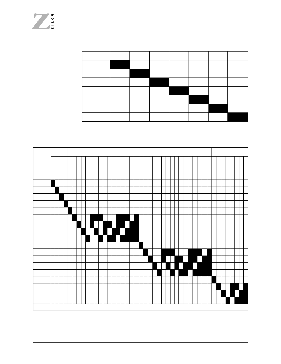
C
ONTROL
R
EGISTERS
P
ROGRAM
B
LOCKING
M
AP
40
Z86230--PRELIMINARY
PS000400-TVC0499
Table 31. MPAA Matrix (Use Content Advisory Rating Register
08h
)
G
PG
PG-13
R
NC-17
X
NR
G
PG
PG-13
R
NC-17
X
NR
T
ABLE
32. TV P
ARENTAL
G
UIDELINES
M
ATRIX
(U
SE
C
ONTENT
A
DVISORY
R
ATING
R
EGISTER
09h
,
0Ah
,
0Bh
)
Y Y7 G
PG
14
MA
≠ ≠ F
V
≠ ≠ V S L D V
S
V
L
V
D
S
L
S
D
L
D
V
S
L
V
S
D
V
L
D
S
L
D
V
S
L
D
≠ V S L D V
S
V
L
V
D
S
L
S
D
L
D
V
S
L
V
S
D
V
L
D
S
L
D
V
S
L
D
≠ V S L V
S
V
L
S
L
V
S
L
Y
Y7
Y7-FV
G
PG
PG-V
PG-S
PG-L
PG-D
14
14-V
14-S
14-L
14-D
MA
MA-V
MA-S
MA-L
N
OTE
: "≠" denotes a base rating.

P
ROGRAM
B
LOCKING
M
AP
C
ONTROL
R
EGISTERS
PS000400-TVC0499
Z86230--PRELIMINARY
41
T
ABLE
33. C
ANADIAN
E
NGLISH
M
ATRIX
(U
SE
C
ONTENT
A
DVISORY
R
ATING
R
EGISTER
0Fh
)
E
C
C8+
G
PG
14+
18+
E
C
C8+
G
PG
14+
18+
T
ABLE
34. C
ANADIAN
F
RENCH
M
ATRIX
(U
SE
C
ONTENT
A
DVISORY
R
ATING
R
EGISTER
10h
)
E
G
8ans+
13ans+
16ans+
18ans+
E
G
8ans+
13ans+
16ans+
18ans+

D
EMONSTRATION
P
ROGRAMS
C
OMMUNICATING
WITH
THE
Z86230
42
Z86230--PRELIMINARY
PS000400-TVC0499
7. DEMONSTRATION
PROGRAMS
7.1 C
OMMUNICATING
WITH
THE
Z86230
Communications with the Z86230 is accomplished using its serial communica-
tions interface (it is assumed that the user is familiar with the serial protocol
requirements).
N
OTE
:
In the following descriptions,
<ENTER> means "press the Enter key".
7.2 I
2
C O
PERATION
The Z86230 is configurable as an I
2
C slave device. The PC communicates with
the Z86230 through its parallel port. Though these programs are not intended as
examples of how to program the application they do provide a means of illustrat-
ing the serial control process and capability of the Z86230.
The three programs available are titled
IICO
,
SCRIPTI
and
XDSCAP
. These pro-
grams compile and run satisfactorily with the Z86230 in a test board. Compiled
versions are available on disk. Contact your local ZiLOG sales office for further
information on these programs.
7.3 IICO
P
ROGRAM
This program sends 1 byte to the Z86230 without checking the status of the
RDY
bit. The program returns the contents of the Serial Status Register
(
SSR
) after the
command is entered. When the program is active the screen displays:
IIC Command Byte >
The user may enter any valid 1-byte command such as
FBh
(
RESET
) or
00h
(
NOP
) and then hit the
ENTER
key. The screen then displays the byte entered and
the
SSR
contents as follows:
IIC Byte = 00
IIC Status =
83h
This example shows that the
NOP
command was entered. The
SSR
contents,
83h
,
indicate that the
RDY
,
FLD
, and
LOCK
bits are High, which implies that the serial
port is ready for further input, that the input video signal was in Field 1 at the time
the status was read, and that the part is operating in video lock mode.
The
IICO
program is exited by entering a Control+C (^C) character.
For example, entering the following two 1-byte commands displays the following:
Reset the part
FB, 00

G
ENERAL
C
OMMANDS
D
EMONSTRATION
P
ROGRAMS
PS000400-TVC0499
Z86230--PRELIMINARY
43
7.4 G
ENERAL
C
OMMANDS
7.5 SCRIPTI
P
ROGRAM
This program is designed to send any number of 1 or 2-byte commands to the
Z86230. The list of commands to be executed are contained in Script files that
have the extension
.SER
. For example, a file called
FILFA.SER
contains the 1-byte
command:
{C5, 02} * Set xds filter to all future class
The program is invoked by typing:
SI File_name <ENTER>
N
OTE
:
File_name without the
.SER extension.
The screen displays:
EEG CCD2 Serial Interface Script Player Version x.xx
Slave Address is
28h
Script File Done
The responding slave address is reported to the screen. When all of the commands
in the file are successfully sent to the Z86230, the PC returns to the system
prompt.
The program checks the
RDY
status before sending each byte. If, during the entry of
a command, the
RDY
bit is not found to be a
1
after an extended wait, the program
reports the contents of the
SSR
and then continues checking for
RDY
.
7.6 S
CRIPT
F
ILES
Script files can be generated to perform all of the setup and control functions
required to use the part in an application. The script files shown in the following
pages are examples used to set up the Z86230 for different operating conditions.
Some of the files contain only a single command while others include several
commands. The user should refer to
Z86230 Commands and Registers Summary
for details. Although the following examples are organized according to a particu-
lar register, some of the files contain information for several registers.
Serial Command
Command Code
RESET
FBh, FCh, 00h
NOP
00h
SSB
FFh,...FFh,FEh

D
EMONSTRATION
P
ROGRAMS
S
CRIPT
F
ILES
44
Z86230--PRELIMINARY
PS000400-TVC0499
7.6.1 Configuration Register Script Files
7.6.2 XDSCAP Program
This program performs the task of XDS data recovery. XDS recovery must first be
enabled through the appropriate XDS Filter command. Script file examples for
setting the XDS Filter are shown below.
The program is invoked by typing:
SI File_name <ENTER>
When the program is invoked, the PC screen displays:
EEG CCD2 XDS Data Recovery Test Program Version x.xx
Slave Address is
28h
The responding slave address is reported to the screen.
When communication is acknowledged, the program displays all XDS data recov-
ered from those packets that were enabled through the XDS Filter command:
{01,03}Current Program{00}{0F,7F}....etc
The ASCII characters are displayed as ASCII characters, while the nonprinting char-
acters are displayed by their Hex values within curly braces. Byte pairs, such as
Class, Type, are shown as pairs within the curly braces, separated by a comma, for
example: {01,03}.
If no data is received within approximately 45 seconds, the program times out,
reports
Data Not Available
, and exits.
N
OTE
:
The
XDSCAP
program can also be exited by entering a Control+C (^C) character.
T
ABLE
35. C
ONFIGURATION
R
EGISTER
S
CRIPT
F
ILES
File Name
Command
Function
FIGVH
{C7,00}
Set INT Mask register clear
{83,12}
Bit set ext V pulse for pos
FIGN
{C0,00}
Set config back to default state
FIGPAL
{C0,01}
Set config register to TVS=1. Changes VBI line to
L22 PAL.

S
CRIPT
F
ILES
D
EMONSTRATION
P
ROGRAMS
PS000400-TVC0499
Z86230--PRELIMINARY
45
7.6.3 XDS Filter Register Script Files
File Name
Command
Function
FILA
{C5,1F}
Set XDS filter to all
FIL0
{C5,00}
Set XDS filter to none; turns off XDS recovery
FILCA
{C5,01}
Set XDS filter to all current class
FILC
{C5,41}
Set XDS filter to current, in band class
FILFA
{C5,02}
Set XDS filter to all future class
FILCH
{C5,04}
Set XDS filter to channel class
FILM
{C5,08}
Set XDS filter for misc. info
FILTIME
{C5,28}
Set XDS filter time only
FILVCR
{C5,9E}
Set XDS filter vcr info

E
LECTRICAL
C
HARACTERISTICS
A
BSOLUTE
M
AXIMUM
R
ATINGS
1
46
Z86230--PRELIMINARY
PS000400-TVC0499
8. ELECTRICAL
CHARACTERISTICS
8.1 A
BSOLUTE
M
AXIMUM
R
ATINGS
1
8.2 S
TANDARD
T
EST
C
ONDITIONS
The characteristics listed below apply for standard test conditions as noted. All
voltages are referenced to Ground. Positive current flows into the referenced pin
(Figure 7).
Symbol
Parameter
Value
Unit
V
DD
DC Supply Voltage
≠0.5 to 6.0
V
V
IN
DC Input Voltage
≠0.5 to V
DD
+0.5
V
V
OUT
DC Output Voltage
≠0.5 to V
DD
+0.5
V
I
IN
C
AUTION
:
DC Input Current per Pin
+10
mA
I
OUT
DC Output Current per Pin
+20
mA
I
DD
DC Supply Current
+30
mA
P
D
Power Dissipation per Device
300
mW
T
STG
Storage Temperature
≠65 to +150
∫C
T
L
Lead Temperature, 1 mm from Case for 10
seconds
260
∫C
Notes:
1. Voltages referenced to V
SS
(A).
Maximum ratings are those values beyond which damage to the device may occur.
Functional operation should be restricted to the limits specified in the DC and AC Characteristics tables
or Pin Description section.
F
IGURE
7. S
TANDARD
T
EST
L
OAD
From Output
Under Test
150 pF
250 µ
µ
A
2.1 k
+5V

DC C
HARACTERISTICS
E
LECTRICAL
C
HARACTERISTICS
PS000400-TVC0499
Z86230--PRELIMINARY
47
8.3 DC
C
HARACTERISTICS
8.4 AC
AND
T
IMING
C
HARACTERISTICS
8.4.1 Composite Video Input
8.5 E
LECTRICAL
C
HARACTERISTICS
8.5.1 Non-Standard Video Signals
Non-standard video signals must have the following characteristics:
T
ABLE
36. DC C
HARACTERISTICS
--T
A
= 0∫C to +70∫C; V
DD
= +4.75V to +5.25V
Symbol
Parameter
Conditions
Min.
Max.
Unit
V
IL
Input Voltage Low
0
0.2 V
DD
V
V
IH
Input Voltage High
0.7 V
DD
V
DD
V
V
OL
Output Voltage Low
I
OL
= 1.00 mA
≠
0.4
V
V
OH
Output Voltage High
I
OH
= 0.75 mA
V
DD
≠0.4V
≠2
V
I
IL
Input Leakage
0V, V
DD
≠3.0
3.0
mA
I
DD
Supply Current
30
mA
Kf
VCO Gain
≠
TBD
MHz/V
I
LP
Loop Filter Current
≠
TBD
mA
T
ABLE
37. C
OMPOSITE
V
IDEO
I
NPUT
Parameter
Conditions
Amplitude
1.0V p-p ±3 dB
Polarity
Sync tips negative
Bandwidth
600 kHz
Signal Type
Interlaced
Max Input R
470 ohms
DC Offset
Signal must be AC-coupled with a minimum series
capacitance of 0.1 µF
T
ABLE
38. N
ON
-S
TANDARD
V
IDEO
S
IGNALS
Parameter
Conditions
Sync Amplitude
200 mV minimum
Vertical Pulse
Width
3H ±0.5H
Vertical Pulse Tilt
20 mV maximum

E
LECTRICAL
C
HARACTERISTICS
E
LECTRICAL
C
HARACTERISTICS
48
Z86230--PRELIMINARY
PS000400-TVC0499
8.5.2 HIN/XIN Signal Input
H Timing
Phase Step (Head Switch) ±10 µs maximum
Fh Deviation (long term) ±0.5% maximum
Fh p-p Deviation (short term) ±0.3% maximum
Vertical Sync
Signal
The internal sync circuits lock to all 525- or 625-line
signals that exhibit a vertical sync pulse that meets the
following conditions:
1.
It is at least 3H ±0.5H wide.
2.
It starts at the proper 2H boundary for its field.
3.
If equalizing pulse serrations are present, they
must be less than 0.125H in width.
Minimum Signal-
to-Noise
The Z86230 functions down to a 25 dB signal-to-noise
ratio (CCIR-weighted) with one error per row or better
at that level.
Ratio to Composite
Video
Input
Table 39. HIN/XIN Signal Input
Mode
Parameter
Conditions
1. HIN
Input
(Video Lock Mode)
Amplitude
CMOS level signal where Low
0.2 V
CC
Polarity
Any
Frequency
15,734.263 Hz @ 3%
(HIN Lock Mode)
Amplitude
CMOS level signal where Low
0.2 V
CC
Polarity
Any
Frequency
Same as Display Horizontal Flyback (HFB)
pulse
2. XIN
Input
(XTAL)
Frequency
32.768 KHz
Frequency
tolerance
±20ppm @ T
A
= 25C, CL = 12.5pF
(Clock)
Amplitude
CMOS level signal where Low
0.2 V
CC
Frequency
32.768 kHz ±2%
T
ABLE
38. N
ON
-S
TANDARD
V
IDEO
S
IGNALS
Parameter
Conditions

E
LECTRICAL
C
HARACTERISTICS
E
LECTRICAL
C
HARACTERISTICS
PS000400-TVC0499
Z86230--PRELIMINARY
49
8.5.3 Line 21 Input Parameters (at 1.0V p-p)
Line 21 must be in its proper position to the leading edge of the Vertical Sync sig-
nal.
T
ABLE
40. L
INE
21 I
NPUT
P
ARAMETERS
Parameter
Conditions
Code Amplitude
50 IRE*
Code Zero Level
5 IRE, +15 IRE relative to Back Porch
Start of Code
10.5 ±0.5 µs (measure from the midpoint of the leading
edge of the composite video Hsync pulse to the
midpoint of the rising edge of the first clock run-in
cycle.)
Start of the Data
3.972 ms, ≠0.00 µs, +0.30 µs (measure from the
midpoint of the falling edge of the most recent clock
run-in cycle to the midpoint of the rising edge of the
start bit.)
N
OTE
: *A relative unit of measure developed by the Institute of Radio Engineers (IRE).
One IRE equals 1/140th of the composite video signal's peak-to-peak voltage. IRE is
the former name of what is now known as the Institute of Electrical and Electronics
Engineers (IEEE).

A
PPLICATION
I
NFORMATION
R
EFERENCE
D
ESIGNS
50
Z86230--PRELIMINARY
PS000400-TVC0499
9. APPLICATION
INFORMATION
The recommended schematic, component placement, and PCB layout for a sin-
gle-sided DIP design are provided in the following figures. I
2
C communication
and
XTAL
mode are chosen in the reference circuit design. EMI and noise in the
video frequency range is kept to an absolute minimum by running the ground
plane underneath the entire Z86230 package length. This design is recommended
for both SOIC and DIP package styles.
9.1 R
EFERENCE
D
ESIGNS
F
IGURE
8. Z86230 R
EFERENCE
C
IRCUIT
.
SDA
SCLK
NRST
I
2
C SEL
LPF
CSYNC
VIDEO
13
14
15
4
1
PB
X
OUT
X
IN
V
DD
RREF
V
SS
V
SS
(A)
C6
C5
C7
R5
C3
R4
C4
R1
CA1
CB1
L1
+5V
5
3
7
8
9
12
10
6
11
I
2
C Bus
Y1 R2
R3
C1
C2
H SEL
+5V
2
Z86230
INTRO
17

R
EFERENCE
D
ESIGNS
A
PPLICATION
I
NFORMATION
PS000400-TVC0499
Z86230--PRELIMINARY
51
T
ABLE
41. R
ECOMMENDED
C
OMPONENT
V
ALUES
FOR
Z86230 R
EFERENCE
C
IRCUIT
Component
Value
Units
R1
10
K
R2
22
M
R3
470
K
R4
470
R5
6.8
K
C1
10
pF
C2
20
pF
C3
0.1
µF
C4
560
pF
C5
0.1
µF
C6
6800
pF
C7
0.068
µF
CA1
0.1
µF
CB1
0.1
µF
L1
bead
N/A
Y1
32.768
kHz
U1
Z86230
N/A
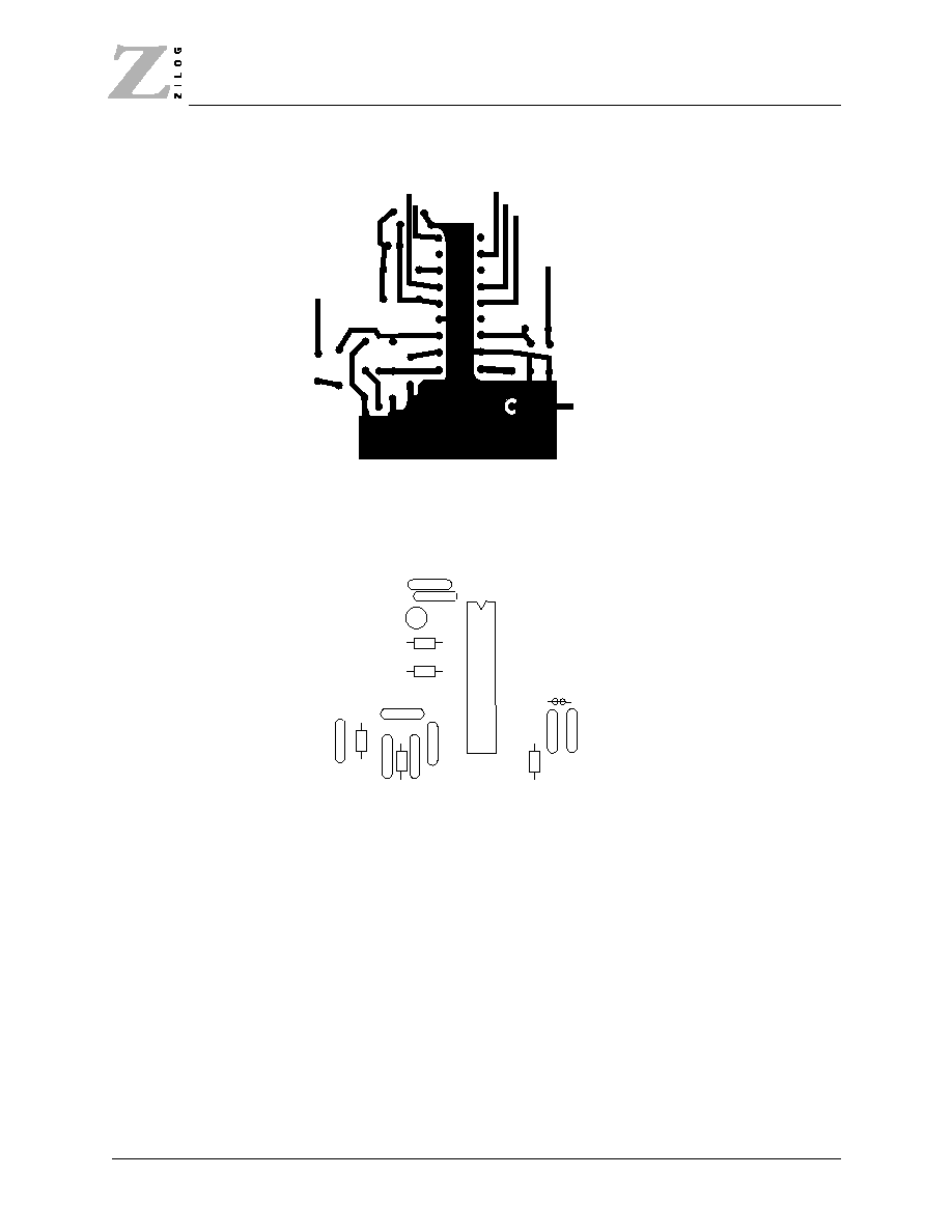
A
PPLICATION
I
NFORMATION
R
EFERENCE
D
ESIGNS
52
Z86230--PRELIMINARY
PS000400-TVC0499
F
IGURE
9. PCB D
ESIGN
OF
Z86230 R
EFERENCE
C
IRCUIT
VDD(+5V)
VSS
SCLK
SDA
NRST
VIDEO
C2
C1
Y1
C4
C5
C6
R5
C7
R4
C3
R1
CA1
CB1
L1
R3
R2
U1
INTRO
I
2
C SEL
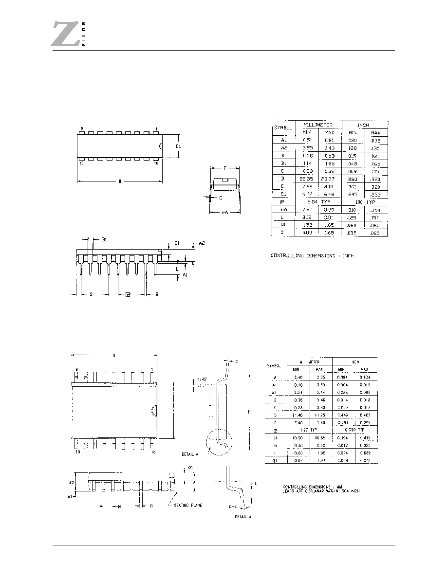
R
EFERENCE
D
ESIGNS
P
ACKAGING
PS000400-TVC0499
Z86230--PRELIMINARY
53
10. PACKAGING
F
IGURE
10. 18-L
EAD
DIP P
ACKAGE
D
IAGRAM
F
IGURE
11. 18-L
EAD
SOIC P
ACKAGE
D
IAGRAM

O
RDERING
I
NFORMATION
P
ART
N
UMBER
D
ESCRIPTION
54
Z86230--PRELIMINARY
PS000400-TVC0499
11. ORDERING
INFORMATION
For fast results, contact your local ZiLOG sale offices for assistance in ordering
the part(s) required.
11.1 P
ART
N
UMBER
D
ESCRIPTION
The ZiLOG part numbers consist of a number of components.
E
XAMPLE
:
Part number Z86230 12 P S C is a Z86230, 12-MHz DIP, 0∫C to +70∫C, Plastic
Standard Flow, and consists of the codes indicated in the following table.
Z86230 (12 MHz)
Standard Temperature
18-Pin DIP
18-Pin SOIC
Z8623012PSC
Z8623012SSC
Z
ZiLOG prefix
86230
Product Number
12
Speed (in MHz)
P
Package
S
Temperature
C
Environmental Flow

P
ART
N
UMBER
D
ESCRIPTION
P
RECHARACTERIZATION
P
RODUCT
PS000400-TVC0499
Z86230--PRELIMINARY
55
12. PRECHARACTERIZATION
PRODUCT
The product represented by this document is newly introduced and ZiLOG has not
completed the full characterization of the product. The document states what
ZiLOG knows about this product at this time, but additional features or non-con-
formance with some aspects of the document may be found, either by ZiLOG or
its customers in the course of further application and characterization work. In
addition, ZiLOG cautions that delivery may be uncertain at times, due to start-up
yield issues.
ZiLOG, Inc.
910 East Hamilton Avenue, Suite 110
Campbell, CA 95008
Telephone (408) 558-8500
FAX 408 558-8300
Internet:
http://www.zilog.com

C
USTOMER
F
EEDBACK
F
ORM
P
ART
N
UMBER
D
ESCRIPTION
56
Z86230--PRELIMINARY
PS000400-TVC0499
CUSTOMER FEEDBACK FORM
Z86230 P
RODUCT
S
PECIFICATION
If you experience any problems while operating this product, or if you note any
inaccuracies while reading this Product Specification, please copy and complete
this form, then mail or fax it to ZiLOG (see Return Information, below). We also
welcome your suggestions!
C
USTOMER
I
NFORMATION
P
RODUCT
I
NFORMATION
R
ETURN
I
NFORMATION
ZiLOG
System Test/Customer Support
910 E. Hamilton Avenue, Suite 110, MS 4≠3
Campbell, CA 95008
Fax: (408) 558-8536
Email: tools@zilog.com
P
ROBLEM
D
ESCRIPTION
OR
S
UGGESTION
Provide a complete description of the problem or your suggestion. If you are
reporting a specific problem, include all steps leading up to the occurrence of the
problem. Attach additional pages as necessary.
________________________________________________________________________
________________________________________________________________________
________________________________________________________________________
________________________________________________________________________
________________________________________________________________________
________________________________________________________________________
________________________________________________________________________
Name
Country
Company
Phone
Address
Fax
City/State/Zip
E-Mail
Serial # or Board Fab #/Rev. #
Software Version
Document Number
Host Computer Description/Type

PS000400-TVC0499
Z86230—PRELIMINARY
57
I
NDEX
N
UMERICS
14+-rated
. . . . . . . . . . . . . . . . . . . . . . . . . . . 33
18+-rated
. . . . . . . . . . . . . . . . . . . . . . . . . . . 33
18-Lead DIP Package
. . . . . . . . . . . . . . . . . 53
18-Lead SOIC Package
. . . . . . . . . . . . . . . . 53
2-wire bus
. . . . . . . . . . . . . . . . . . . . . . . . . . 18
3-byte
READ
. . . . . . . . . . . . . . . . . . . . . . . . 36
A
Absolute Maximum Ratings
. . . . . . . . . . . . 46
AC and Timing Characteristics
. . . . . . . . . . 47
Acknowledge
. . . . . . . . . . . . . . . 11, 18
-
19
,
22
Application Information
. . . . . . . . . . . . . . . 50
Architectural Overview
. . . . . . . . . . . . . . . . . 9
ASCII characters
. . . . . . . . . . . . . . . . . . . . . 44
Auto Clock Set
. . . . . . . . . . . . . . . . . . . . . . . 9
B
base rating
. . . . . . . . . . . . . . . . . . . . . . . 30
,
40
Basic Serial Commands
. . . . . . . . . . . . . . . 23
Block Diagram and Operational Overview
. . 9
Block Timer
. . . . . . . . . . . . . . . . . . . . . . . . 32
blocking
32, 39
Blocking Control Registers . . . . . . . . . . 32, 34
Blocking No Rating Programs
. . . . . . . . . . 17
Bus Conditions
. . . . . . . . . . . . . . . . . . . . . . 18
Bus Protocol
. . . . . . . . . . . . . . . . . . . . . . . . 18
busy bit
. . . . . . . . . . . . . . . . . . . . . . . . . . . . 11
Byte pairs
. . . . . . . . . . . . . . . . . . . . . . . . . . 44
C
C8+-rated
. . . . . . . . . . . . . . . . . . . . . . . . . . . 33
Call Letter
. . . . . . . . . . . . . . . . . . . . 20
,
27
,
36
Canadian English Language
Content Advisory
. . . . . . . . . . . . . . . . . . . 32
Canadian French Language
Content Advisory
. . . . . . . . . . . . . . . . . . . 33
CHAN
. . . . . . . . . . . . . . . . . . . . . . . . . . 26
,
39
Channel Information Class packets
. . . . . . . 26
CHKSUM
. . . . . . . . . . . . . . . . . . . . . . . . . . . 37
class type 2 packet
. . . . . . . . . . . . . . . . . . . . 20
class type 3 packet
. . . . . . . . . . . . . . . . . . . . 20
Class/Type system
. . . . . . . . . . . . . . . . . . . . 35
Clock and Data Transitions
. . . . . . . . . . . . . 21
Command Processor
. . . . . . . . . . . . . . . . . . 10
Commands
. . . . . . . . . . . . . . . . . . . . . . . . . 23
Communicating with the Z86230
. . . . . . . . 42
Comp Sync
. . . . . . . . . . . . . . . . . . . . . . . . . 10
Composite Video
. . . . . . . . . . . . . . . 9
,
14, 49
input
. . . . . . . . . . . . . . . . . . . . . . . 9, 10, 47
signal
. . . . . . . . . . . . . . . . . . . . . . . . . . . 10
Configuration Register
. . . . . . . . . . . . . . . . 25
Script Files
. . . . . . . . . . . . . . . . . . . . . . . 44
Content Advisory
packet
. . . . . . . . . . . . . . . . . . . 9
,
15
,
32
,
39
Rating registers
. . . . . . . . . . . . . . . . . . . . 39
Rating Select Register . . . . . . 15, 28-31, 33
Registers . . . . . . . . . . . . . . . . . . . . . . 31-32
CONTINUE
. . . . . . . . . . . . . . . . . . . . . . . . . 36
Control+C (^C)
. . . . . . . . . . . . . . . . . . . 42
,
44
Counting Circuits
. . . . . . . . . . . . . . . . . . . . 10
C-rated
. . . . . . . . . . . . . . . . . . . . . . . . . . . . 33
CSYNC
. . . . . . . . . . . . . . . . . . . . . . . . . 10
,
14
CURR
. . . . . . . . . . . . . . . . . . . . . . . . . . 26
,
39
Current Class
. . . . . . . . . . . . . . . . . . . . . . . . 36
packets
. . . . . . . . . . . . . . . . . . . . . . . 26
,
36
Program Rating data
. . . . . . . . . . . . . . . . 37
Customer Feedback Form
. . . . . . . . . . . . . . 56
Customer Information
. . . . . . . . . . . . . . . . . 56
D
D- and L-rated programs
. . . . . . . . . . . . . . . 31
data available flag
. . . . . . . . . . . . . . . . . . . . 36
data clock
. . . . . . . . . . . . . . . . . . . . . . . . . . 10
recovery circuits
. . . . . . . . . . . . . . . . . . . 10
Data Slicer
. . . . . . . . . . . . . . . . . . . . . . . . . . 10
Data Available Flag (
DAV
)
. . . . . . . . . . 25
,
39
DAV bit
. . . . . . . . . . . . . . . . . . . .20
-
21
,
35
-
36
DC Characteristics
. . . . . . . . . . . . . . . . . . . 47
DCLK
. . . . . . . . . . . . . . . . . . . . . . . . . . . . . . 10
phase lock
. . . . . . . . . . . . . . . . . . . . . . . . 10
Decoder Control circuit block
. . . . . . . . . . . 10
Demonstration Programs
. . . . . . . . . . . . . . 42
DIP
. . . . . . . . . . . . . . . . . . . . . . . . . . . . 13
,
54
DIP package
. . . . . . . . . . . . . . . . . . . . . . . . 50
Disclaimer
. . . . . . . . . . . . . . . . . . . . . . . . . . . 2
DLE
. . . . . . . . . . . . . . . . . . . . . . . . . . . . 27
-
28
dLOK
. . . . . . . . . . . . . . . . . . . . . . . . . . . 27
-
28
dXDS
. . . . . . . . . . . . . . . . . . . . . . . . . . . . . . 27

58
Z86230—PRELIMINARY
PS000400-TVC0499
E
EIA≠608
. . . . . . . . . . . . . . . . . . . . . . . . . . . 36
EIA≠608A
. . . . . . . . . . . . . . . . . . . . . 9
,
35
,
37
EIA-744A
. . . . . . . . . . . . . . . . . . . . . . . . . . . 9
Electrical Characteristics
. . . . . . . . . . . . 46
-
47
Electronics Industry Association
. . . . . . . . . . 9
EMI
. . . . . . . . . . . . . . . . . . . . . . . . . . . . . . . 50
END
. . . . . . . . . . . . . . . . . . . . . . . . . . . . . . . 36
END packet
. . . . . . . . . . . . . . . . . . . . . . . . . 37
EOF
. . . . . . . . . . . . . . . . . . . . . . . . . . . . 27
-
28
E-rated
. . . . . . . . . . . . . . . . . . . . . . . . . . . . . 34
Extended Data Services
. . . . . . . . . . . . . . 9
,
35
F
Field 1
. . . . . . . . . . . . . . . . . . . . . . . 25
,
27, 42
Field 2
. . . . . . . . . . . . . . . 9
,
25
,
27
,
35
,
36
-
37
field counter
(
FLD CNTR
) . . . . . . . . . . . . . . 10
FLD
. . . . . . . . . . . . . . . . . . . . . . . . . 25
,
39
,
42
fully programmable
. . . . . . . . . . . . . . . . . 9
,
17
FUTR
. . . . . . . . . . . . . . . . . . . . . . . . . . . 26
,
39
Future Class packets
. . . . . . . . . . . . . . . . . . 26
G
General Commands
. . . . . . . . . . . . . . . . . . . 43
G-rated
. . . . . . . . . . . . . . . . . . . . . . . 28
,
33
-
34
H
H Lock
. . . . . . . . . . . . . . . . . . . . . . . . . . . . . 17
H SEL
. . . . . . . . . . . . . . . . . . . . . . . . . . . . . 13
H signal
. . . . . . . . . . . . . . . . . . . . . . . . . . . . 10
Hex values
. . . . . . . . . . . . . . . . . . . . . . . . . . 44
HIN
Input
. . . . . . . . . . . . . . . . . . . . . . . . . . . . 48
Lock Mode
. . . . . . . . . . . . . . . . . . . . . . . 48
mode
. . . . . . . . . . . . . . . . . . . . . . . . . 13
-
14
HIN/XIN
. . . . . . . . . . . . . . . . . . . . . . . 9
,
13
-
14
input signal
. . . . . . . . . . . . . . . . . . . . . . . 10
Signal Input
. . . . . . . . . . . . . . . . . . . . . . . 48
Horizontal (H) Lock circuit
. . . . . . . . . . . . . 10
horizontal frequency signal
. . . . . . . . . . . . . 14
horizontal timing signal
. . . . . . . . . . . . . . 9
-
10
I
I
2
C Bus
. . . . . . . . . . . . . . . . . . . . . . . . . . . . 20
interface
. . . . . . . . . . . . . . . . . . . . . . . . . 19
Operation
. . . . . . . . . . . . . . . . . . . . . . . . 18
I
2
C communication
. . . . . . . . . . . . . . . . . . . 50
I
2
C master
. . . . . . . . . . . . . . . . . . . . . . . 15
,
21
I
2
C Operation
. . . . . . . . . . . . . . . . . . . . . . . 42
I
2
C SEL
. . . . . . . . . . . . . . . . . . . . . . 13
,
16
,
18
I
2
C serial
communication port
. . . . . . . . . . . . . . 9
,
17
control interface
. . . . . . . . . . . . . . . . . . . 16
timing
. . . . . . . . . . . . . . . . . . . . . . . . . . . 22
I
2
C slave device
. . . . . . . . . . . . . . . . . . . . . 42
I
2
C START condition
. . . . . . . . . . . . . . . . . 19
I
2
C STOP condition
. . . . . . . . . . . . . . . . . . 19
IICO Program
. . . . . . . . . . . . . . . . . . . . . . . 42
Impulse Capture
. . . . . . . . . . . . . . . . . . 27
,
36
indirect addressing
. . . . . . . . . . . . . . . . . . . 11
Input Signals
. . . . . . . . . . . . . . . . . . . . . . . . . 9
Internal Registers
. . . . . . . . . . . . . . . . . 20, 39
Interrupt
Mask Register
. . . . . . . . . . . . . . . . . . 15
,
28
Output
. . . . . . . . . . . . . . . . . . . . . . . . . . . 15
Request Register
. . . . . . . . . . . . . . . . . . . 27
INTR
. . . . . . . . . . . . . . . . . . . . . . . . . . . 25
,
39
INTRO
. . . . . . . . . . . . . . . . . . . . . . . . . . . . . 15
L
Least Significant Bit
(
LSB
) . . . . . . . . . . . . . 18
Line 21
. . . . . . . . . . . . . . . . . . . . . . . . . . 9
,
16
Activity Register
. . . . . . . . . . . . . . . . . . . 27
field 2
. . . . . . . . . . . . . . . . . . . . . . . . . . . 37
Input Parameters
. . . . . . . . . . . . . . . . . . . 49
Program Rating information
. . . . . . . . . . 36
line counter
(
LINE CNTR
) . . . . . . . . . . . . . . 10
Local Time Zone
. . . . . . . . . . . . . . . . . . 27
,
36
LOCK
. . . . . . . . . . . . . . . . . . . . . 25
,
27
,
39
,
42
Loop Filter
(
LPF
) . . . . . . . . . . . . . . . . . . 15
,
47
LTZ
. . . . . . . . . . . . . . . . . . . . . . . . . . . . 27
,
36
M
master device
. . . . . . . . . . . 18
-
19
,
21
,
27
,
36
MISC
. . . . . . . . . . . . . . . . . . . . . . . . . . . 26
,
39
Miscellaneous Class
data
. . . . . . . . . . . . . . . . . . . . . . . . . . . . . 36
packets
. . . . . . . . . . . . . . . . . . . . . . . . . . 26
MPAA
Content Advisory
. . . . . . . . . . . . . . . . . . 28
Rating
. . . . . . . . . . . . . . . . . . . . . . . . . . . 29
Ratings standards
. . . . . . . . . . . . . . . . . . 28
N
No Connect (NC) . . . . . . . . . . . . . . . . . . . . . 15

PS000400-TVC0499
Z86230—PRELIMINARY
59
NC-17-rated
. . . . . . . . . . . . . . . . . . . . . . . . . 28
Net ID
. . . . . . . . . . . . . . . . . . . . . . . . . . 27
,
36
no operation
(NOP) . . . . . . . . . . . . . . . . . . . 23
Non-Standard Video Signals
. . . . . . . . . . . . 47
NOP command
. . . . . . . . . . . . . . . . . . . 23
,
42
Not Acknowledge
(NACK) . . . . . . . 19
,
21
-
22
Not Busy
. . . . . . . . . . . . . . . . . . . . . . . . . . . 18
Not Rated
. . . . . . . . . . . . . . . . . . . . . . . 28
,
39
NRST
. . . . . . . . . . . . . . . . . . . . . . . . . . . . . . 13
NTSC
. . . . . . . . . . . . . . . . . . . 9
,
14
,
16
-
17
,
26
NTSC Line 21
. . . . . . . . . . . . . . . . . . 9
,
16
,
26
O
Ordering Information
. . . . . . . . . . . . . . . . . 54
Out-of-Band Channel Number packets
. 27
,
36
P
Packaging
. . . . . . . . . . . . . . . . . . . . . . . . . . 53
PAL
. . . . . . . . . . . . . . . . . . . . 9
,
16
-
17
,
26
,
44
Part Number Description
. . . . . . . . . . . . . . . 54
PB
. . . . . . . . . . . . . . . . . . . . . . . . 9
,
15
-
16, 32
PG-13-rated
. . . . . . . . . . . . . . . . . . . . . . . . . 28
PG-rated
. . . . . . . . . . . . . . . . . . . . . . . . 28
,
33
Picture-In-Picture
(PiP) . . . . . . . . . . . . . . . . . 9
Pin Descriptions
. . . . . . . . . . . . . . . . . . . . . 13
Power Supply
. . . . . . . . . . . . . . . . . . . . . . . 15
Precharacterization
. . . . . . . . . . . . . . . . . . . 55
Problem Description
. . . . . . . . . . . . . . . . . . 56
Product Information
. . . . . . . . . . . . . . . . . . 56
Program Blocking
. . . . . . . . . . . . . . . . . 15
-
17
Data Packet Recovery
. . . . . . . . . . . . . . . 36
Map
. . . . . . . . . . . . . . . . . . . . . . . . . . . . . 39
registers
. . . . . . . . . . . . . . . . . . . . . . . . . . 20
Signal
. . . . . . . . . . . . . . . . . . . . . . . . . . . . 9
Program Rating information
. . . . . . . . . 36
-
37
Program Rating XDS filter
. . . . . . . . . . . . . 37
Program Unblock Hold Off
. . . . . . . . . . . . . 17
program-blocking response
. . . . . . . . . . . . . 39
PUBL
. . . . . . . . . . . . . . . . . . . . . . . . . . . 26
,
39
Public Service Class
. . . . . . . . . . . . . . . . . . 26
R
RBS
. . . . . . . . . . . . . . . . . . . . . .20
,
23
,
36
,
38
RDS1
. . . . . . . . . . . . . . . . . . . . . . . . . . . 20
,
38
RDS2
. . . . . . . . . . . . . . . . . . . . . . . . . . . 20
,
38
RDY
. . . . . . . . . . . . . . . . . .20
,
23
,
25
,
38
,
39
bit
. . . . . . . . . . . . . . . . . . 19
,
23
,
38
,
42
-
43
status
. . . . . . . . . . . . . . . . . . . . . . 23
,
38
,
43
READ
. . . . . . . . . . . . . . . . . . 11
,
13
,
18
-
19
,
25
and
WRITE
Commands
. . . . . . . . . . . . . . 23
Bank 0 mode
. . . . . . . . . . . . . . . . . . . . . . 36
Bank Select
. . . . . . . . . . . . . . . . . . . . 20
,
23
SELECT
. . . . . . . . . . . . . . . . . . . . 20
,
23
,
35
sequence
. . . . . . . . . . 11
,
20
-
21
,
23
-
24
,
38
Reading Data Using the I
2
C Bus
. . . . . . . . 20
Reference Designs
. . . . . . . . . . . . . . . . . . . 50
Registers Summary
. . . . . . . . . . . . . . . . . . . 25
RESET
. . . . . . . . . . . 13
,
17
,
23
,
25
,
38
,
42
-
43
RESET
state
. . . . . . . . . . . . . . . . . . . . . . . . . 26
Resistor Reference
. . . . . . . . . . . . . . . . . . . 15
Return Information
. . . . . . . . . . . . . . . . . . . 56
ROVR
. . . . . . . . . . . . . . . . . . . . . . . . . . 25
,
39
R-rated
. . . . . . . . . . . . . . . . . . . . . . . . . . . . 28
RREF
. . . . . . . . . . . . . . . . . . . . . . . . . . . . . . 15
S
S- and V-rated programs
. . . . . . . . . . . . . . . 30
SCLK
. . . . . . . . . . . . . . . 15
-
16
,
18-19
,
21
-
22
Script Files
. . . . . . . . . . . . . . . . . . . . . . 43
-
45
SCRIPTI
. . . . . . . . . . . . . . . . . . . . . . . . . . . 42
SDA
. . . . . . . . . . . . . . . . . . . . . . 15
,
19
,
21
-
22
SDA
line
. . . . . . . . . . . . . . . . . . . . . . . . . . . 18
serial clock
. . . . . . . . . . . . . . . . . . . . . . 15, 18
Serial Communications Interface
. . . . . 18, 42
Serial Control
port
. . . . . . . . . . . . . . . . . . . . . . . . . . . . . 26
process
. . . . . . . . . . . . . . . . . . . . . . . . . . 42
Serial Data
. . . . . . . . . . . . . . . . . . . . . . . . . . 15
serial port
. . . . . . . . . . . . . . . . . 16
,
23
,
38
,
42
Serial Status Register
(
SSR
) . . . . 19, 21, 23
,
25, 27, 35, 38
,
42-43
DAV bit
. . . . . . . . . . . . . . . . . . . . . . . . . 21
single-sided DIP design
. . . . . . . . . . . . . . . 50
slave address
. . . . . . . . . .9
,
11
,
13
,
16
,
18
,
44
READ
. . . . . . . . . . . . . . . . . . . . . . . . 18
-
19
WRITE
. . . . . . . . . . . . . . . . . . . . . . . . 18
-
19
slave device
. . . . . . . . . . . . . . . . . . . . . . . . . 18
slice level
. . . . . . . . . . . . . . . . . . . . . . . . . . 10
SOIC
. . . . . . . . . . . . . . . . . . . . . . . . . . . 13
,
54
SOIC package
. . . . . . . . . . . . . . . . . . . . . . . 50
SSB
. . . . . . . . . . . . . . . . . . . . . . . . . 21
,
36
,
43
Standard Test Conditions
. . . . . . . . . . . . . . 46
START
. . . . . . . . . . . . . . . . . . . . . . . . . . . . 18
condition
. . . . . . . . . . . . . . . . . . . 18
-
19
,
21
packet
. . . . . . . . . . . . . . . . . . . . . . . . . . . 37

60
Z86230—PRELIMINARY
PS000400-TVC0499
Status register
data
. . . . . . . . . . . . . . . . . . . . . . . . . . . . . 19
RDY bit
. . . . . . . . . . . . . . . . . . . . . . . . . . 20
STOP condition
. . . . . . . . . . . . . . . . 18
,
21-22
Sync slice level
. . . . . . . . . . . . . . . . . . . . . . 14
Sync Slicer
. . . . . . . . . . . . . . . . . . . . . . . . . 10
T
Tape Delay
. . . . . . . . . . . . . . . . . . . . . . 27
,
36
Television Decoder Circuits Act of 1990
. . . 9
television VBI
. . . . . . . . . . . . . . . . . . . . . . . . 9
The I
2
C Bus Protocol
. . . . . . . . . . . . . . . . . 18
Time of Day
(TOD) . . . . . . . . . . . . . . . . 27
,
36
Timing and Counting Circuits
. . . . . . . . . . . 10
Timing Characteristics
. . . . . . . . . . . . . . . . 47
TV Parental Guidelines
. . . . . . . . . . . . . . . . 29
Rating matrix
. . . . . . . . . . . . . . . . . . . . . 39
Ratings standards
. . . . . . . . . . . . . . . 29
-
30
TV-14-L-rated
. . . . . . . . . . . . . . . . . . . . . . . 31
TV-14-rated
. . . . . . . . . . . . . . . . . . . . . . . . . 29
TV-14-S-rated
. . . . . . . . . . . . . . . . . . . . . . . 30
TV-14-V-rated
. . . . . . . . . . . . . . . . . . . . . . . 30
TV-G-rated
. . . . . . . . . . . . . . . . . . . . . . . . . 29
TV-MA-L-rated
. . . . . . . . . . . . . . . . . . . . . . 31
TV-MA-rated
. . . . . . . . . . . . . . . . . . . . . . . 29
TV-MA-S-rated
. . . . . . . . . . . . . . . . . . . . . . 30
TV-MA-V-rated
. . . . . . . . . . . . . . . . . . . . . 30
TV-NONE-rated
. . . . . . . . . . . . . . . . . . . . . 29
TV-PG-D-rated
. . . . . . . . . . . . . . . . . . . . . . 31
TV-PG-L-rated
. . . . . . . . . . . . . . . . . . . . . . 31
TV-PG-rated
. . . . . . . . . . . . . . . . . . . . . . . . 29
TV-PG-S-rated
. . . . . . . . . . . . . . . . . . . . . . 30
TV-PG-V-rated
. . . . . . . . . . . . . . . . . . . . . . 30
TVS
. . . . . . . . . . . . . . . . . . . . . . . . . . . . . . . 26
TV-Y7-FV-rated
. . . . . . . . . . . . . . . . . . . . . 30
TV-Y7-rated
. . . . . . . . . . . . . . . . . . . . . . . . 29
TV-Y-rated
. . . . . . . . . . . . . . . . . . . . . . . . . 29
V
VBI Data Processing
. . . . . . . . . . . . . . . . . . 16
VBI line
. . . . . . . . . . . . . . . . . . . . . . . . . . . . 44
V-Chip
. . . . . . . . . . . . . . . . . . . . . . . . . . . . . . 9
VCO Gain
. . . . . . . . . . . . . . . . . . . . . . . . . . 47
VCO Lock
. . . . . . . . . . . . . . . . . . . . . . . . . . 17
V
DD
. . . . . . . . . . . . . . . . . . . . . . . . . . . . . . . 15
Vertical Blanking Interval
(VBI) . . . . . . . . . . 9
VIDEO
. . . . . . . . . . . . . . . . . . . . . . . . . . . . . 14
Video
Input Signal Processing
. . . . . . . . . . . . . 10
Lock Mode
. . . . . . . . . . . . . . . . . . . . 42, 48
Standard
. . . . . . . . . . . . . . . . . . . . . . . . . 17
violence blocking
. . . . . . . . . . . . . . . . . . . . . 9
Voltage/Current Reference
. . . . . . . . . . . . . 11
Voltage-Controlled Oscillator
(VCO) . . . . . 10
V
SS
. . . . . . . . . . . . . . . . . . . . . . . . . . . . . . . 14
V
SS
(A)
. . . . . . . . . . . . . . . . . . . . . . . . . . . . . 15
W
WOVR
. . . . . . . . . . . . . . . . . . . . . . . . . . 25
,
39
WRITE
. . . . . . . . 11
,
13
,
18
-
20
,
23
-
24
,
35
,
38
addressing
. . . . . . . . . . . . . . . . . . . . . . . . 11
sequence
. . . . . . . . . . . . . . . . . . . . . . 11
,
20
Writing to the I
2
C Bus
. . . . . . . . . . . . . . . . 19
Writing to the Z86230
. . . . . . . . . . . . . . . . . 24
WRxx
. . . . . . . . . . . . . . . . . . . . . . . . . . 24
,
38
X
XDS
. . . . . . . . . . . . . . . . . . . . . . . . . . . . 9
,
35
activity
. . . . . . . . . . . . . . . . . . . . . . . . . . 27
class and type
. . . . . . . . . . . . . . . . . . . . . 36
Content Advisory packet
. . . . . . . . . . . . . 9
data
. . . . . . . . . . . . . . . 9
-
10
,
16
,
26
-
27
,
36
Data Activity
. . . . . . . . . . . . . . . . . . . . . 39
Data Activity Register
. . . . . . . . . . . . . . 26
Data Output
. . . . . . . . . . . . . . . . . . . . . . 17
data packets
. . . . . . . . . . . . . . . . . . . . 9
,
36
data recovery
. . . . . . . . . . . .24
,
27
, 35,
44
data stream
. . . . . . . . . . . . . . . . . . . . . . . 36
decoding
. . . . . . . . . . . . . . . . . . . . . . . . . 35
Filter
. . . . . . . . . . . . . . . . . . . . 9, 36-37, 39
Filter command
. . . . . . . . . . . . . . . . . . . . 44
Filter Register
. . . . . . . . . . . . . . . 24
,
35
-
37
Filter Register Script Files
. . . . . . . . . . . 45
filtering
. . . . . . . . . . . . . . . . . . . . . . . . . . 35
Network Name and Call Letter data
. . . . 20
packets
. . . . . . . . . . . . . . . . . . . . . . . . . . 36
Program Name data
. . . . . . . . . . . . . . . . 20
recovery
. . . . . . . . . . . . . . . . . . . . . . . . . 26
XDSCAP
. . . . . . . . . . . . . . . . . . . . . . . . . . . 42
XDSCAP Program
. . . . . . . . . . . . . . . . . . . 44
XIN
Input
. . . . . . . . . . . . . . . . . . . . . . . . . . . 48
XOUT
. . . . . . . . . . . . . . . . . . . . . . . . . . . . . 13
X-rated
. . . . . . . . . . . . . . . . . . . . . . . . . . . . 28

PS000400-TVC0499
Z86230—PRELIMINARY
61
XTAL
. . . . . . . . . . . . . . . . . . . . . . . . . . . . 9
,
48
circuit
. . . . . . . . . . . . . . . . . . . . . . . . . . . 13
In
. . . . . . . . . . . . . . . . . . . . . . . . . . . . . . . 14
mode
. . . . . . . . . . . . . . . . . . . . . . . . . 14
,
50
Output
. . . . . . . . . . . . . . . . . . . . . . . . . . . 13
Z
Z86230 Feature Set
. . . . . . . . . . . . . . . . . . . 16
Z86230 output registers
. . . . . . . . . . . . . . . 21
Z86230 Reference Circuit
. . . . . . . . . . . 50
-
52
Z86230 register address
. . . . . . . . . . . . 24
,
38
Z86230 WRITE commands
. . . . . . . . . . . . 35