 | –≠–ª–µ–∫—Ç—Ä–æ–Ω–Ω—ã–π –∫–æ–º–ø–æ–Ω–µ–Ω—Ç: Z86250 | –°–∫–∞—á–∞—Ç—å:  PDF PDF  ZIP ZIP |

1
Z86250
CP96TEL0302
CP96TEL0302 (2/96)
Z86250
STARSIGHT DATABASE ENGINE
FEATURES
s
Part
Package Speed (MHz)
Z86250
84-Pin PLCC
2 4
s
4.3- to 5.5-Volt Operating Range
s
0
∞
C to +70
∞
C Temperature Range
s
Low-Power Consumption
s
Segmented Base Registers
s
Infrared Receiver Logic
s
CRC-32 Encoding and Decoding Logic
s
Watch-Dog Timer (WDT) for Error Recovery
s
Serial I.M. and I
2
C Compatible Bus for External
Communication
s
Test Multiplexer for Chip Debug
For fast memory data manipulation, the Z86250 offers
segmented base registers. The device also features
PSRAM memory control and refresh logic.
The DBE is optimized to work with Zilog's Z89300 series of
TV controller devices to provide a cost-effective solution
for StarSight programming-guide data extraction and
display.
Zilog's Z86250 StarSight Data Base Engine (DBE) is
designed to process extracted data for the StarSight
on-screen programming guide. The device is logically
equivalent to the DBE1200 for StarSight applications.
The Z86250 provides a number of important peripheral
functions, such as the IR Blaster to send command signals
to the VCR, and low-power management to avoid loss of
d a t a .
Notes:
All Signals with a preceding front slash, "/", are active Low, e.g.:
B//W (WORD is active Low); /B/W (BYTE is active Low, only).
Power connections follow conventional descriptions below:
Connection
Circuit
Device
Power
V
CC
V
DD
Ground
GND
V
SS
GENERAL DESCRIPTION
C
USTOMER
P
ROCUREMENT
S
PECIFICATION
2
Z86250
CP96TEL0302
GENERAL DESCRIPTION
(Continued)
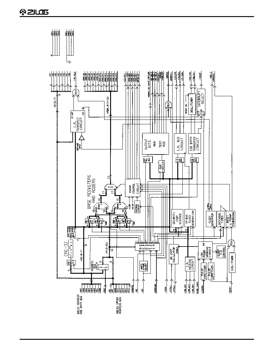
Database Engine Block Diagram

3
Z86250
CP96TEL0302
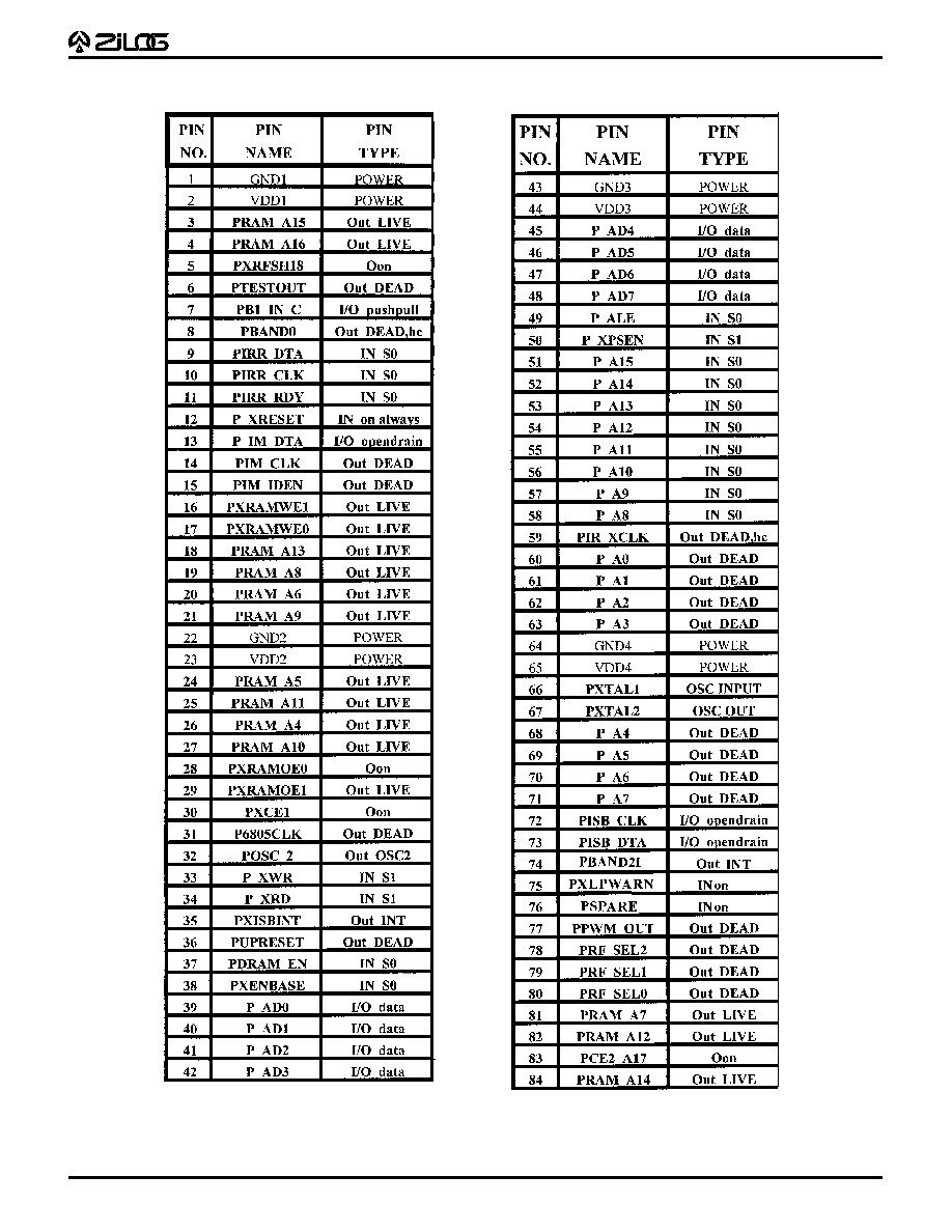
PIN DESCRIPTION
Z86250 84-Pin PLCC
Pin Assignments
PIRR/RDY
PIRR/CLK
PIRRDT
A
PB1/INC
PTEST
OUT
PXRFSH18
PRAM/A16
PRAM/A15
VDD
PRAM/A14
PCE2/A17
PRAM/A12
PRAM/A7
PRF/SEL0
PERF/SEL1
PPERF/SEL
2
PPWM/OUT
PSP
ARE
PXLPW
ARN
PBANDO
1 84
Z86250
84-Pin PLCC
33
42 43
32
53
54
11
75
74
PXRAMOE0
PX/RESET
P/IM/DATA
PIM/CLK
PXRAMWE1
PXRAMWE0
PRAM/A13
PRAM/A8
PRAM/A6
PRAM/A9
GND2
VDD2
PRAM/A5
PRAM/A11
PRAM/A4
PRAM/A10
PXRAMOE1
PXCE1
P6805CLK
POSC/2
PBAND2I
PISB/DTA
PISB/CLK
P/A7
P/A6
P/A5
P/A4
PXTAL1
VDD4
GND4
P/A3
P/A2
P/A1
P/A0
PIR/XCLK
P/A8
P/A9
P/A10
P/A11
P/A12
PXTAL2
P/A13
P/A14
P/A15
P/XPSEN
P/ALE
P/AD7
P/AD6
P/AD5
P/AD4
VDD3
GND3
P/AD3
P/AD2
P/AD1
P/AD0
PXENBASE
P
DRAM/EN
PUPRESET
PXISBINT
P/XRD
P/XWR
PIMI/DEN
12
GND
4
Z86250
CP96TEL0302
Z86250 Pinouts
PIN DESCRIPTION
(Continued)
5
Z86250
CP96TEL0302
ABSOLUTE MAXIMUM RATINGS
Symbol
Parameter
Min
Max
Units
Conditions
V
DD
Power Supply Voltage
≠0.3
7
V
All pins with respect to GND
T
A
Operating Ambient Temp.
0
7 0
∞
C
T
S
Storage Temperature
≠65
150
∞
C
Stress greater than those listed under Absolute Maximum
Ratings may cause permanent damage to the device. This
is a stress rating only; operation of the device at any
condition above those indicated in the operational sec-
tions of these specifications is not implied. Exposure to
absolute maximum rating conditions for extended periods
may affect device reliability.
6
Z86250
CP96TEL0302
DC CHARACTERISTICS
T
A
= 0
∞
C to + 70
∞
C; V
CC
= 4.3 V to + 5.5 V
Symbol
Parameter
Min
Max
Typical
Units
Conditions
Notes
V
IL
Input Voltage Low
0
0.2 V
DD
0.4
V
(except XTAL1)
V
IH
Input Voltage High
0.5 V
DD
V
DD
3.6
V
(except XTAL1)
V
OL1
Output Voltage Low
0.16
0.4
V
@ I
OH1
V
OH1
Output Voltage High
V
DD
≠0.4
4.75
V
DD
V
@ I
OH1
V
OL2
Output Voltage Low
0.16
0.4
V
@ I
OH2
V
OH2
Output Voltage High
V
DD
≠0.4
4.75
V
DD
V
@ I
OH2
VX
IL1
Input Voltage Low
0.2 V
DD
V
for XTAL1
VX
IH1
Input Voltage High
0.7 V
DD
V
for XTAL1
VX
OL2
Output Voltage Low
0.16
0.4
V
for XTAL2
@ 4.5 mA
VX
OH2
Output Voltage High
V
DD
≠0.4
4.75
V
DD
V
for XTAL2
@ 3.7 mA
I
OL1
Output Current Low
2.5
mA
I
OL1
Output Current High
1.5
mA
I
OL2
Output Current Low
1 0
mA
I
OL2
Output Current High
6
mA
V
DD1
Operating Supply Voltage
4.3
5.0
5.5
V
V
DD2
Sleep Supply Voltage
3.0
5.5
V
I
DD1
Operating Supply Current
40
mA
I
DD2
Operating Supply Current
10
µ
A
AC CHARACTERISTICS
T
A
= 0
∞
C to + 70
∞
C; V
DD
= 4.3 V to + 5.5 V
Symbol
Parameter
Min
Max
Typical
Units
Conditions
Notes
fosc
Oscillator Frequency
24
MHz
V
IN
Absolute Min/Max
Input Voltage Range
≠0.3
V
DD
+ 0.3
V
V
OUT
Absolute Min/Max
Output Voltage Range
≠0.3
V
DD
+ 0.3
V
7
Z86250
CP96TEL0302
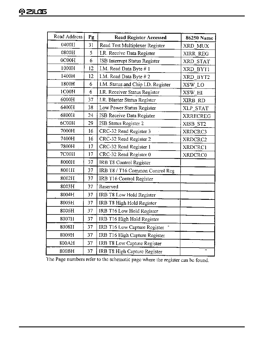
I/O READ ADDRESS REGISTER SUMMARY
I/O Read Address Register Summary
Table
8
Z86250
CP96TEL0302
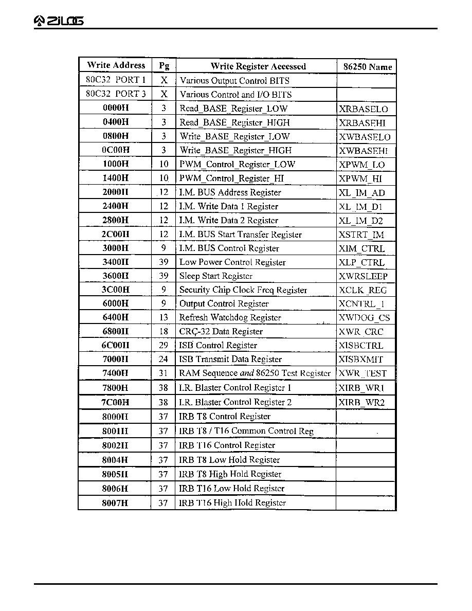
I/O WRITE ADDRESS REGISTER SUMMARY
I/O Write Address Register Summary
Table

9
Z86250
CP96TEL0302
Zilog's products are not authorized for use as critical compo-
nents in life support devices or systems unless a specific written
agreement pertaining to such intended use is executed between
the customer and Zilog prior to use. Life support devices or
systems are those which are intended for surgical implantation
into the body, or which sustains life whose failure to perform,
when properly used in accordance with instructions for use
provided in the labeling, can be reasonably expected to result in
significant injury to the user.
Zilog, Inc. 210 East Hacienda Ave.
Campbell, CA 95008-6600
Telephone (408) 370-8000
FAX 408 370-8056
Internet: http://www.zilog.com
© 1996 by Zilog, Inc. All rights reserved. No part of this document
may be copied or reproduced in any form or by any means
without the prior written consent of Zilog, Inc. The information in
this document is subject to change without notice. Devices sold
by Zilog, Inc. are covered by warranty and patent indemnification
provisions appearing in Zilog, Inc. Terms and Conditions of Sale
only. Zilog, Inc. makes no warranty, express, statutory, implied or
by description, regarding the information set forth herein or
regarding the freedom of the described devices from intellectual
property infringement. Zilog, Inc. makes no warranty of mer-
chantability or fitness for any purpose. Zilog, Inc. shall not be
responsible for any errors that may appear in this document.
Zilog, Inc. makes no commitment to update or keep current the
information contained in this document.