 | –≠–ª–µ–∫—Ç—Ä–æ–Ω–Ω—ã–π –∫–æ–º–ø–æ–Ω–µ–Ω—Ç: Z86317 | –°–∫–∞—á–∞—Ç—å:  PDF PDF  ZIP ZIP |
1
P R E L I M I N A R Y
Z86317
CMOS Z8
Æ
8-B
IT
MCU
DS96KEY1102
P
RELIMINAR
Y
C
USTOMER
P
ROCUREMENT
S
PECIFICA
TION
FEATURES
Part
ROM
RAM*
Speed
I/O
Package
Number (KB)
(Bytes)
(MHz)
(18-Pin)
Z86317
2
124
4
13
DIP, SOIC
Z86317
CMOS Z8
Æ
8-B
IT
M
ICROCONTROLLER
s
P24-P27 Can be Configured as a Voltage Divider
During Input Mode
s
On-Chip Precision RC Oscillator (Tolerance =
±
10%)
s
Fast Instruction Pointer: 1.5
µ
s @ 4 MHz
s
ESD Protection Circuitry
s
Hardwired Watch-Dog Timer (WDT)
GENERAL DESCRIPTION
The Z86317 device provides two on-chip 8-bit program-
mable counter/timers with a large number of user-select-
able modes. Each counter/timer is driven by its own 6-bit
programmable prescaler. The Z86317 counter/timers
offload system real-time tasks such as counting/timing
and input/output data communications for increased sys-
tem efficiency.
Notes:
All Signals with a preceding front slash, "/", are active Low, e.g.; B//W
(WORD is active Low); /B/W (BYTE is active Low, only).
Power connections follow conventional descriptions below:
Connection
Circuit
Device
Power
V
CC
V
DD
Ground
GND
V
SS
The Z86317 is a member of the Z8
Æ
family of CMOS
microcontrollers architected to be used in mouse applica-
tions. These devices offer on-board pull-up and pull-down
resistors, a scalable trip-point buffer to accommodate
opto-transistor outputs, and high drive ports capable of up
to 10 mA current sinking per pin (six pins maximum).
A permanently enabled Watch-Dog Timer ensures opera-
tional reliability across a broad range of mouse application
environments. The precision RC oscillator filters out high-
frequency noise from the oscillator input pin. When config-
ured as inputs, P24-P27 are configured as voltage divider
(25K pull-up / 7.5K pull-down). The input levels are ad-
justed for connection to the emitters of the opto-transistors
and switch at a voltage level of 0.4 V
DD.
For applications requiring powerful I/O capabilities, the
Z86317 provides dedicated input and output lines that are
grouped into three ports. There are two basic address
spaces available to support this configuration: Program
Memory, and 124 bytes of general-purpose registers.
*General Purpose
s
4.5- to 5.5-Volt Operating Range
s
0
∞
C to + 40
∞
C Operating Temperature Range
s
Low-Power Consumption: 33 mW (Typical)

2
P R E L I M I N A R Y
Z86317
CMOS Z8
Æ
8-B
IT
MCU
DS96KEY1102
GENERAL DESCRIPTION
(Continued)
Port 3
Counter/
Timers (2)
Interrupt
Control
Port 2
I/O
(Bit Programmable)
ALU
FLAG
Register
Pointer
Register File
144 x 8-Bit
Machine
Timing & Inst.
Control
Prg. Memory
2048 x 8-Bit
Program
Counter
VSS
RCIN
VDD
Input
Port 0
I/O
AGND
Figure 1. Z86317 Functional Block Diagram

3
P R E L I M I N A R Y
Z86317
CMOS Z8
Æ
8-B
IT
MCU
DS96KEY1102
PIN DESCRIPTIONS
Table 1. 18-Pin DIP/SOIC Pin Identification
Pin #
Symbol
Function
Direction
1-4
P24-P27
Port 2, Pins 4,5,6,7
In/Output
5
V
DD
Power Supply
Input
6
RCIN
RC Oscillator
Input
7
AGND
Analog Ground
Input
8
P31
Port 3, Pin 1
Input
9
NC
Not Connected
10
P33
Port 3, Pin 3,
Input
11-13
P00-P02
Port 0, Pins 0,1,2
In/Output
14
V
SS
Ground
Input
15-18
P20-P23
Port 2, Pins 0,1,2,3
In/Output
Figure 2. 18-Pin DIP/SOIC Pin Configuration
1
2
9
3
4
5
6
7
8
18
17
16
15
14
13
12
11
10
P23
P22
P33
P21
P20
Gnd
P02
P01
P00
P24
P25
NC
P26
P27
VDD
RCIN
AGND
P31
Z86317
PIN FUNCTIONS
RCIN
. A precision 1% resistor is connected to RCIN,
generating oscillation with an internal capacitor.
Resistor values and corresponding frequencies are shown
in the following table and graph chart.
Table 2. Z86317 RC Frequency vs. External Precision Resistor
External Resistor
Average Frequency
14K
4.140 MHz
16K
3.627 MHz
20K
2.925 MHz
22K
2.681 MHz
24K
2.462 MHz
26K
2.273 MHz
External Resistor
Average Frequency
28K
2.121 MHz
30K
1.982 MHz
32K
1.856 MHz
34K
1.755 MHz
36K
1.657 MHz
38K
1.568 MHz
4
P R E L I M I N A R Y
Z86317
CMOS Z8
Æ
8-B
IT
MCU
DS96KEY1102
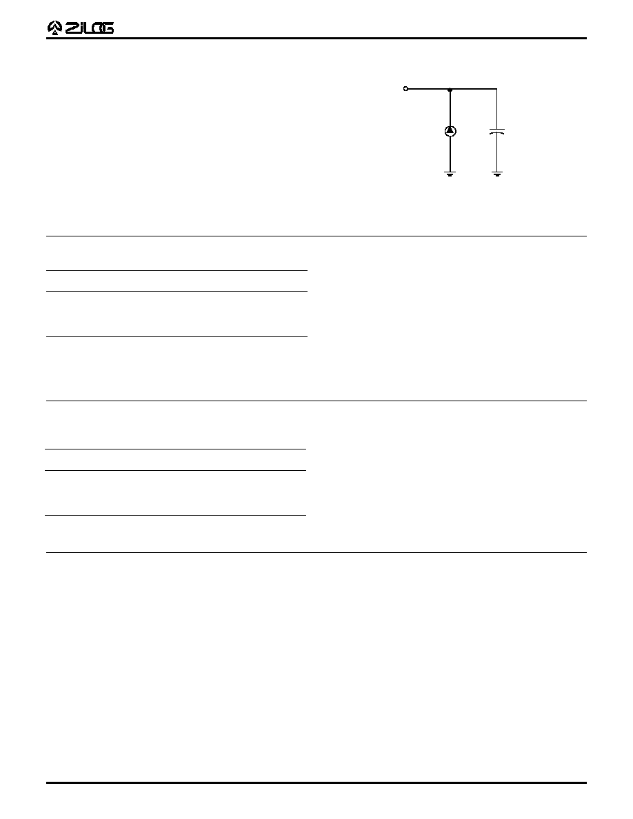
STANDARD TEST CONDITIONS
The characteristics listed below apply for standard test
conditions as noted. All voltages are referenced to Ground.
Positive current flows into the referenced pin (Figure 3).
From Output
Under Test
150 pF
I
Figure 3. Test Load Diagram
ABSOLUTE MAXIMUM RATINGS
Notes:
* Voltages on all pins with respect to Ground.
See Ordering Information.
Stresses greater than those listed under Absolute Maxi-
mum Ratings may cause permanent damage to the de-
vice. This is a stress rating only; operation of the device at
any condition above those indicated in the operational
sections of these specifications is not implied. Exposure to
absolute maximum rating conditions for extended periods
may affect device reliability.
Parameter
Min
Max
Input Capacitance
0
10 pF
Output Capacitance
0
20 pF
I/O Capacitance
0
25 pF
Sym
Parameter
Min
Max
Units
V
DD
Supply Voltage*
≠0.3
+7
V
T
STG
Storage Temp
≠65
∞
+150
∞
C
T
A
Oper Ambient Temp
C
V
CC
SPECIFICATION
V
CC
= 4.5V to 5.5V
When using the precision RC oscillator feature
f = 4.0 MHz
±
10% under the following conditions:
s
V
CC
= 5.0V
±
10%
s
Temp 0 to 40
∞
C
s
Application board capacitance: 2.0 pF max.
0.5 pF min.
CAPACITANCE
T
A
= GND = 0V, f = 1.0 MHz, unmeasured pins returned to Ground.

5
P R E L I M I N A R Y
Z86317
CMOS Z8
Æ
8-B
IT
MCU
DS96KEY1102
DC ELECTRICAL CHARACTERISTICS
T
A
= 0
∞
C to +40
∞
C
T y p i c a l
Symbol
Parameter
V
DD
Min
Max
@ 25
∞
C
Units
Conditions
V
CH
Clock Input High Voltage
5.5V
0.7 V
DD
V
DD
+ 0.3
3.0
V
Driven by External
Clock Generator
V
CL
Clock Input Low Voltage
5.5V
V
SS
≠ 0.3
0.2 V
DD
1.5
V
Driven by External
Clock Generator
V
IH
Input High Voltage
5.5V
0.7 V
DD
V
DD
+ 0.3
2.6
V
Schmitt-Triggered
V
IH
Input High Voltage
5.5V
0.7 V
DD
V
DD
+ 0.3
2.6
V
CMOS Input
V
IL
Input Low Voltage
5.5V
V
SS
≠ 0.3
0.2 V
DD
1.5
V
Schmitt-Triggered
V
IL
Input Low Voltage
5.5V
V
SS
≠ 0.3
0.2 V
DD
2.4
V
CMOS Input
V
OH
Output High Voltage
5.5V
V
DD
≠ 0.4
5.5
V
I
OH
= ≠2.0 mA
V
OL1
Output Low Voltage
5.5V
0.4
0.1
V
I
OL
= +4.0 mA
V
OL2
Output Low Voltage
5.5V
0.8
0.3
V
I
OL
= 10.0 mA,
6 Pin Max
V
LV
V
CC
Low Voltage Protection
2.5
3
2.7
V
@ 2 MHz Max
V
TP
Trip Point Voltage
5.5V
1.9
2.5
2.2
V
P24-P27
4.5V
1.5
2.1
1.8
V
I
IL
Input Leakage
5.5V
≠1.0
1.0
0.4
µ
A
V
IN
= OV, V
CC
I
OL
Output Leakage
5.5V
≠1.0
1.0
0.4
µ
A
V
IN
= OV, V
CC
I
DD
Supply Current
5.5V
3.0
1.44
mA
All Output and I/O Pins
Floating @ 1 MHz
5.5V
4.0
2.60
mA
All Output and I/O Pins
Floating @ 2 MHz
5.5V
6.0
4.28
mA
All Output and I/O Pins
Floating @ 4 MHz
I
DD1
Standby Current
5.5V
1.3
0.70
mA
HALT mode V
IN
= 0V,
V
CC
@ 1 MHz
5.5V
1.5
0.80
mA
HALT mode V
IN
= 0V,
V
CC
@ 2 MHz
5.5V
2.0
1.0
mA
HALT mode V
IN
= 0V,
V
CC
@ 4 MHz
I
PU
Pull-Up Current
4.5V
≠20
µ
A
V
IH
@ 3V
P00-02
5.5
≠85
µ
A
V
IH
@ 4V
P31, P33
I
PD
Pull-Down Current
4.5V
+20
µ
A
V
IL
@ 1V
P00-02
5.5
+95
µ
A
V
IL
@ 1V
P31, P33
I
PU
Pull-Up Current
4.5V
≠450
µ
A
V
IL
= 0V
P20, P22
5.5
≠85
µ
A
V
IL
= 0V
Notes:
The device is functional to V
LV
voltage. The minimum operational V
DD
is
determined by the value of the V
LV
voltage at ambient temperature. The
V
LV
voltage increases as the temperature decreases.
6
P R E L I M I N A R Y
Z86317
CMOS Z8
Æ
8-B
IT
MCU
DS96KEY1102
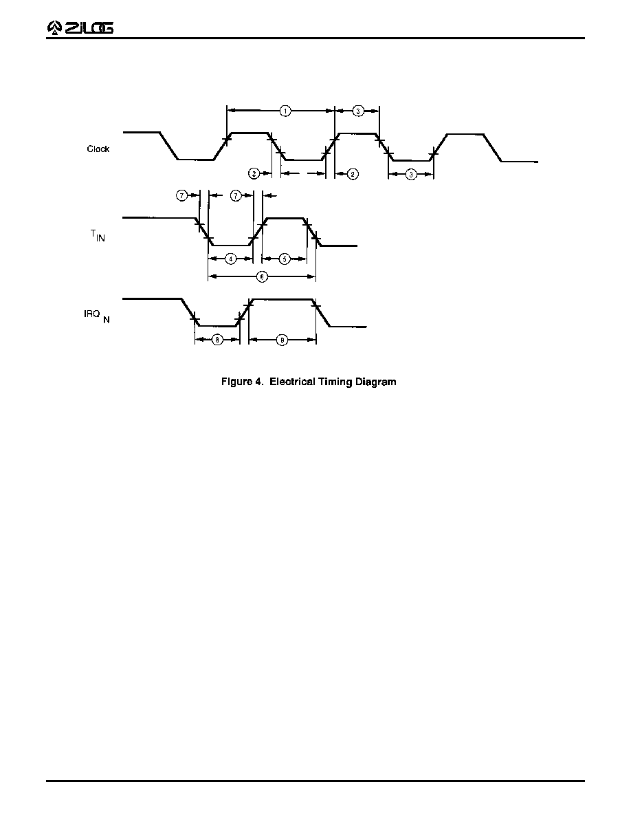
AC ELECTRICAL CHARACTERISTICS
Timing Diagrams
7
P R E L I M I N A R Y
Z86317
CMOS Z8
Æ
8-B
IT
MCU
DS96KEY1102
AC ELECTRICAL CHARACTERISTICS
T
A
= 0
∞
C to +40
∞
C
1 MHz
4 MHz
No Symbol
Parameter
V
DD
Min
Max
Min
Max
Units
Notes
1
TpC
Input Clock Period
5.5V
1,000
100,000
250
100,000
ns
[1]
2
TrC,TfC
Clock Input Rise
5.5V
25
25
ns
and Fall Times
3
TwC
Input Clock Width
5.5V
475
100
ns
[1]
4
TwTinL
Timer Input Low Width
5.5V
70
70
ns
[1]
5
TwTinH
Timer Input High Width
5.5V
2.5TpC
2.5TpC
[1]
6
TpTin
Timer Input Period
5.5V
4TpC
4TpC
[1]
7
TrTin,
Timer Input Rise
5.5V
100
100
ns
[1]
TtTin
and Fall Timer
8
TwIL
Int. Request Input
5.5V
70
70
ns
[1,2]
Low Time
9
TwIH
Int. Request Input
5.5V
2.5TpC
2.5TpC
[1,2]
High Time
10 Twdt
Watch-Dog Timer
5.5V
10
10
ms
[1]
Time Out Timer
11 T
POR
Power-On Reset Time
5.5V
2
2
ms
[1]
Notes:
[1] Timing Reference uses 0.9 V
DD
for a logic 1 and 0.1 V
DD
for a logic 0.
[2] Interrupt request through Port 3 (P33-P31)

8
P R E L I M I N A R Y
Z86317
CMOS Z8
Æ
8-B
IT
MCU
DS96KEY1102
© 1996 by Zilog, Inc. All rights reserved. No part of this document
may be copied or reproduced in any form or by any means
without the prior written consent of Zilog, Inc. The information in
this document is subject to change without notice. Devices sold
by Zilog, Inc. are covered by warranty and patent indemnification
provisions appearing in Zilog, Inc. Terms and Conditions of Sale
only. Zilog, Inc. makes no warranty, express, statutory, implied or
by description, regarding the information set forth herein or
regarding the freedom of the described devices from intellectual
property infringement. Zilog, Inc. makes no warranty of mer-
chantability or fitness for any purpose. Zilog, Inc. shall not be
responsible for any errors that may appear in this document.
Zilog, Inc. makes no commitment to update or keep current the
information contained in this document.
Zilog's products are not authorized for use as critical compo-
nents in life support devices or systems unless a specific written
agreement pertaining to such intended use is executed between
the customer and Zilog prior to use. Life support devices or
systems are those which are intended for surgical implantation
into the body, or which sustains life whose failure to perform,
when properly used in accordance with instructions for use
provided in the labeling, can be reasonably expected to result in
significant injury to the user.
Zilog, Inc. 210 East Hacienda Ave.
Campbell, CA 95008-6600
Telephone (408) 370-8000
FAX 408 370-8056
Internet: http://www.zilog.com