
DS96KEY0103 (8/96)
P R E L I M I N A R Y
1
1
P
RELIMINARY
P
RODUCT
S
PECIFICATION
Z86318
1
Z8
Æ
MCU 8-B
IT
M
ICROCONTROLLER
FEATURES
s
≠40
∞
C to +105
∞
C Operating Temperature Range
s
Low-Power Consumption: 33 mW (Typical)
s
ROM Mask Options:
≠
Permanent Watch-Dog Timer
≠
ROM Protect
≠
Low-Voltage Protection
≠
Pull-Up/Pull-Down I/O Pins
(Nibble Programmable)
≠
Feedback Resistor on the On-Chip Oscillator
s
On-Chip Oscillator (Crystal, Ceramic Resonator,
LC, or External Clock Drive)
s
Fast Instruction Pointer: 1.5
µ
s @ 4 MHz
s
ESD Protection Circuitry
GENERAL DESCRIPTION
The Z86318 is a member of the Z8
Æ
MCU family of CMOS
microcontrollers. This device offers on-board pull-up and
pull-down resistors (ROM mask-option programmable on a
nibble basis), a scalable trip-point buffer to accommodate
opto-transistor outputs, and high drive ports capable of up
to 20 mA current sinking per pin (3 pins maximum).
The Z86318 features I/O Ports (IOL = 20 mA at VOL =
0.8V, 3 pins max.) to provide increased current sinking ca-
pabilities. These devices also offer users a selection of
ROM mask options, which include a permanently enabled
Watch-Dog Timer that ensures operational reliability
across a broad range of application environments.
For applications requiring powerful I/O capabilities, the
Z86318 provides dedicated input and output lines that are
grouped into three ports. These ports can be configured by
means of ROM mask options (nibble-programmable) as
pull ups, pull downs, or neither. There are two basic ad-
dress spaces available. Program Memory, and 124 bytes
of general-purpose registers.
The Z86318 devices provide two on-chip 8-bit programma-
ble counter/timers with a large number of user-selectable
modes. Each counter/timer is driven by its own 6-bit pro-
grammable prescaler. The Z86318 counter/timers off-load
system real-time tasks such as counting/timing and in-
put/output data communications for increased system effi-
ciency.
Notes:
All Signals with a preceding front slash, "/", are ac-
tive Low, e.g.; B//W (WORD is active Low); /B/W (BYTE is
active Low, only).
Power connections follow conventional descriptions be-
low:
Device
ROM
(KB)
RAM*
(Bytes)
I/O
Lines
Voltage
Range
Z86318
124
14
21
0V to 6.0V
Note:
*General-Purpose
Connection
Circuit
Device
Power
VCC
VDD
Ground
GND
VSS
Z86318
Z8
Æ
MCU 8-Bit Microcontroller
2
P R E L I M I N A R Y
GENERAL DESCRIPTION
(Continued)
Figure 1. Z86318 Functional Block Diagram
Prg. Memory
3072 x 8-Bit (318)
2048 x 8-Bit (319)
Program
Counter
Port 3
Counter/
Timers (2)
Interrupt
Control
Port 2
I/O
(Bit Programmable)
ALU
FLAG
Register
Pointer
Register File
144 x 8-Bit
Machine
Timing & Inst.
Control
VSS
XTAL
VDD
Input
Port 0
I/O
Z86318
Z8
Æ
MCU 8-Bit Microcontroller
P R E L I M I N A R Y
3
1
PIN DESCRIPTIONS
ABSOLUTE MAXIMUM RATINGS
Stresses greater than those listed under Absolute Maxi-
mum Ratings may cause permanent damage to the de-
vice. This is a stress rating only; operation of the device at
any condition above those indicated in the operational sec-
tions of these specifications is not implied. Exposure to ab-
solute maximum rating conditions for extended periods
may affect device reliability.
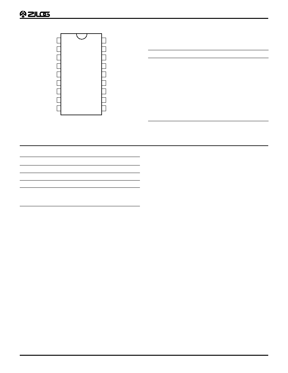
Figure 2. Z86318 18-Pin DIP/SOIC
Pin Configuration
1
2
9
3
4
5
6
7
8
18
17
16
15
14
13
12
11
10
P23
P22
P33
P21
P20
VSS
P02
P01
P00
P24
P25
P32
P26
P27
VDD
XTAL2
P31
Z86318
XTAL1
Table 1. Z86318 18 Pin DIP/SOIC Pin Identification
Pin #
Symbol
Function
Direction
1-4
P24-P27
Port 2, Pins 4, 5, 6, 7
In/Output
5
V
DD
Power Supply
Input
6
XTAL2
XTAL Osc. Clock
Output
7
XTAL1
XTAL Osc. Clock
Input
8
P31
Port 3, Pin 1
Input
9
P32
Port 3, Pin 2
Input
10
P33
Port 3, Pin 3
Input
11-13
P00-P02
Port 0, Pins 0, 1, 2
In/Output
14
V
SS
Ground
15-18
P20-P23
Port 2, Pins 0, 1, 2, 3
In/Output
Sym.
Parameter
Min.
Max.
Units
V
DD
Supply Voltage*
≠0.3
+7
V
T
STG
Storage Temp.
≠65
∞
+150
∞
C
T
A
Oper. Ambient Temp.
C
Note:
*Voltages on all pins with respect to Ground.
See Ordering Information.
Z86318
Z8
Æ
MCU 8-Bit Microcontroller
4
P R E L I M I N A R Y
STANDARD TEST CONDITIONS
The characteristics listed below apply for standard test
conditions as noted. All voltages are referenced to
Ground.Positive current flows into the referenced pin (Fig-
ure 3).
CAPACITANCE
TA = GND = 0V, f = 1.0 MHz, unmeasured pins returned to Ground.
V
CC
SPECIFICATION
V
CC
= 4.0V to 6.0V
Figure 3. Test Load Diagram
From Output
Under Test
150 pF
I
Parameter
Min.
Max.
Input Capacitance
0
10 pF
Output Capacitance
0
20 pF
I/O Capacitance
0
25 pF
Z86318
Z8
Æ
MCU 8-Bit Microcontroller
P R E L I M I N A R Y
5
1
DC ELECTRICAL CHARACTERISTICS
T
A
= 0
∞
C to +70
∞
C
Typical
Sym
Parameter
V
DD
Min
Max
@ 25
∞
C
Units
Conditions
Max Input Voltage
4.0V
12
V
V
IN
< 250
µ
A (Port Pins Only)
V
CH
Clock Input High
Voltage
4.0V
6.0V
0.7 V
DD
0.7 V
DD
V
DD
+ 0.3
V
DD
+ 0.3
2.0
3.0
V
V
Driven by External Clock Generator
V
CL
Clock Input Low
Voltage
4.0V
6.0V
V
SS
≠ 0.3
V
SS
≠ 0.3
0.2 V
DD
0.2 V
DD
0.8
1.5
V
V
Driven by External Clock Generator
V
IH
Input High Voltage
Schmitt-Triggered
4.0V
6.0V
0.7 V
DD
0.7 V
DD
V
DD
+ 0.3
V
DD
+ 0.3
1.6
2.6
V
V
V
IH
Input High Voltage
CMOS Input
4.0V
6.0V
0.7 V
DD
0.7 V
DD
V
DD
+ 0.3
V
DD
+ 0.3
1.4
2.6
V
V
V
IL
Input Low Voltage
Schmitt-Triggered
4.0V
6.0V
V
SS
≠ 0.3
V
SS
≠ 0.3
0.2 V
DD
0.2 V
DD
0.8
1.5
V
V
V
IL
Input Low Voltage
CMOS Input
4.0V
6.0V
V
SS
≠ 0.3
V
SS
≠ 0.3
0.2 V
DD
0.2 V
DD
1.3
2.4
V
V
V
OH
Output High
Voltage
4.0V
4.5V
V
DD
≠ 0.4
V
DD
≠ 0.4
2.8
4.4
V
V
I
OH
= ≠2.0 mA
V
OL1
Output Low Voltage
4.0V
6.0V
0.6
0.4
0.2
0.1
V
V
I
OL
= +4.0 mA
V
OL2
Output Low Voltage
4.0V
6.0V
1.5
0.8
0.8
0.3
V
V
I
OL
= 20.0 mA, 3 Pin Max
OL
= 10.0 mA, 6 Pin Max
V
LV
VCC Low-Voltage
Protection*
1.6
2.7
2.3
V
@ 2 MHz Max
V
TP
Trip-Point Voltage*
4.0V
4.5V
1.5
0.4 V
DD
2.1
1.8
V
V
P24-P27
5.5V
6.0V
1.9
2.1
2.5
2.7
2.2
2.4
V
V
V
OC
Input Open-Circuit
Voltage
4.5V
5.0V
0.95
1.05
1.15
1.25
1.04
1.15
V
V
No Off-Chip Resistance
5.5V
6.0V
1.15
1.25
1.39
1.49
1.27
1.37
V
V
I
IL
Input Leakage
3.0V
5.5V
6.0V
≠1.0
≠1.0
≠1.0
1.0
1.0
1.0
0.4
0.4
0.4
µ
A
µ
A
µ
A
V
IN
= 0V, VCC
I
OL
Output Leakage
4.0V
5.5V
6.0V
≠1.0
≠1.0
≠1.0
1.0
1.0
1.0
0.4
0.4
0.4
µ
A
µ
A
µ
A
V
IN
= 0V, VCC
Note:
*The Z86318 is functional to V
LV
voltage. The minimum operational V
DD
is determined by the value of the V
LV
voltage at
ambient temperature. The V
LV
voltage increases as temperature decreases.
Z86318
Z8
Æ
MCU 8-Bit Microcontroller
6
P R E L I M I N A R Y
DC ELECTRICAL CHARACTERISTICS (Continued)
T
A
= 0
∞
C to +70
∞
C
Typical
Sym.
Parameter
V
DD
Min.
Max.
@ 25
∞
C
Units Conditions
Notes
I
DD
Supply Current
4.0V
4.0V
4.0V
1.5
2.0
3.0
0.41
0.93
1.64
mA
mA
mA
@ 1 MHz
@ 2 MHz
@ 4 MHz
[1]
[1]
[1]
6.0V
6.0V
6.0V
3.0
4.0
6.0
1.44
2.60
4.28
mA
mA
mA
@ 1 MHz
@ 2 MHz
@ 4 MHz
[1]
[1]
[1]
I
DD1
Standby Current
4.0V
4.0V
4.0V
0.6
0.8
1.0
0.15
0.20
0.3
mA
mA
mA
HALT mode V
IN
= 0V, V
CC
@ 1 MHz
HALT mode V
IN
= 0V, V
CC
@ 2 MHz
HALT mode V
IN
= 0V, V
CC
@ 4 MHz
6.0V
6.0V
6.0V
1.3
1.5
2.0
0.70
0.80
1.0
mA
mA
mA
HALT mode V
IN
= 0V, V
CC
@ 1 MHz
HALT mode V
IN
= 0V, V
CC
@ 2 MHz
HALT mode V
IN
= 0V, V
CC
@ 4 MHz
I
DD2
Standby Current
6.0V
10
1.5
mA
STOP mode V
IN
= 0V, V
CC
I
PU
Pull-Up Current (100K)
Port P00≠P02;
Port P22, P23;
Port P31≠P33
4.5V
6.0V
-20
105
µ
A
V
IH
@ 1V
V
IH
@ 1V
I
PD
Pull-Down Current (100K)
Port P00≠P02;
Port P22, P23;
Port P31≠P33
4.5V
6.0V
20
114
µ
A
V
IL
@ 3V
V
IL
@ 4V
I
PU
Pull-Up Current (10K)
Port P20, P21
4.5V
6.0V
208
870
µ
A
V
IH
@ 0V
V
IH
@ 0V
I
PD
Pull-Down Current (10K)
Port P20, P21
4.5V
6.0V
170
870
µ
A
V
IH
@ 3V
V
IH
@ 3V
Note: [1] All outputs unloaded, I/O pins floating, inputs at rail.
Z86318
Z8
Æ
MCU 8-Bit Microcontroller
P R E L I M I N A R Y
7
1
AC ELECTRICAL CHARACTERISTICS
Timing Diagrams
Figure 4. Electrical Timing Diagram
1
3
4
8
2
2
3
T
IRQ
IN
N
6
5
7
7
9
Clock
Z86318
Z8
Æ
MCU 8-Bit Microcontroller
8
P R E L I M I N A R Y
AC ELECTRICAL CHARACTERISTICS
(V
DD
= 4V to 6V
±
10%, T
A
= 0
∞
C to +70
∞
C, unless otherwise specified)
T
A
= 0
∞
C to +70
∞
C
1 MHz
4 MHz
No.
Symbol
Parameter
V
DD
Min.
Max.
Min.
Max.
Units
Notes
1
TpC
Input Clock Period
6.0V
1,000
100,000
250
100,000
ns
[1]
2
TrC,TfC
Clock Input Rise
and Fall Times
6.0V
25
25
ns
3
TwC
Input Clock Width
6.0V
475
100
ns
[1]
4
TwTinL
Timer Input Low Width
6.0V
70
70
ns
[1]
5
TwTinH
Timer Input High Width
6.0V
2.5TpC
2.5TpC
[1]
6
TpTin
Timer Input Period
6.0V
4TpC
4TpC
[1]
7
TrTin,
TtTin
Timer Input Rise
and Fall Timer
6.0V
100
100
ns
[1]
8
TwIL
Int. Request Input
Low Time
6.0V
70
70
ns
[1,2]
9
TwIH
Int. Request Input
High Time
6.0V
2.5TpC
2.5TpC
[1,2]
10
Twdt
Watch-Dog Timer
6.0V
24
24
ms
11
T
POR
Power-On Reset Time
6.0V
6
6
ms
[1]
Notes:
1. Timing Reference uses 0.9 VDD for a logic 1 and 0.1 VDD for a logic 0.
2. Interrupt request through Port 3 (P33-P31).
Z86318
Z8
Æ
MCU 8-Bit Microcontroller
P R E L I M I N A R Y
9
1
PIN FUNCTIONS
XTAL1, XTAL2. Crystal in, crystal out (time-based input
and output, respectively). These pins connect a parallel-
resonant crystal, LC, or an external single-phase clock (4
MHz Max.) to the on-chip clock oscillator and buffer. Note:
XTAL1 has a pull-down resistor.
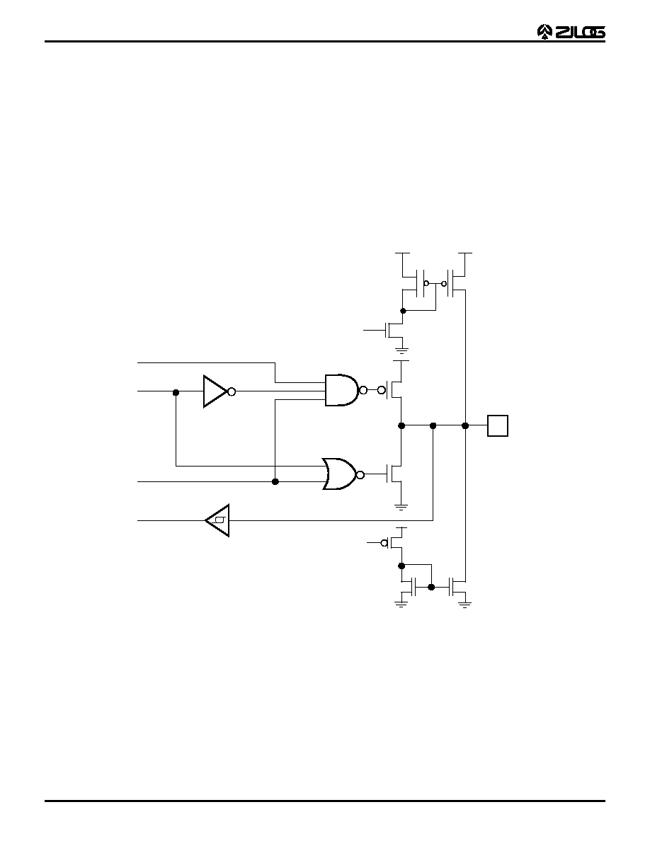
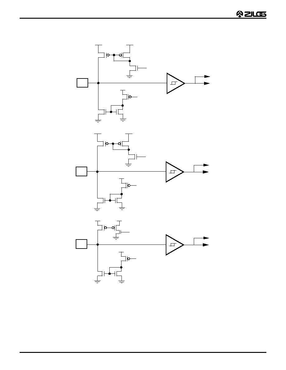
Port 0 (P02-P00). Port 0 is a 3-bit, I/O programmable, bi-
directional, CMOS-compatible I/O port. These three I/O
lines can be configured under software control to be input
or output (see Figure 5). When Port 0 is configured as an
input port, all lines have the capability to be globally con-
figured (ROM mask option) for a 100K pull-down or pull-up
resistor. The pull-up/pull-down resistor can be disabled as
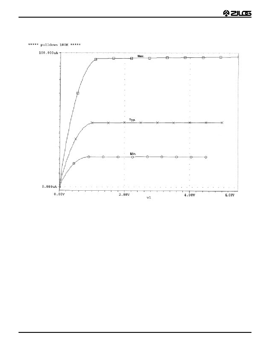
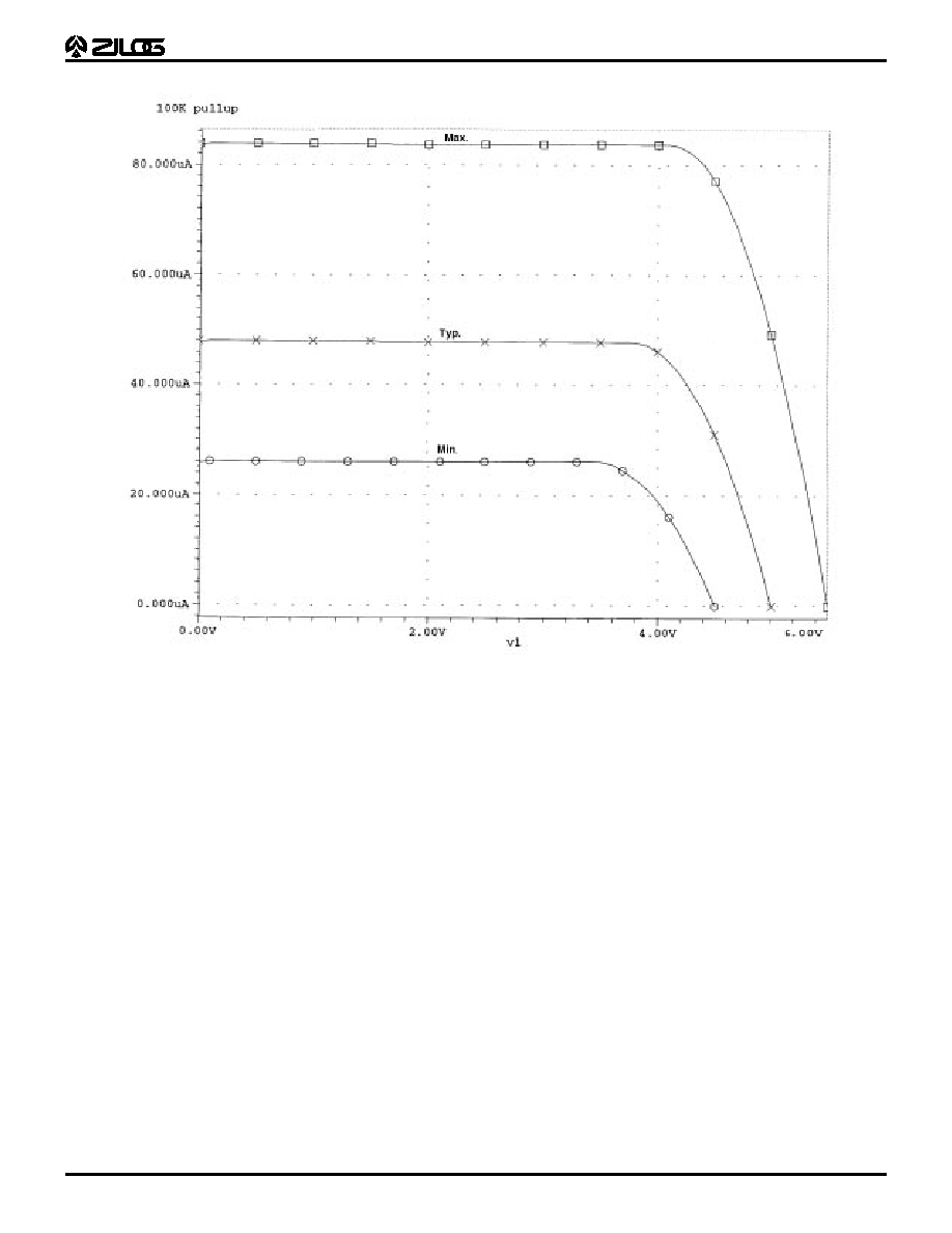
well. (No current is drawn if disabled.) Graphs showing
current versus pin voltage are shown in Figures 6 and 7.
Figure 5. Port 0 Configuration
/OEN
Out
In
Pad
Pull-Down
Enable
Pull-Up
Enable
Z86318
Z8
Æ
MCU 8-Bit Microcontroller
10
P R E L I M I N A R Y
PIN FUNCTIONS (Continued)
Figure 6. Typical Current Versus Pin Voltage Values
Z86318
Z8
Æ
MCU 8-Bit Microcontroller
P R E L I M I N A R Y
11
1
Figure 7. Typical Current Versus Pin Voltage Values
Z86318
Z8
Æ
MCU 8-Bit Microcontroller
12
P R E L I M I N A R Y
PIN FUNCTIONS (Continued)
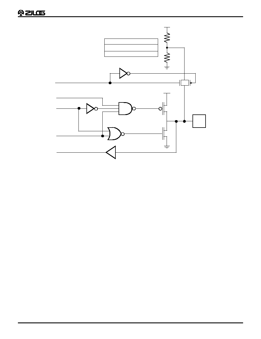
Port 2 (P27-P20). Port 2 is an 8-bit, bit-programmable, bi-
directional, CMOS-compatible I/O port. P23-P20 can be
configured under software control to be input or output, in-
dependently. Note: Bits D3 and D4 of POIM register must
be set to 0. Bits programmed as outputs may be globally
programmed as either push-pull or open-drain via bit D0,
P3M register. P20 and P21 can be configured with a ROM
mask option for 10 Kohm pull-up/pull-down, or none. P22
and P23 can be configured with a ROM mask option for
100 Kohm pull-up/pull-down, or none (Figure 8). No cur-
rent is drawn if pull-up/pull-down is disabled. Note: P23-20
are configured for pull-up/pull-down/none globally.
P24-P27 can be configured as a voltage divider. The volt-
age divider consists of an internal 25K pull-up resistor (Fig-
ure 9), and a 7.5K pull-down resistor. The zero trip-point in-
put levels on P24-P27 are adjusted for connection to the
emitters of opto-transistors and switch at a voltage level of
0.4 VDD. All four of the voltage dividers are globally con-
figured as enabled or disabled.
Figure 8. Port 2 P20-P23 Configuration
/OEN
Out
In
Pad
Pull-Down
Enable
Pull-Up
Enable
Note: P20, P21: 10K Pull-Up/Down or none.
P22, P23: 100K Pull-Up/Down or none.
P23-20 are globally selected for Pull-Up/Down or none.
/Open-Drain
Z86318
Z8
Æ
MCU 8-Bit Microcontroller
P R E L I M I N A R Y
13
1
Port 3 (P33, P32, P31). Port 3 is a 3-bit, CMOS-compati-
ble port with three fixed input lines (P33≠P31). These three
lines can also be used as the interrupt sources IRQ2,
IRQ1, and IRQ0. P31 can also be configured as a timer in-
put.
All three lines can be configured globally by means of ma
ROM mask option for a 100 Kohm pull-up or pull-down re-
sistor (Figure 10), or no pull-up/pull-down. No current is
drawn if pull-up/pull-down is disabled.
Figure 9. Port 2 P27-P24 Configuration
/OE
Out
In
Pad
/Open-Drain
0.4 VDD
Trip Point Buffer
7.5K
25K
Resistance Tolerance (0 - +40
∞
C)
Min.
Max.
Typ.
Pull-Down
Pull-Up
5.2K
7.5K
8.9K
18K
25K
30K
Divenb
Z86318
Z8
Æ
MCU 8-Bit Microcontroller
14
P R E L I M I N A R Y
PIN FUNCTIONS (Continued)
Figure 10. Port 3 P31-P33 Configuration
P31
Pad
P33
IRQ2, TIN
Data Latch
Data Latch
IRQ1
Pad
Pull-Up
Enable
Pull-Down
/Enable
Pull-Up
Enable
Pull-Down
/Enable
P32
Pad
Data Latch
Pull-Up
Enable
Pull-Down
/Enable
Z86318
Z8
Æ
MCU 8-Bit Microcontroller
P R E L I M I N A R Y
15
1
The Z86318 MCU incorporates the following special fea-
tures to enhance the Z8
Æ
architectural core for use in
mouse and trackball applications.
Reset. The Z86318 is reset in one of the following condi-
tions: 1) Power-On Reset (POR), 2) Watch-Dog Timer
(WDT) Mode, 3) Stop-Mode Recovery source, and 4) Low-
Voltage Recovery. Other sources of Reset, ports are con-
figured in an input mode, asynchronous of the clock. How-
ever, a clock is required to generate the internal reset that
resets the internal registers.
Auto POR circuitry is built into the Z86318, eliminating the
need for an external reset circuit to reset on power-on.
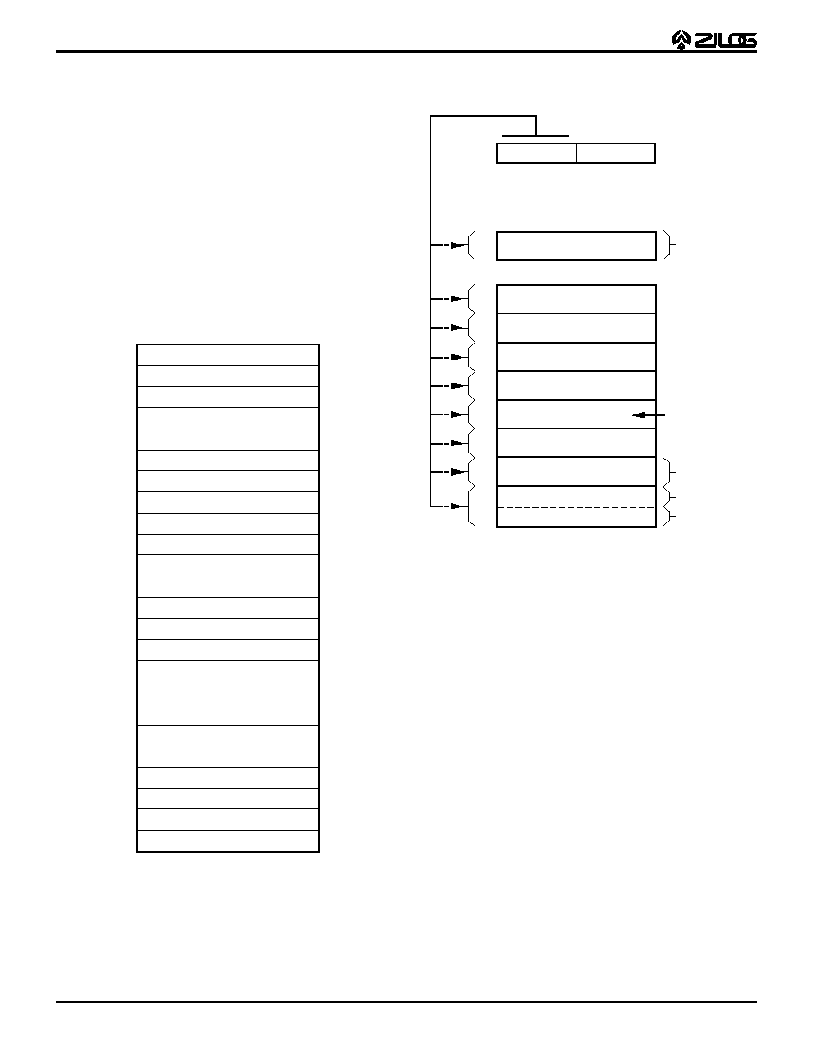
Program Memory. The Z86318 device can address up to
3 KB of internal program memory (Figure 11). The first 12
bytes of Program Memory are reserved for the interrupt
vectors. These locations contain four 16-bit vectors that
correspond to the four available interrupts. Bytes 0-3064
are programmed on-chip by means of a ROM mask option.
Table 2. Z86318 Control Registers
Reset Values
Addr.Reg.
D7 D6 D5 D4 D3 D2 D1 D0 Comments
F1
TMR
0
0
0
0
0
0
0
0
F2
T1
U
U
U
U
U
U
U
U
F3
PRE1 U
U
U
U
U
U
0
0
F4
T0
U
U
U
U
U
U
U
U
F5
PRE0 U
U
U
U
U
U
U
0
F6*
P2M
1
1
1
1
1
1
1
1
Inputs after
reset
F7*
P3M
U
U
U
U
U
U
1
0
F8*
P01M U
U
U
0
U
U
0
1
F9
IPR
U
U
U
U
U
U
U
U
FA
IRQ
U
U
0
0
0
0
0
0
FB
IMR
0
U
U
U
U
U
U
U
FC
FLAGS U
U
U
U
U
U
U
U
FD
RP
U
U
U
U
U
U
U
U
FF
SPL
U
U
U
U
U
U
U
U
Notes: *
A reset after a Low on P27 to exit STOP mode may
affect device reliability.
Figure 11. Program Memory Map
On-Chip
ROM
Location of
First Byte of
Instruction
Executed
After RESET
Interrupt
Vector
(Lower Byte)
Interrupt
Vector
(Upper Byte)
IRQ5
IRQ4
IRQ4
Reserved
Reserved
IRQ2
IRQ2
IRQ1
IRQ1
Reserved
Reserved
IRQ5
3064
12
11
10
9
8
7
6
5
4
3
2
1
0
Z86318
Z8
Æ
MCU 8-Bit Microcontroller
16
P R E L I M I N A R Y
FUNCTIONAL DESCRIPTION
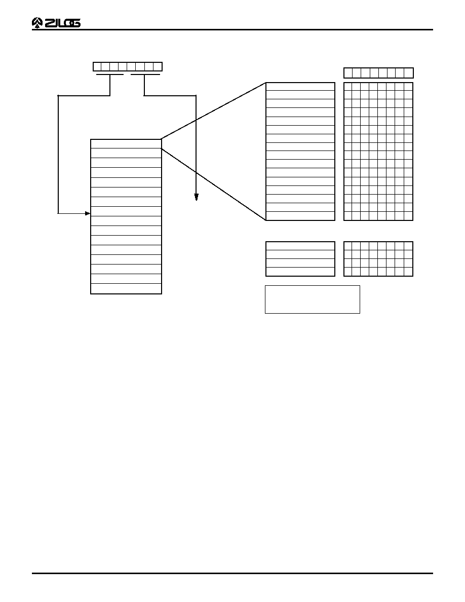
Register File. The Register File consists of three I/O port
registers, 124 general-purpose registers, and 15 control
and status registers, R0-R3, R4-R127 and R241-R255, re-
spectively (see Figure 12). The Z86318 instructions can
access registers directly or indirectly via an 8-bit address
field. This allows short, 4-bit register addressing using the
Register Pointer.
In the 4-bit mode, the register file is divided into eight
working register groups, each occupying 16 continuous lo-
cations. The Register Pointer addresses the starting loca-
tion of the active working-register group (Figures 13 and
14).
Figure 12. Register File
Stack Pointer (Bits 7-0)
R255
General-Purpose
Register Pointer
Program Control Flags
Interrupt Mask Register
Interrupt Request Register
Interrupt Priority Register
Ports 0-1 Mode
Port 3 Mode
Port 2 Mode
T0 Prescaler
Timer/Counter0
T1 Prescaler
Timer/Counter1
Timer Mode
R254
R253
R252
R251
R250
R249
R248
R247
R246
R245
R244
R243
R242
R241
SPL
RP
FLAGS
IMR
IRQ
IPR
P01M
P3M
P2M
PRE0
T0
PRE1
T1
TMR
LOCATION
IDENTIFIERS
GPR
General-Purpose
Registers
Port 3
Port 2
Reserved
Port 0
R127
R3
R2
R1
R0
P3
P2
P0
R4
R128
Not Implemented
Figure 13. Register Pointer
The upper nibble of the register file address
provided by the register pointer specifies
the active working-register group.
r7
r6
r5
r4
R253
(Register Pointer)
I/O Ports
Specified Working
Register Group
The lower nibble
of the register
file address
provided by the
instruction points
to the specified
register.
r3
r2
r1
r0
Register Group 1
Register Group 0
R15 to R0
Register Group F
R15 to R4
R3 to R0
R15 to R0
FF
F0
0F
00
1F
10
2F
20
3F
30
4F
40
5F
50
6F
60
7F
70
Z86318
Z8
Æ
MCU 8-Bit Microcontroller
P R E L I M I N A R Y
17
1
ROM Protect. A ROM Protect feature prevents "dumping"
of the ROM contents without inhibiting execution of LDC,
LDCI, LDE, and LDEI instructions. This feature is mask-
programmable.
Stack Pointer. The Z86318 features an 8-bit Stack Point-
er (R255) used for the internal stack that resides within the
124 general-purpose registers.
Counter/Timer. There are two 8-bit programmable
counter/timers (T0 and T1), each driven by its own 6-bit
programmable prescaler. The T1 prescaler can be driven
by internal or external clock sources, however, the T0 can
be driven by the internal clock source only (see Figure 15).
The 6-bit prescalers can divide the input frequency of the
clock source by any integer number from 1 to 64. Each
prescaler drives its counter, which decrements the value
(1 to 256) that has been loaded into the counter. When
both counter and prescaler reach the end of count, a timer
interrupt request IRQ4 (T0) or IRQ5 (T1) is generated.
Figure 14. Register File Architecture
7
6
5
4
3
2
1
0
Working Register
Group Pointer
Bits 0-3 must be 0
% FF
% FO
% 7F
% 0F
% 00
Z8 Register File
REGISTER POINTER
% FF
% FE
% FD
% FC
% FB
% FA
% F9
% F8
% F7
% F6
% F5
% F4
% F3
% F2
% F1
% F0
SPL
GPR
RP
FLAGS
IMR
IRQ
IPR
P01M
P3M
P2M
U
U
0
U
0
0
U
0
0
1
U
U
0
U
U
0
U
1
0
1
U
U
0
U
U
0
U
0
0
1
U
U
0
U
U
0
U
0
0
1
U
U
0
U
U
0
U
1
0
1
U
U
0
U
U
0
U
1
0
1
U
U
0
U
U
0
U
0
0
1
U
U
0
U
U
0
U
1
0
1
REGISTER
Z8
Æ
STANDARD CONTROL REGISTERS
RESET CONDITION
D7 D6 D5 D4 D3 D2 D1 D0
*
*
PRE0
U
U
U
U
U
U
U
U
U
U
U
U
U
U
U
U
U
U
U
U
U
U
U
U
U
U
U
U
U
U
U
U
0
0
0
0
0
0
0
0
T0
PRE1
T1
TMR
Reserved
% EO
U = Unknown
* Will not be reset with a Stop-Mode Recovery
All addresses are in Hexadecimal
Notes:
0
0
0
0
U
U
U
U
U
U
U
U
U
U
U
U
U
U
U
U
U
U
U
U
REGISTER
RESET CONDITION
% (0) 03
P3
% (0) 02
P2
% (0) 01
Reserved
% (0) 00
P0
*
*
Z86318
Z8
Æ
MCU 8-Bit Microcontroller
18
P R E L I M I N A R Y
FUNCTIONAL DESCRIPTION (Continued)
The counter can be programmed to start, stop, restart to
continue, or restart from the initial value. The counters can
also be programmed to stop upon reaching zero (single
pass mode) or to automatically reload the initial value and
continue counting (modulo-n continuous mode).
The counters, but not the prescalers, may be read at any
time without disturbing their value or count mode. The
clock source for T1 is user-definable and can be either the
internal microprocessor clock divided by four, or an exter-
nal signal input via Port 3. The Timer Mode register config-
ures the external timer input (P31) as an external clock, a
trigger input that is retriggerable or not retriggerable, or as
a gate input for the internal clock.
Figure 15. Counter/Timers Block Diagram
PRE0
Initial Value
Register
T0
Initial Value
Register
T0
Current Value
Register
6-Bit
Down
Counter
8-Bit
Down
Counter
˜
4
OSC
6-Bit
Down
Counter
8-Bit
Down
Counter
PRE1
Initial Value
Register
T1
Initial Value
Register
T1
Current Value
Register
Clock
Logic
IRQ4
IRQ5
Internal Data Bus
Write
Write
Read
Internal Clock
Gated Clock
Triggered Clock
Write
Write
Read
Internal Data Bus
External Clock
Internal
Clock
˜
4
T P31
IN
Z86318
Z8
Æ
MCU 8-Bit Microcontroller
P R E L I M I N A R Y
19
1
Interrupts. The Z86318 features four interrupts from four
different sources. These interrupts are maskable and pri-
oritized (Figure 16). The four sources are divided as fol-
lows: the falling edge of P31, P33, and the two counter/tim-
ers. The Interrupt Mask Register globally or individually
enables or disables the four interrupt requests (Table 4).
When more than one interrupt is pending, priorities are re-
solved by a programmable priority encoder that is con-
trolled by the Interrupt Priority register. All Z86318 inter-
rupts are vectored through locations in program memory.
When an interrupt machine cycle is activated, an interrupt
request is granted. This disables all subsequent interrupts,
saves the Program Counter and Status Flags, and then
branches to the program memory vector location reserved
for that interrupt. This memory location and the next byte
contain the 16-bit starting address of the Interrupt Service
Routine for that particular interrupt request.
To accommodate polled interrupt systems, interrupt inputs
are masked and the Interrupt Request Register is polled to
determine which of the interrupt requests needs service.
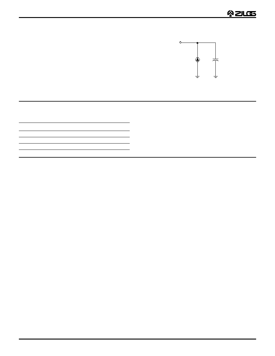
Clock. The Z86318 on-chip oscillator has a parallel-reso-
nant amplifier for connection to a crystal, ceramic resona-
tor, or any suitable external clock source (XTAL1 = Input,
XTAL2 = Output). The crystal should be AT cut, 4 MHz
max, with a series resistance (RS) less than or equal to
100 Ohms.
The crystal should be connected across XTAL1 and
XTAL2 using the recommended capacitors (capacitance is
between 10 pF to 250 pF and is specified by the crystal
manufacturer, ceramic resonator and PCB layout) from
each pin to ground (see Figure 17).
Table 3. Interrupt Types, Sources, and Vectors
Source
Name
Vector
Location Comments
P33
IRQ1
2,3
External
(F)Edge
P31
IRQ2 4,5
External
(F)Edge
T0
IRQ4
8,9
Internal
T1
IRQ5 10,11
Internal
Notes:
F = Falling edge triggered
R = Rising edge triggered
Figure 16. Interrupt Block Diagram
IRQ
IMR
IPR
Priority
Logic
6
Vector Select
Global
Interrupt
Enable
Interrupt
Request
IRQ0 - IRQ5
Z86318
Z8
Æ
MCU 8-Bit Microcontroller
20
P R E L I M I N A R Y
FUNCTIONAL DESCRIPTION (Continued)
HALT Mode. This instruction turns off the internal CPU
clock but not the on-chip oscillation circuit. The
counter/timers and external interrupts IRQ1 and IRQ2 re-
main active. The device can be recovered by interrupts, ei-
ther externally or internally generated. An interrupt request
must be executed (enabled) to exit HALT mode. After the
interrupt service routine, the program continues from the
instruction after the HALT. The HALT mode may also be
exited via POR/RESET activation or a WDT time-out. In
this case, the program execution begins at location
000CH. The WDH instruction is used to enable the Watch-
Dog Timer in HALT mode.
STOP Mode. This instruction turns off the internal clock
and reduces the standby current. The STOP mode can be
released by the following methods: 1) Power-On Reset
(POR) and 2) P27 is configured as an input line when the
device executes the STOP instruction. A low input condi-
tion on P27 that meets a minimum pulse width (TWSM) re-
leases the STOP mode. Note: WDT is disabled in STOP
mode.
Upon reset, program execution begins at location 000C
(hex). However, when P27 is used to release the STOP
mode, the I/O port mode registers are not reconfigured to
their default power-on conditions. This prevents any I/O,
configured as an output when the STOP instruction was
executed, from glitching to an unknown state. To use the
P27 release approach with STOP mode, use the following
instruction:
LDP2M, #1XXX XXXXB(X = user's choice)
NOP
STOP
In order to enter STOP (or HALT) mode, it is necessary to
first flush the instruction pipeline to avoid suspending exe-
cution in mid-instruction. To do this, the user must execute
a NOP (opcode=FFH) immediately before the appropriate
sleep instruction, such as the following:
In STOP or HALT mode, the value of each output line prior
to the HALT or STOP instruction is retained during execu-
tion.
Figure 17. Oscillator Configuration
XTAL1
XTAL2
C1
C2
C1
C2
XTAL1
XTAL2
Ceramic
Resonator
or Crystal
L
LC Clock
XTAL1
XTAL2
External Clock
FF
NOP
; clear the pipeline
6F
STOP
; enter the STOP
mode
or
FF
NOP
; clear the pipeline
7F
HALT
; enter the HALT
mode
Z86318
Z8
Æ
MCU 8-Bit Microcontroller
P R E L I M I N A R Y
21
1
Watch-Dog Timer (WDT). The WDT is initially enabled by
executing the WDT instruction and it is refreshed by sub-
sequent WDT instruction executions. Note: Once the WDT
has been enabled, it cannot be disabled. The time-out pe-
riod of the WDT is 24 ms. The WDT instruction affects the
Zero (Z), Sign (S), and Overflow (V) flags. The WDT can
be permanently enabled (ROM mask option) upon MCU
power-up.
Opcode WDT (5FH). Execution of WDT clears the WDT
counter. This must be done at least every 24 ms, other-
wise, the WDT times out and generates a reset. This gen-
erated reset is the same as a power-on reset of 6.0 ms,
plus 18 clock cycles.
Low-Voltage Protection (V
LV
). The device will function
normally between 6.0V and 4.0V under all specified condi-
tions. Below 4.0V, the device is still internally functional un-
til the Low Voltage trip point (V
LV
) is reached; however, it
is not guaranteed to meet all AC and DC Characteristics.
When the supply voltage drops below V
LV
, an automatic
hardware reset occurs, re-initializing the Z86318. The
Low-Voltage Protection feature may be selected as a
ROM mask option.
The actual V
LV
is a function of temperature, operating fre-
quency and process parameters. A typical example of the
V
LV
trip-point function at ambient temperature for a fre-
quency of 4 MHz is illustrated in Figure 18.
Figure 18. Typical Z86318 V
LV
Versus Temperature
Vcc
(Volts)
2.80
2.75
2.70
2.65
2.60
2.55
2.50
≠5
0
5
10
15
20
25
30
35
40
45
Temperature (
∞
C)
L
LV
(Typical)
Z86318
Z8
Æ
MCU 8-Bit Microcontroller
22
P R E L I M I N A R Y
Z8 CONTROL REGISTERS
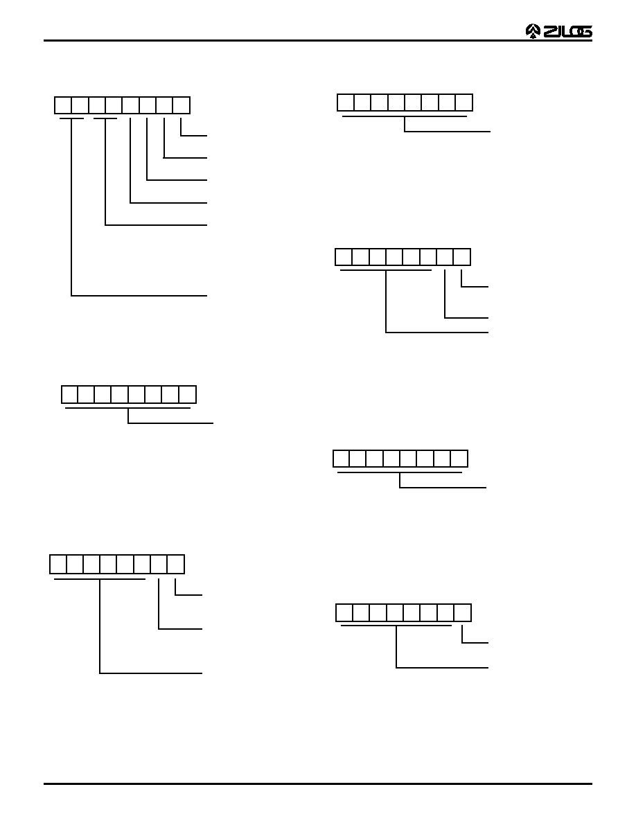
Figure 19. Timer Mode Register (F1
H
:Read/Write)
Figure 20. Counter Timer 1 Register (F2
H
: Read/Write)
Figure 21. Prescaler 1 Register (F3
H
:Write Only)
D7 D6
D5
D4
D3 D2
D1
D0
0 Disable T0 Count
1 Enable T0 Count
0 No Function
1 Load T0
0 No Function
1 Load T1
0 Disable T1 Count
1 Enable T1 Count
TIN Modes
00 External Clock Input
01 Gate Input
10 Trigger Input
(Non-retriggerable)
11 Trigger Input
(Retriggerable)
Reserved (Must be 0)
R241 TMR
D7
D6
D5
D4
D3
D2
D1
D0
T1 Initial Value
(When Written)
(Range 1-256 Decimal
01-00 HEX)
T1 Current Value
(When READ)
R242 T1
D7 D6 D5 D4 D3 D2 D1 D0
Count Mode
0 T1 Single Pass
1 T1 Modulo
Clock Source
1 T1 Internal
0 T1 External Timing Input
(TIN) Mode
Prescaler Modulo
(Range: 1-64 Decimal
01-00 HEX)
R243 PRE1
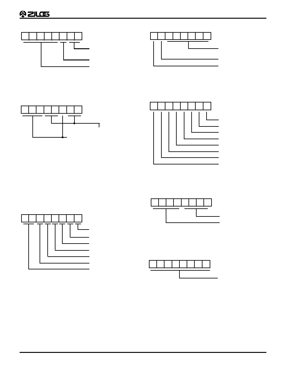
Figure 22. Counter Timer 0 Register (F4
H
: Read/Write)
Figure 23. Prescaler 0 Register (F5
H
: Write Only)
Figure 24. Port 2 Mode Register (F6
H
: Write Only)
Figure 25. Port 3 Mode Register (F7
H
: Write Only)
D7
D6
D5
D4
D3
D2
D1
D0
T0 Initial Value
(When Written)
(Range: 1-256 Decimal
01-00 HEX)
T0 Current Value
(When READ)
R244 T0
0 T0 Single Pass
1 T0 Modulo N
D7
D6
D5 D4
D3
D2
D1
D0
Count Mode
Reserved (Must be 0)
Prescaler Modulo
(Range: 1-64 Decimal
01-00 HEX)
R245 PRE0
D7
D6
D5
D4
D3
D2
D1
D0
P27- P20 I/O Definition
0 Defines Bit as OUTPUT
1 Defines Bit as INPUT
R246 P2M
0 Port 2 Open-Drain
1 Port 2 Push-Pull
D7 D6
D5
D4
D3 D2
D1
D0
Reserved (Must be 0)
R247 P3M
Z86318
Z8
Æ
MCU 8-Bit Microcontroller
P R E L I M I N A R Y
23
1
Figure 26. Port 0 and 1 Mode Register
(F8
H
: Write Only)
Figure 27. Interrupt Priority Register (F9
H
: Write Only)
Figure 28. Interrupt Request Register
(FA
H
: Read/Write)
D7
D6
D5
D4
D3
D2
D1
D0
R248 P01M
P00-P03 Mode
00 Output
01 Input
Reserved (Must be 0)
Reserved (Must be 0)
D7 D6
D5
D4
D3
D2
D1
D0
Reserved
(Must be 0.)
R249 IPR
0000
0001
0010
0011
0100
0101
0110
0111
1000
1001
1010
1011
1100
1101
1110
1111
Reserved
IRQ1>4>5>2
Reserved
IRQ4>1>5>2
IRQ5>2>1>4
IRQ5>1>4>2
IRQ5>2>4>1
IRQ5>4>1>2
IRQ2>1>4>5
IRQ1>4>2>5
IRQ2>4>1>5
IRQ4>1>2>5
IRQ2>5>1>4
Reserved
IRQ2>5>4>1
Reserved
D7 D6
D5
D4
D3 D2
D1
D0
R250 IRQ
IRQ2 = P31 Input
IRQ1 = P33 Input
IRQ4 = T0
IRQ5 = T1
Reserved (Must be 0)
Reserved (Must be 0)
Reserved (Must be 0)
Figure 29. Interrupt Mask Register (FB
H
: Read/Write)
Figure 30. Flag Register (FC
H
: Read/Write)
Figure 31. Register Pointer (FD
H
: Read/Write)
Figure 32. Stack Pointer (FFH: Read/Write)
D7
D6
D5
D4
D3
D2
D1
D0
1 Enables IRQ5-IRQ0
(D0 = IRQ0)
Reserved (Must be 0)
1=Global Interrupt Enable
0=Global Interrupt Disable
R251 IMR
D7
D6
D5
D4
D3
D2
D1
D0
User Flag F1
User Flag F2
Half Carry Flag
Decimal Adjust Flag
Overflow Flag
Sign Flag
Zero Flag
Carry Flag
R252 Flags
D7
D6
D5
D4
D3
D2
D1
D0
Reserved (Must be 0)
Working Register Pointer
R253 RP
D7
D6
D5
D4
D3
D2
D1
D0
Stack Pointer Lower
Byte (SP0-SP7)
R255 SPL
Z86318
Z8
Æ
MCU 8-Bit Microcontroller
24
P R E L I M I N A R Y
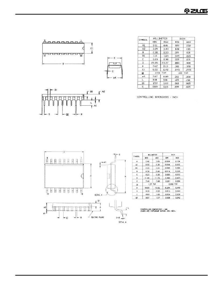
PACKAGE INFORMATION
Figure 33. 18-Pin DIP Package Diagram
Figure 34. 18-Pin SOIC Package Diagram
Z86318
Z8
Æ
MCU 8-Bit Microcontroller
P R E L I M I N A R Y
25
1
ORDERING INFORMATION
For fast results, contact your local Zilog sales offices for
assistance in ordering the part desired.
Codes
Preferred Package
P = DIP
Longer Lead Time
S = SOIC
Temperature
S = 0
∞
C to +70
∞
C
Speed
04 = 4 MHz
Environmental
C = Plastic Standard
Z86318
18-Pin DIP
18-Pin SOIC
Z8631804PSC
Z8631804SSC
Z8631804PEC
Z8631804SEC
Example:
Z 86318 04 P S C
is a Z86318, 4 MHz, DIP
, 0
∞
C to +70
∞
C, Plastic Standar
d Flow
Environmental Flow
Temperature
Package
Speed
Product Number

Z86318
Z8
Æ
MCU 8-Bit Microcontroller
26
P R E L I M I N A R Y