Document Outline
- Preliminary Product Specification
- FEATURES
- GENERAL DESCRIPTION
- pin descriptions
- Figure�2.� 18-Pin DIP/SOIC Pin Configuration
- Table�1.� 18-Pin DIP/SOIC Pin Identification
- 1-4
- P24-P27
- Port 2, Pins 4,5,6,7
- In/Output
- 5
- VDD
- Power Supply
- Power
- 6
- RCIN
- RC Oscillator
- Input
- 7
- AGND
- Analog Ground
- Ground
- 8
- P31
- Port 3, Pin 1
- Input
- 9
- GND
- Ground
- Input
- 10
- P33
- Port 3, Pin 3,
- Input
- 11-13
- P00-P02
- Port 0, Pins 0,1,2
- In/Output
- 14
- GND
- Ground
- Ground
- 15-18
- P20-P23
- Port 2, Pins 0,1,2,3
- In/Output
- PIN functions
- standard test conditions
- DC ELECTRICAL CHARACTERISTICS
- 4.5V ≥ VDD ≤ 5.5V
- VIH
- Rising Input
- Schmitt-Triggered
- 2.3
- 3.2
- V
- Note 1
- VIL
- Falling Input
- Schmitt-Triggered
- 1.3
- 2.2
- V
- Note 1
- VIL
- Input Low Voltage CMOS Input
- V
- VOH
- Output High Voltage
- VDD Ö 0.4
- V
- IOH = Ö2.0 mA; VDD=4.5V
- VOL1
- Output Low Voltage
- 0.4
- V
- IOL = +4.0 mA; VDD=5.5V
- VOL2
- Output Low Voltage
- 0.8
- V
- IOL = 10.0 mA,
- 3 Pin Max; VDD=5.5V
- VLV
- VCC Low Voltage Protection
- 2.25
- 2.95
- V
- @ 4 MHz Max, Note 2
- VTP
- Trip Point Voltage
- (P24-P27)
- 1.9
- 2.5
- V
- P24-P27; VDD=5.5V
- 1.5
- 2.1
- V
- VDD=4.5V
- IIL
- Input Leakage
- Ö1.0
- 1.0
- µA
- VIN = 0V, or VCC
- Note 4
- IOL
- Output Leakage
- Ö1.0
- 1.0
- µA
- VIN = 0V, or VCC
- Note 4
- IDD
- Supply Current
- 4.5
- mA
- @ 4 MHz, Note 3; VDD=5.5V
- IDD1
- Standby Current
- 2.2
- mA
- @ 4 MHz, Note 3; VDD=5.5V
- IPU
- Pull-Up Current (100K)
- Ö20
- µA
- VIH @ 1V
- P00-02, P31, P33
- Ö95
- µA
- VIH @ 1V
- IPD
- Pull-Down Current (100K)
- +20
- µA
- VIL @ 3V
- P00-02, P31, P33
- +85
- µA
- VIL @ 4V
- IPU
- Pull-Up Current (10K)
- Ö370
- µA
- VIL = 0V
- P20, P22
- Ö670
- µA
- VIL = 0V
- AC electrical characteristics
- pin functions
- Functional description
- Z8 Control registers
- Z8 Port registers
- Packaging information
- ORDERING INFORMATION

DS97KEY1605
P R E L I M I N A R Y
1
1
P
RELIMINARY
P
RODUCT
S
PECIFICATION
Z86319
1
PS/2 M
OUSE
C
ONTROLLER
FEATURES
s
0
∞
C to + 40
∞
C Operating Temperature Range
s
Low-Power Consumption: 25 mW (Typical)
s
P24-P27 Can Be Configured with a Voltage Divider
During Input Mode
s
On-Chip Oscillator (Tolerance =
±
10%)
s
Fast Instruction Pointer: 1.5
µ
s @ 4 MHz
s
ESD Protection Circuitry
s
Hardwired Watch-Dog Timer (WDT)
s
Excellent System Level EMI/EFT/ESD
GENERAL DESCRIPTION
The Z86319 is a member of the Z8 family of CMOS micro-
controllers architecture to be used in mouse applications.
These devices offer on-board pull-up and pull-down resis-
tors, a trip-point buffer to accommodate opto-transistor
outputs, and high drive ports capable of up to 10 mA cur-
rent sinking per pin (3 pins maximum).
A permanently enabled Watch-Dog Timer ensures opera-
tional reliability across a broad range of mouse application
environments. The precision RC oscillator filters out high-
frequency noise from the oscillator input pin. When config-
ured as inputs, P24-P27 have built in voltage dividers (25K
pull-up /7.5K pull-down). The input levels are designed for
connection to the emitters of the opto-transistors and
switch at a voltage level of 0.4 V
DD
.
For applications requiring powerful I/O capabilities, the
Z86319 provides dedicated input and output lines that are
grouped into three ports. There are two basic address
spaces available to support this configuration: Program
Memory, and 125 bytes of general-purpose registers.
The Z86319 device provides two on-chip 8-bit programma-
ble counter/timers with a large number of user-selectable
modes. Each counter/timer is driven by its own 6-bit pro-
grammable prescaler. The Z86319 counter/timers off-load
system real-time tasks such as counting/timing and in-
put/output data communications for increased system effi-
ciency.
Device
ROM
(KB)
RAM*
(Bytes)
I/O
Lines
Voltage
Range
Z86319
2
125
13
4.5V to 5.5V
Note:
*General-Purpose (144K Total RAM)
Z86319
PS/2 Mouse Controller
Zilog
2
P R E L I M I N A R Y
DS97KEY1605
GENERAL DESCRIPTION
(Continued)
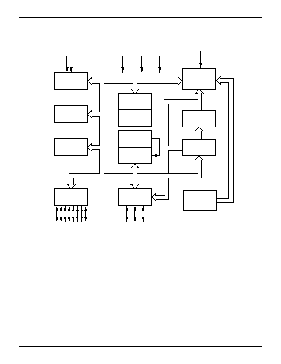
Figure 1. Z86319 Functional Block Diagram
Port 3
Counter/
Timers (2)
Interrupt
Control
Port 2
I/O
(Bit Programmable)
ALU
FLAG
Register
Pointer
Register File
144 x 8-Bit
Machine
Timing & Inst.
Control
Prg. Memory
2048 x 8-Bit
Program
Counter
GND
RCIN
VDD
Input
Port 0
I/O
AGND
WDT

Z86319
Zilog
PS/2 Mouse Controller
DS97KEY1605
P R E L I M I N A R Y
3
1
PIN DESCRIPTIONS
Figure 2. 18-Pin DIP/SOIC Pin Configuration
Table 1. 18-Pin DIP/SOIC Pin Identification
Pin #
Symbol
Function
Direction
1-4
P24-P27
Port 2, Pins 4,5,6,7
In/Output
5
V
DD
Power Supply
Power
6
RCIN
RC Oscillator
Input
7
AGND
Analog Ground
Ground
8
P31
Port 3, Pin 1
Input
9
GND
Ground
Input
10
P33
Port 3, Pin 3,
Input
11-13
P00-P02
Port 0, Pins 0,1,2
In/Output
14
GND
Ground
Ground
15-18
P20-P23
Port 2, Pins 0,1,2,3
In/Output
P24
P25
P26
P27
VDD
RCIN
AGND
P31
GND
P23
P22
P21
P20
GND
P02
P01
P00
P33
18
18 - Pin
DIP/SOIC
1
9
10

Z86319
PS/2 Mouse Controller
Zilog
4
P R E L I M I N A R Y
DS97KEY1605
PIN FUNCTIONS
RCIN.
A precision 1% resistor is connected to RCIN,
generating oscillation with an internal capacitor.
Resistor values and corresponding typical frequencies are
shown in Table 2 and graph chart (Figure 3).
Table 2. Resistor Values and Corresponding
Typical Frequencies
External Resistor
Average Frequency
14.0K
5.01 MHz
15.0K
4.70 MHz
16.0K
4.43 MHz
17.0K
4.19 MHz
18.0K
3.97 MHz
19.0K
3.78 MHz
20.0K
3.60 MHz
21.0K
3.44 MHz
22.0K
3.30 MHz
23.0K
3.16 MHz
Figure 3. Z86319 RC Frequency in Function of the External Resistance
(typical numbers)
0
1
2
3
4
5
6
1 4
1 5
1 6
1 7
1 8
1 9
2 0
2 1
2 2
2 3
RESISTOR VALUE (K OHMS)
FREQUENCY (MHz)

Z86319
Zilog
PS/2 Mouse Controller
DS97KEY1605
P R E L I M I N A R Y
5
1
STANDARD TEST CONDITIONS
The characteristics listed below apply for standard test
conditions as noted. All voltages are referenced to
Ground. Positive current flows into the referenced pin
(Figure 4).
ABSOLUTE MAXIMUM RATINGS
Stresses greater than those listed under Absolute Maxi-
mum Ratings may cause permanent damage to the device.
This rating is a stress rating only; operation of the device
at any condition above those indicated in the operational
sections of these specifications is not implied. Exposure to
absolute maximum rating conditions for extended periods
may affect device reliability.
CAPACITANCE
T
A
= GND = 0V, f = 1.0 MHz, unmeasured pins returned to Ground.
V
CC
SPECIFICATION
V
CC
= 4.5V to 5.5V
Using the precision RC oscillator feature, f = 4.0 MHz
±
10% under the following conditions:
s
V
CC
= 5.0V
±
10%
s
Temp 0 to 40
∞
C
s
Application board capacitance:
≠
2.0 pF max.
≠
0.5 pF min.
Figure 4. Test Load Diagram
From Output
Under Test
150 pF
I
Sym
Parameter
Min
Max
Units
V
DD
Supply Voltage*
≠0.3
+7
V
T
STG
Storage Temp
≠65
∞
+150
∞
C
T
A
Oper Ambient
Temp
0
∞
40
∞
C
Notes:
*Voltages on all pins with respect to Ground.
Parameter
Min
Max
Input Capacitance
0
10 pF
Output Capacitance
0
20 pF
I/O Capacitance
0
25 pF

Z86319
PS/2 Mouse Controller
Zilog
6
P R E L I M I N A R Y
DS97KEY1605
DC ELECTRICAL CHARACTERISTICS
4.5V
V
DD
5.5V
T
A
= 0
∞
C to +40
∞
C
Sym
Parameter
Min
Max
Units
Conditions
V
IH
Rising Input
Schmitt-Triggered
2.3
3.2
V
Note 1
V
IL
Falling Input
Schmitt-Triggered
1.3
2.2
V
Note 1
V
IL
Input Low Voltage CMOS Input
V
V
OH
Output High Voltage
V
DD
≠ 0.4
V
I
OH
= ≠2.0 mA;
V
DD
=4.5V
V
OL1
Output Low Voltage
0.4
V
I
OL
= +4.0 mA;
V
DD
=5.5V
V
OL2
Output Low Voltage
0.8
V
I
OL
= 10.0 mA,
3 Pin Max; V
DD
=5.5V
V
LV
V
CC
Low Voltage Protection
2.25
2.95
V
@ 4 MHz Max, Note 2
V
TP
Trip Point Voltage
(P24-P27)
1.9
2.5
V
P24-P27; V
DD
=5.5V
1.5
2.1
V
V
DD
=4.5V
I
IL
Input Leakage
≠1.0
1.0
µ
A
V
IN
= 0V, or V
CC
Note 4
I
OL
Output Leakage
≠1.0
1.0
µ
A
V
IN
= 0V, or V
CC
Note 4
I
DD
Supply Current
4.5
mA
@ 4 MHz, Note 3;
V
DD
=5.5V
I
DD1
Standby Current
2.2
mA
@ 4 MHz, Note 3;
V
DD
=5.5V
I
PU
Pull-Up Current (100K)
≠20
µ
A
V
IH
@ 1V
P00-02, P31, P33
≠95
µ
A
V
IH
@ 1V
I
PD
Pull-Down Current (100K)
+20
µ
A
V
IL
@ 3V
P00-02, P31, P33
+85
µ
A
V
IL
@ 4V
I
PU
Pull-Up Current (10K)
≠370
µ
A
V
IL
= 0V
P20, P22
≠670
µ
A
V
IL
= 0V
Notes:
1. The min. and max. values of the Schmitt-Trigger input voltages track each other over temperature, V
DD
, and
process variations.
2. The device is functional from V
DD
down to V
LV
voltage. The minimum operational V
DD
is determined by the value of the V
LV
voltage at ambient temperature. The V
LV
voltage increases as the temperature decreases.
3. All input pins are tied to GND and all output pins are floating.
Z86319
Zilog
PS/2 Mouse Controller
DS97KEY1605
P R E L I M I N A R Y
7
1
AC ELECTRICAL CHARACTERISTICS
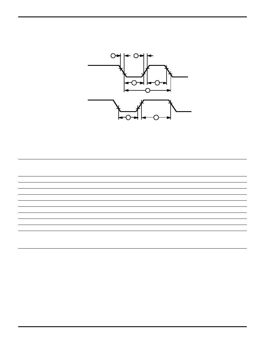
Timing Diagrams
Figure 5. Electrical Timing Diagram
2
5
T
IRQ
IN
N
4
3
1
1
6
T
A
= 0
∞
C to +40
∞
C
No
Symbol
Parameter
V
DD
Min
Max
Units
Notes
1
TrTin, TtTin
Timer Input Rise and Fall Time
5.5V
100
ns
1
2
TwTinL
Timer Input Low Width
5.5V
70
ns
1
3
TwTinH
Timer Input High Width
5.5V
2.5TpC
1
4
TpTin
Timer Input Period
5.5V
4TpC
1
5
TwIL
Int. Request Input Low Time
5.5V
70
ns
1,2
6
TwIH
Int. Request Input High Time
5.5V
2.5TpC
1,2
Twdt
Watch-Dog Timer Time Out
5.5V
10
ms
TPOR
Power-On Reset Time
5.5V
2
10
ms
TpC
RC Oscillator Clock Period
5.5V
220
5000
ns
Notes:
1. Timing Reference uses 0.9 V
DD
for a logic 1 and 0.1 V
DD
for a logic 0.
2. Interrupt request through Port 3 (P33-P31)
Z86319
PS/2 Mouse Controller
Zilog
8
P R E L I M I N A R Y
DS97KEY1605
PIN FUNCTIONS
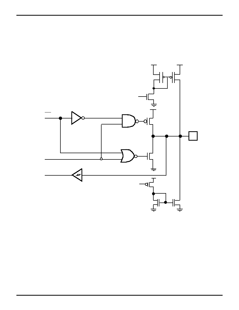
Port 0 (P02-P00). Port 0 is a 3-bit, I/O programmable, bi-
directional, CMOS-compatible I/O port. These three I/O
lines can be configured under software control to be input
or output (Figure6). When Port 0 is configured as an input
port, all lines have the capability to either sink or source
(ROM mask selectable) current emulating a 100K pull-
down or pull-up resistor. Port 00-02 can be accessed
through the P0 register (register address 00). The upper 5
bits of this 8-bit register always reads "11111." Writing to
the upper 5 bits has no effect (see Figure 34). The lower 3
bits of the P0 register are read/write. Current versus pin
voltage graphs are shown in Figures 7 and 8.
Figure 6. Port 0 Configuration
OE
Out
In
Pad
Pull-Down / Enable
(Mask Option)
Pull-Up Enable
(Mask Option)

Z86319
Zilog
PS/2 Mouse Controller
DS97KEY1605
P R E L I M I N A R Y
9
1
Figure 7. Current vs Pin Voltage Values
vdrain
Figure 8. Current vs Pin Voltage Values
Z86319
PS/2 Mouse Controller
Zilog
10
P R E L I M I N A R Y
DS97KEY1605
PIN FUNCTIONS (Continued)
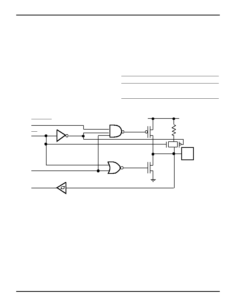
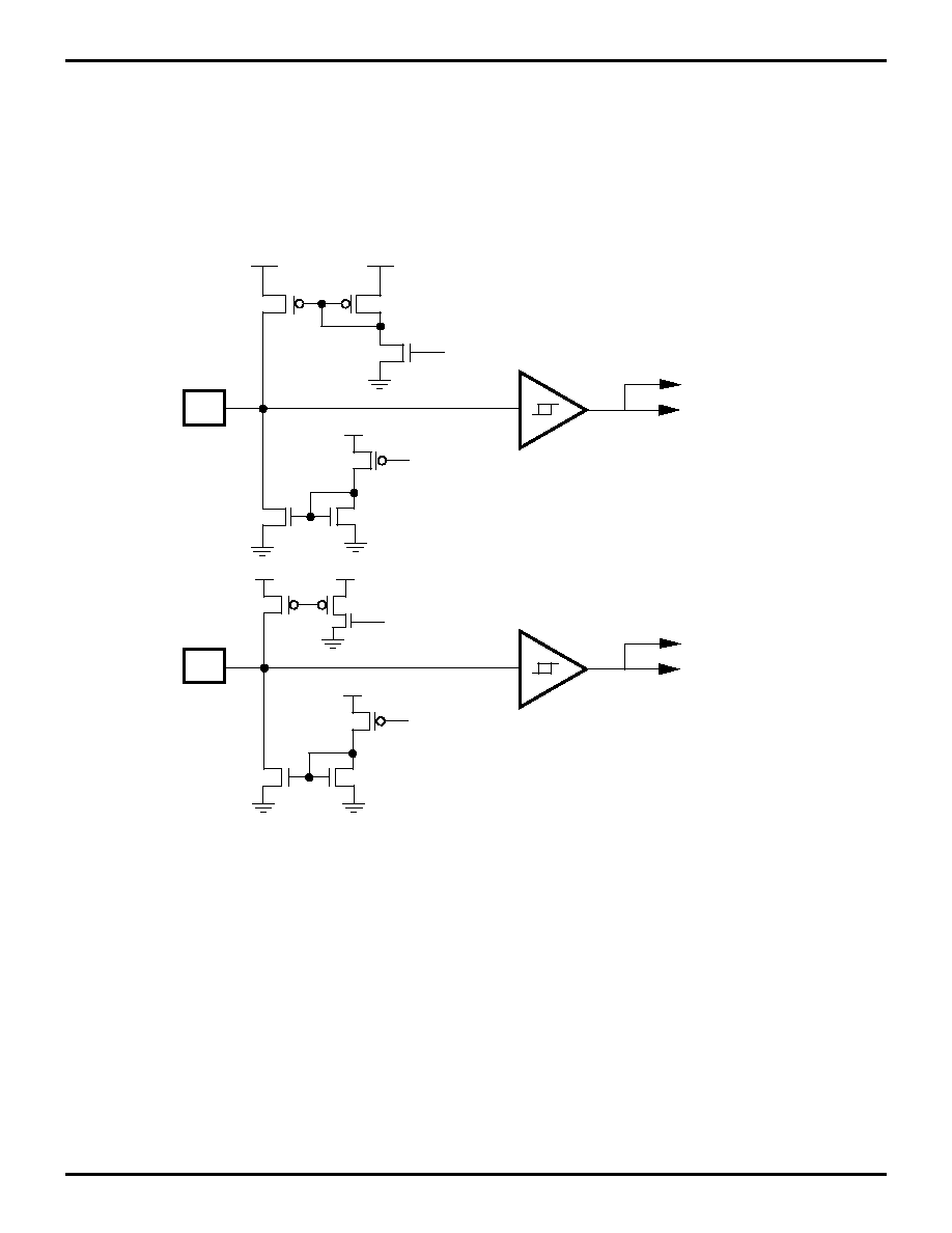
Port 2 (P27-P20). Port 2 is an 8-bit, bit programmable, bi-
directional, CMOS-compatible I/O port. These eight I/O
lines can be configured under software control to be input
or output, independently. Bits programmed as outputs
may be globally programmed as either push-pull or open-
drain. When configured as inputs, P20 and P22 have 10
kOhm (typical) pull-up resistors (Figure 9). However, P21
and P23 do not have resistors (Figure 10).
When configured as inputs, P24-P27 are configured with a
voltage divider. The voltage divider consists of an internal
25K pull-up resistor (Figure 11), and a 7.5K pull-down re-
sistor. The input levels on P24-P27 are adjusted for con-
nection to the emitters of the opto-transistors and switch at
a voltage level of 0.4 V
DD
(
±
300 mV). For input voltages
on P24-P27, refer to Table 3.
Table 3. P24-P27 Input Open Circuit Voltage
(No off-chip resistance)
V
DD
Min
Max
4.5V
0.95V
1.15V
5.0V
1.05V
1.25V
5.5V
1.15V
1.39V
Figure 9. Port 2 P20, P22 Configuration
OE
Out
In
Open-Drain
V
DD
Pad
10 Kohm,
±
20%

Z86319
Zilog
PS/2 Mouse Controller
DS97KEY1605
P R E L I M I N A R Y
11
1
Figure 10. Port 2 P21, P23 Configuration
OE
Out
In
Open-Drain
VDD
Pad
Figure 11. Port 2 P27-P24 Configuration
OE
Out
In
Pad
Open-Drain
0.4 VDD
±
300 mV
Trip Point Buffer
7.5K
25K
Resistance Tolerance (0-40
∞
C)
Min.
Max.
Pull-Down
Pull-Up
5.2K
8.9K
18K
30K
Z86319
PS/2 Mouse Controller
Zilog
12
P R E L I M I N A R Y
DS97KEY1605
PIN FUNCTIONS (Continued)
Port 3 (P33, P31). Port 3 is a 2-bit, CMOS-compatible
port with two fixed input lines (P33, P31). These two lines
can also be used as the interrupt sources IRQ2 and IRQ1.
P31 can also be configured as a timer input. Both lines can
be configured through ROM mask selection to sink or
source current emulating a 100K pull-up or pull-down re-
sistor (Figure 12). Port 33-31 can be accessed through
the P3 register. The upper 4 bits of this 8-bit register al-
ways reads "1111." Bit D2 reads 0 and Bit D0 reads 1. Bits
D3 and D1 represent P33 and P31 respectively (see Fig-
ure 36).
Figure 12. Port 3 P33, P31 Configuration
P31
Pad
P33
IRQ2, TIN
Data Latch
Data Latch
IRQ1
Pad
Pull-Up Enable
(Mask Option)
Pull-Down/Enable
(Mask Option)
Pull-Up Enable
(Mask Option)
Pull-Down/Enable
(Mask Option)

Z86319
Zilog
PS/2 Mouse Controller
DS97KEY1605
P R E L I M I N A R Y
13
1
FUNCTIONAL DESCRIPTION
The Z86319 MCU incorporates the following special fea-
tures to enhance the Z8 architectural core for use in mice,
trackballs, and other consumer applications.
Reset. Upon power-up, the Power-On Reset circuit waits
for TPOR, plus 18 clock cycles, then starts program exe-
cution at address 000CH (Figure 13). The Z86319 control
registers' reset values are shown in Table 4.
Figure 13. Internal Reset Configuration
Table 4. Z86319 Control Registers
Reset Values
Addr.
Reg.
D7
D6
D5
D4
D3
D2
D1
D0
Comments
F1
TMR
0
0
0
0
0
0
0
0
F2
T1
U
U
U
U
U
U
U
U
F3
PRE1
U
U
U
U
U
U
0
0
F4
T0
U
U
U
U
U
U
U
U
F5
PRE0
U
U
U
U
U
U
U
0
F6
P2M
1
1
1
1
1
1
1
1
Inputs after reset
F7
P3M
U
U
U
U
U
U
1
0
F8
P01M
U
U
U
0
U
U
0
1
F9
IPR
U
U
U
U
U
U
U
U
FA
IRQ
U
U
0
0
0
0
0
0
FB
IMR
0
U
U
U
U
U
U
U
FC
FLAGS
U
U
U
U
U
U
U
U
FD
RP
U
U
U
U
U
U
U
U
FF
SPL
U
U
U
U
U
U
U
U
Delay
TPOR
18 CLK
Reset Filter
Chip
Reset
RC OSC
POR
(Cold Start)

Z86319
PS/2 Mouse Controller
Zilog
14
P R E L I M I N A R Y
DS97KEY1605
FUNCTIONAL DESCRIPTION (Continued)
Program Memory. The Z86319 can address up to 2 KB
of internal program memory (Figure 14). The first 12 bytes
of program memory are reserved for the interrupt vectors.
These locations contain four 16-bit vectors that corre-
spond to the four available interrupts. Bytes 0-2047 are
on-chip mask-programmed ROM.
Register File. The Register File consists of three I/O
port registers, 125 general-purpose registers, and 14 con-
trol and status registers, R0-R3, R4-R127 and R241-
R255, respectively (Figure 15). The Z86319 instructions
can access registers directly or indirectly via an 8-bit ad-
dress field. This field allows short, 4-bit register addressing
using the Register Pointer. In the 4-bit mode, the register
file is divided into eight working register groups, each oc-
cupying 16 continuous locations. The Register Pointer ad-
dresses the starting location of the active working-register
group.
Figure 14. Program Memory Map
On-Chip
ROM
Location of
First Byte of
Instruction
Executed
After RESET
Interrupt
Vector
(Lower Byte)
Interrupt
Vector
(Upper Byte)
IRQ5
IRQ4
IRQ4
Reserved
Reserved
IRQ2
IRQ2
IRQ1
IRQ1
Reserved
Reserved
IRQ5
2047
12
11
10
9
8
7
6
5
4
3
2
1
0
Figure 15. Register File
Stack Pointer (Bits 7-0)
R255
General-Purpose
Register Pointer
Program Control Flags
Interrupt Mask Register
Interrupt Request Register
Interrupt Priority Register
Ports 0-1 Mode
Port 3 Mode
Port 2 Mode
T0 Prescaler
Timer/Counter0
T1 Prescaler
Timer/Counter1
Timer Mode
General-Purpose
Registers
Port 3
Port 2
Reserved
Port 0
R254
R253
R252
R251
R250
R249
R248
R247
R246
R245
R244
R243
R242
R241
R240
R127
R3
R2
R1
R0
SPL
RP
FLAGS
IMR
IRQ
IPR
P01M
P3M
P2M
PRE0
T0
PRE1
T1
TMR
P3
P2
P0
R4
LOCATION
IDENTIFIERS
Not Implemented
GPR
R128

Z86319
Zilog
PS/2 Mouse Controller
DS97KEY1605
P R E L I M I N A R Y
15
1
Stack Pointer. The Z86319 features an 8-bit Stack
Pointer (R255) used for the internal stack that resides with-
in the general-purpose registers.
Counter/Timer. There are two 8-bit programmable
counter/timers (T0 and T1), each driven by its own 6-bit
programmable prescaler. The T1 prescaler can be driven
by internal or external clock sources, however, the T0 can
be driven by the internal clock source only (Figure 16).
The 6-bit prescalers can divide the input frequency of the
clock source by any integer number from 1 to 64. Each
prescaler drives its counter, which decrements the value
(1 to 256) that has been loaded into the counter. When
both counter and prescaler reach the end of count, a timer
interrupt request IRQ4 (T0) or IRQ5 (T1) is generated.
The counter can be programmed to start, stop, continue,
or restart from the initial value. The counters can also be
programmed to stop upon reaching zero (single pass
mode) or to automatically reload the initial value and contin-
ue counting (modulo-n continuous mode).
The counters, but not the prescalers, are read at any time
without disturbing their value or count mode. The clock
source for T1 is user-definable and can be either the inter-
nal microprocessor clock divided by four, or an external
signal input via Port 3. The Timer Mode register configures
the external timer input (P31) as an external clock, a trigger
input that is retriggerable or not retriggerable, or as a gate
input for the internal clock.
Figure 16. Counter/Timers Block Diagram
PRE0
Initial Value
Register
T0
Initial Value
Register
T0
Current Value
Register
6-Bit
Down
Counter
8-Bit
Down
Counter
˜
4
OSC
6-Bit
Down
Counter
8-Bit
Down
Counter
PRE1
Initial Value
Register
T1
Initial Value
Register
T1
Current Value
Register
Clock
Logic
IRQ4
IRQ5
Internal Data Bus
Write
Write
Read
Internal Clock
Gated Clock
Triggered Clock
Write
Write
Read
Internal Data Bus
External Clock
Internal
Clock
˜
4
T P31
IN
Z86319
PS/2 Mouse Controller
Zilog
16
P R E L I M I N A R Y
DS97KEY1605
FUNCTIONAL DESCRIPTION (Continued)
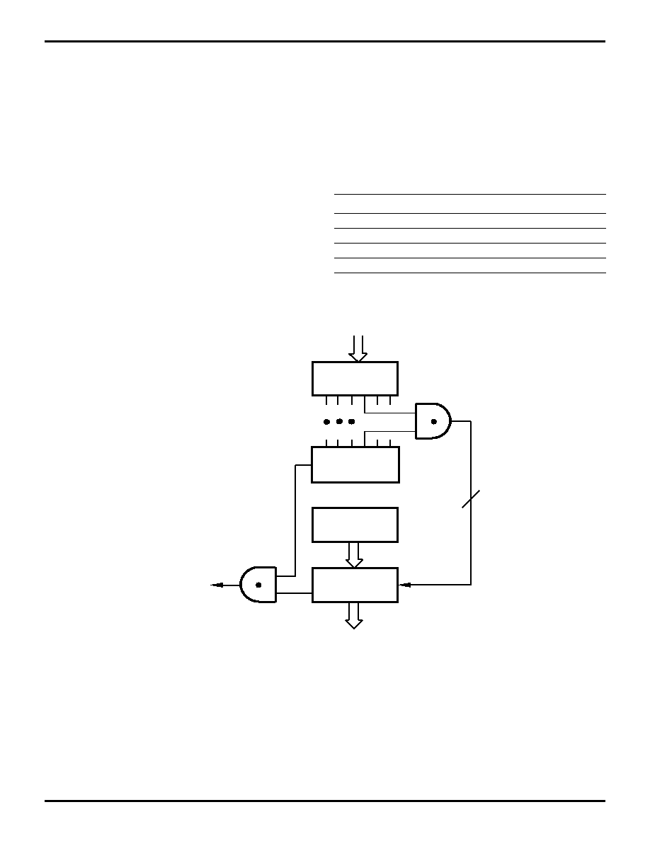
Interrupts. The Z86319 features four interrupts from
four different sources. These interrupts are maskable and
prioritized (Figure 17). The four sources are divided as fol-
lows: the falling edge of P31, P33, and the two
counter/timers. The Interrupt Mask Register globally or in-
dividually enables or disables the four interrupt requests
(Table 5).
When more than one interrupt is pending, priorities are re-
solved by a programmable priority encoder that is con-
trolled by the Interrupt Priority register. All Z86319 inter-
rupts are vectored through locations in program memory.
When an interrupt machine cycle is activated, an interrupt
request is granted, thereby disabling all subsequent inter-
rupts, saving the Program Counter and Status Flags, and
branching to the program memory vector location reserved
for that interrupt. This memory location and the next byte
contain the 16-bit starting address of the Interrupt Service
Routine for that particular interrupt request.
To accommodate polled interrupt systems, interrupt inputs
are masked and the Interrupt Request Register is polled to
determine which of the interrupt requests requires service.
Table 5. Interrupt Types, Sources, and Vectors
Source
Name
Vector
Location Comments
P33
IRQ1
2,3
External
Falling Edge
P31
IRQ2 4,5
External
Falling
Edge
T0
IRQ4
8,9
Internal
T1
IRQ5 10,11
Internal
Figure 17. Interrupt Block Diagram
IRQ
IMR
IPR
Priority
Logic
6
Vector Select
Global
Interrupt
Enable
Interrupt
Request
IRQ1 - IRQ5
Z86319
Zilog
PS/2 Mouse Controller
DS97KEY1605
P R E L I M I N A R Y
17
1
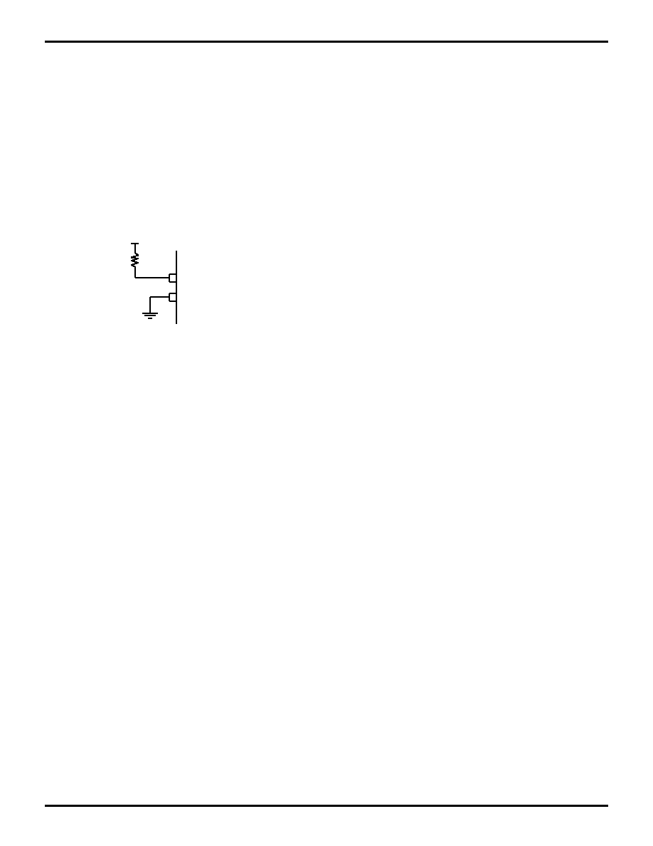
RC Oscillator. The Z86319 features an on-chip RC pre-
cision oscillator that requires a 1% precision resistor exter-
nally connected between V
DD
and pin 6 (Figure 18). The
tolerance of the RC oscillator is less than
±
10% over the
voltage range of 4.5V to 5.5V and over a temperature
range of 0-40
∞
C. Pin 7 is the Analog Ground for the oscilla-
tor.
Increased parasitic board capacitance will slow down the
RC oscillator and deteriorate the RC frequency tolerance.
The minimum and maximum parasitic board capacitances
are 0.5 pF and 2 pF, respectively.
HALT Mode. This instruction turns off the internal CPU
clock but not the precision RC oscillator. The counter/tim-
ers, their interrupts, and external interrupts IRQ1 and IRQ2
remain active. The device can be recovered by interrupts,
either externally or internally generated. An interrupt must
be enabled prior to the HALT Mode, and executed to exit
the HALT Mode. After the interrupt service routine, the
program continues from the instruction after the HALT.
In order to enter HALT Mode, it is necessary to first flush
the instruction pipeline to avoid suspending execution in
mid-instruction. To flush the pipeline, the user must exe-
cute a NOP (Opcode=FFH) immediately before the HALT
instruction. i.e.:
In HALT Mode, the value of each output line prior to the
HALT instruction is retained.
Watch-Dog Timer (WDT). The Watch-Dog Timer is en-
abled upon power-up of the MCU and is clocked by its own
internal RC oscillator. The WDT instruction does not affect
the Zero (Z), Sign (S), and Overflow (V) flags.
Opcode WDT (5FH). Execution of WDT clears the WDT
counter. The time interval between any 2 consecutive
WDT instructions has to be smaller than T
WDT
min.
Low Voltage Protection (V
LV
). The device will func-
tion normally between 5.5V and 4.5V under all specified
conditions. Below 4.5V, the device is still internally func-
tional until the Low Voltage trip point (V
LV
) is reached,
however, it is not guaranteed to meet all AC and DC Char-
acteristics. When the supply voltage drops below V
LV
, an
automatic hardware reset occurs as V
DD
returns above
V
LV
. Essentially, this action helps in reinitializing the
Z86319.
The actual V
LV
is a function of temperature, operating fre-
quency and process parameters. The typical V
LV
is a
function of the ambient temperature for a frequency of 4
MHz. The device is functional down to V
LV
voltage. The
min. operational V
DD
is determined by the value of the V
LV
voltage at ambient temperatures. The V
LV
voltage in-
creases as the temperature decreases (Figure 19).
Figure 18. Oscillator Configuration
FF
NOP
; clear the pipeline
7F
HALT
; enter the HALT Mode
VDD
1%
6
RCIN
AGND
7
Precision
RC Oscillator

Z86319
PS/2 Mouse Controller
Zilog
18
P R E L I M I N A R Y
DS97KEY1605
FUNCTIONAL DESCRIPTION (Continued)
Figure 19. Typical Z86319 VLV vs Temperature
2.80
2.75
2.70
2.65
2.60
2.55
2.50
≠5
0
5
10
15
20
25
30
35
40
Temperature (
∞
C)
2.45
2.40
2.35
V
LV
(Typical)
2.85
Volts

Z86319
Zilog
PS/2 Mouse Controller
DS97KEY1605
P R E L I M I N A R Y
19
1
Z8 CONTROL REGISTERS
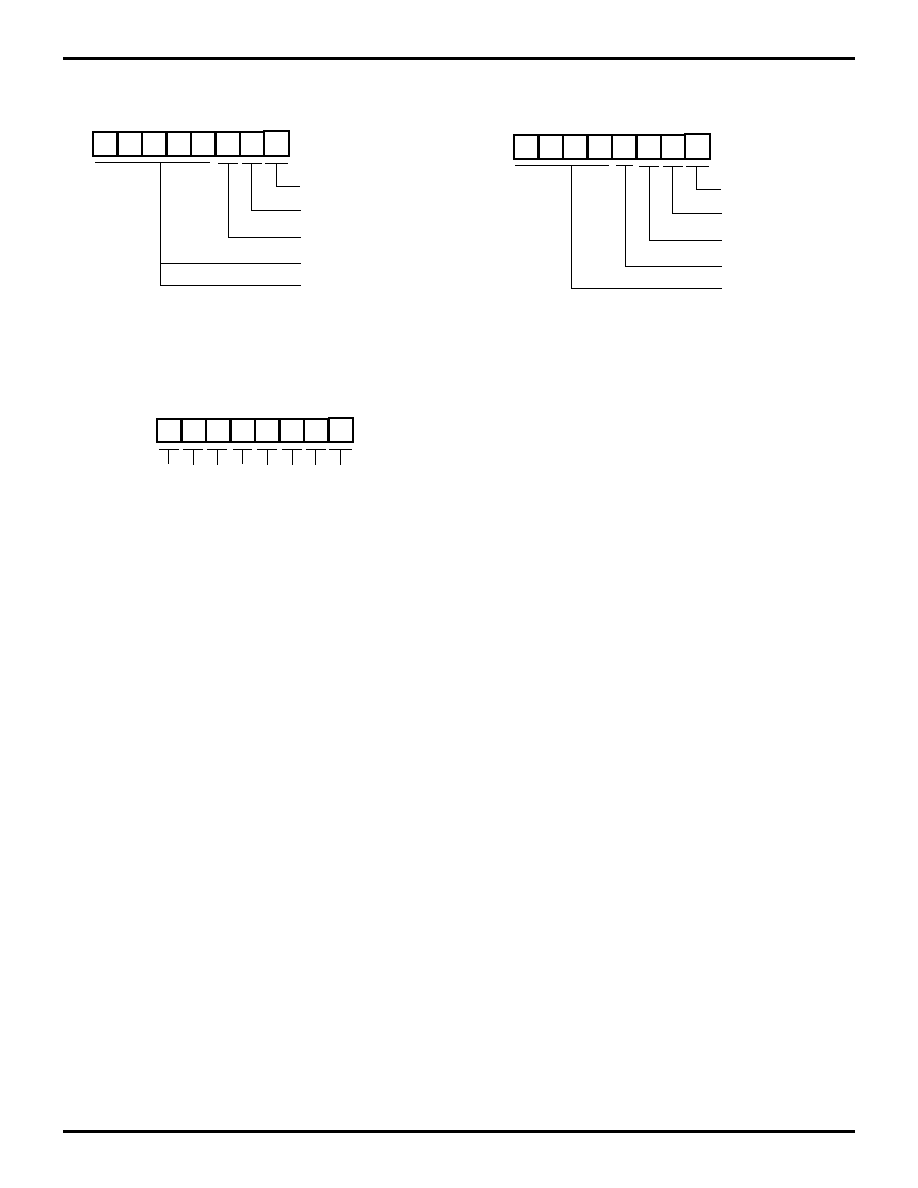
Figure 20. Timer Mode Register
(F1H: Read/Write)
Figure 21. Counter Timer 1 Register
(F2H: Read/Write)
Figure 22. Prescaler 1 Register
(F3H: Write Only)
D7 D6
D5
D4
D3 D2
D1
D0
0 Disable T0 Count
1 Enable T0 Count
0 No Function
1 Load T0
0 No Function
1 Load T1
0 Disable T1 Count
1 Enable T1 Count
TIN Modes
00 External Clock Input
01 Gate Input
10 Trigger Input
(Non-retriggerable)
11 Trigger Input
(Retriggerable)
Reserved (Must be 0)
R241 TMR
D7
D6
D5
D4
D3
D2
D1
D0
T1 Initial Value
(When Written)
(Range 1-256 Decimal
01-00 HEX)
T1 Current Value
(When READ)
R242 T1
D7
D6
D5
D4
D3
D2
D1
D0
Count Mode
0 T1 Single Pass
1 T1 Modulo
Clock Source
1 T1 Internal
0 T1 External Timing Input
(TIN) Mode
Prescaler Modulo
(Range: 1-64 Decimal
01-00 HEX)
R243 PRE1
Figure 23. Counter/Timer 0 Register
(F4H: Read/Write)
Figure 24. Prescaler 0 Register
(F5H: Write Only)
Figure 25. Port 2 Mode Register
(F6H: Write Only)
Figure 26. Port 3 Mode Register
(F7H: Write Only)
D7
D6
D5
D4
D3
D2
D1
D0
T0 Initial Value
(When Written)
(Range: 1-256 Decimal
01-00 HEX)
T0 Current Value
(When READ)
R244 T0
0 T0 Single Pass
1 T0 Modulo N
D7
D6
D5 D4
D3
D2
D1
D0
Count Mode
Reserved (Must be 0)
Prescaler Modulo
(Range: 1-64 Decimal
01-00 HEX)
R245 PRE0
D7
D6
D5
D4
D3
D2
D1
D0
P27- P20 I/O Definition
0 Defines Bit as OUTPUT
1 Defines Bit as INPUT
R246 P2M
0 Port 2 Open-Drain
1 Port 2 Push-Pull
D7 D6
D5
D4
D3 D2
D1
D0
Reserved (Must be 0)
R247 P3M

Z86319
PS/2 Mouse Controller
Zilog
20
P R E L I M I N A R Y
DS97KEY1605
Z8 CONTROL REGISTERS (Continued)
Figure 27. Port 0 and 1 Mode Register
(F8H: Write Only)
Figure 28. Interrupt Priority Register
(F9H: Write Only)
Figure 29. Interrupt Request Register
(FAH: Read/Write)
D7
D6
D5
D4
D3
D2
D1
D0
R248 P01M
P00-P03 Mode
0 Output
1 Input
Reserved (Must be 0)
Don't care
Reserved (Must be 0)
D7 D6
D5
D4
D3
D2
D1
D0
Reserved
(Must be 0.)
R249 IPR
0000
0001
0010
0011
0100
0101
0110
0111
1000
1001
1010
1011
1100
1101
1110
1111
Reserved
IRQ1>4>5>2
Reserved
IRQ4>1>5>2
IRQ5>2>1>4
IRQ5>1>4>2
IRQ5>2>4>1
IRQ5>4>1>2
IRQ2>1>4>5
IRQ1>4>2>5
IRQ2>4>1>5
IRQ4>1>2>5
IRQ2>5>1>4
Reserved
IRQ2>5>4>1
Reserved
D7 D6
D5
D4
D3 D2
D1
D0
R250 IRQ
IRQ2 = P31 Input
IRQ1 = P33 Input
IRQ4 = T0
IRQ5 = T1
Reserved (Must be 0)
Reserved (Must be 0)
Reserved (Must be 0)
Figure 30. Interrupt Mask Register
(FBH: Read/Write)
Figure 31. Flag Register
(FCH: Read/Write)
Figure 32. Register Pointer
(FDH: Read/Write)
Figure 33. Stack Pointer
(FFH: Read/Write)
D7 D6
D5
D4
D3
D2
D1
D0
1 Enables IRQ
(DX = IRQX)
Reserved (Must be 0)
1 Enable Interrupts
R251 IMR
D7
D6
D5
D4
D3
D2
D1
D0
User Flag F1
User Flag F2
Half Carry Flag
Decimal Adjust Flag
Overflow Flag
Sign Flag
Zero Flag
Carry Flag
R252 Flags
D7
D6
D5
D4
D3
D2
D1
D0
Don't Care
Register Pointer
R253 RP
D7
D6
D5
D4
D3
D2
D1
D0
Stack Pointer Lower
Byte (SP0-SP7)
R255 SPL
Z86319
Zilog
PS/2 Mouse Controller
DS97KEY1605
P R E L I M I N A R Y
21
1
Z8 PORT REGISTERS
Figure 34. Port 0 Register (Read/Write)
Figure 35. Port 2 Register (Read/Write)
D7 D6 D5 D4 D3 D2 D1 D0
P02
Reads as "11111"
R0 Port 0
P00
P01
Writing has NO
EFFECT
D7 D6 D5 D4 D3 D2 D1 D0
R0 Port 2
P27 P26 P25 P24 P23 P22 P21 P20
Figure 36. Port 3 Register (Read Only)
D7 D6 D5 D4 D3 D2 D1 D0
Reads 0
P33
R3 Port 3
Reads 1
P31
Reads 1111
Z86319
PS/2 Mouse Controller
Zilog
22
P R E L I M I N A R Y
DS97KEY1605
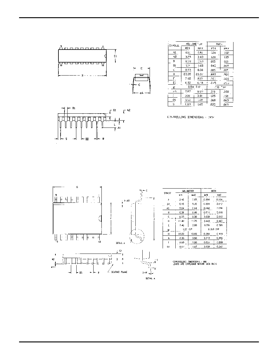
PACKAGING INFORMATION
Figure 37. 18-Pin DIP Package Diagram
Figure 38. 18-Pin SOIC Package Diagram

Z86319
Zilog
PS/2 Mouse Controller
DS97KEY1605
P R E L I M I N A R Y
23
1
ORDERING INFORMATION
For fast results, contact your local Zilog sales offices for assistance in ordering the part required.
CODES
Package
P = DIP
S = SOIC
Temperature
S = 0
∞
C to +40
∞
C
Speed
04 = 4 MHz
Environmental
C = Plastic Standard
© 1998 by Zilog, Inc. All rights reserved. No part of this
document may be copied or reproduced in any form or by
any means without the prior written consent of Zilog, Inc.
The information in this document is subject to change
without notice. Devices sold by Zilog, Inc. are covered by
warranty and patent indemnification provisions appearing
in Zilog, Inc. Terms and Conditions of Sale only.
ZILOG, INC. MAKES NO WARRANTY, EXPRESS,
STATUTORY, IMPLIED OR BY DESCRIPTION,
REGARDING THE INFORMATION SET FORTH HEREIN
OR REGARDING THE FREEDOM OF THE DESCRIBED
DEVICES FROM INTELLECTUAL PROPERTY
INFRINGEMENT. ZILOG, INC. MAKES NO WARRANTY
OF MERCHANTABILITY OR FITNESS FOR ANY
PURPOSE.
Zilog, Inc. shall not be responsible for any errors that may
appear in this document. Zilog, Inc. makes no commitment
to update or keep current the information contained in this
document.
Zilog's products are not authorized for use as critical
components in life support devices or systems unless a
specific written agreement pertaining to such intended use
is executed between the customer and Zilog prior to use.
Life support devices or systems are those which are
intended for surgical implantation into the body, or which
sustains life whose failure to perform, when properly used
in accordance with instructions for use provided in the
labeling, can be reasonably expected to result in
significant injury to the user.
Zilog, Inc. 210 East Hacienda Ave.
Campbell, CA 95008-6600
Telephone (408) 370-8000
FAX 408 370-8056
Internet: http://www.zilog.com
Z86319
Z8631904PSC
Z8631904SSC
Example:
Z 86319 0 4 P S C is a Z86319, 4 MHz, DIP, 0
∞
to +40
∞
C, Plastic Standard Flow
Environmental Flow
Temperature
Package
Speed
Product Number
Zilog Prefix