 | –≠–ª–µ–∫—Ç—Ä–æ–Ω–Ω—ã–π –∫–æ–º–ø–æ–Ω–µ–Ω—Ç: Z86C03 | –°–∫–∞—á–∞—Ç—å:  PDF PDF  ZIP ZIP |

Z86C03/C06 CMOS Z8
Æ
8-B
IT
CCP
TM
C
ONSUMER
C
ONTROLLER
P
ROCESSORS
DS95DZ80300
1
C
USTOMER
P
ROCUREMENT
S
PECIFICATION
Z86C03/C06
CMOS Z8
Æ
8-B
IT
CCP
TM
C
ONSUMER
C
ONTROLLER
P
ROCESSORS
FEATURES
Part
ROM
RAM
Speed
Z86C03
512 bytes
6 0
8 MHz
Z86C06
1 Kbyte
124
12 MHz
s
18-Pin Package (DIP, SOIC)
s
3.0 to 5.5 Volt Operating Range
s
Operating Temperature: ≠40
∞
C to +105
∞
C
s
Fast Instruction Pointer: 1.5
µ
s @ 8 MHz (C03);
1.0
µ
s @ 12 MHz (C06)
s
Multiple Expanded Register File Control Registers
and Two SPI Registers (Z86C06 only)
s
One/Two Programmable 8-Bit Counter/Timers,
Each with a 6-Bit Programmable Prescaler
s
Six Vectored, Priority Interrupts from Six Different
Sources
s
Software-Enabled Watch-Dog Timer
s
Power-On Reset Timer
s
Two Standby Modes: STOP and HALT
s
Two Comparators with Programmable Interrupt Polarity
s
14 Input/Output Lines (Two with Comparator Inputs)
s
On-Chip Oscillator that Accepts a Crystal, Ceramic
Resonator, LC, RC, or External Clock Drive.
s
Serial Peripheral Interface (SPI) (Z86C06 Only)
s
Software Programmable Low EMI Mode
s
ROM Protect Option
s
Auto Latches
GENERAL DESCRIPTION
The Z86C03/C06 CCP
TM
(Consumer Controller Proces-
sors) are members of Zilog's the Z8
Æ
single-chip micro-
controller family with enhanced wake-up circuitry, pro-
grammable watch-dog timers and low noise/EMI options.
These enhancements result in a more efficient, cost-
effective design and provide the user with increased
design flexibility over the standard Z8 microcontroller
core. With 512 and 1K bytes of ROM and 60 and 124 bytes
of general-purpose RAM, respectively, these low cost, low
power consumption CMOS microcontrollers offer fast ex-
ecution, efficient use of memory, sophisticated interrupts,
input/output bit manipulation capabilities, and easy hard-
ware/software system expansion.
The Z86C03/C06 CCP architecture is characterized by
Zilog's 8-bit microcontroller core with the addition of an
Expanded Register File to allow easy access to register
mapped peripheral and I/O circuits. The Z86C03/C06
offers a flexible I/O scheme, an efficient register and
address space structure, and a number of ancillary fea-
tures that are useful in many consumer, automotive, and
industrial applications.
For applications demanding powerful I/O capabilities, the
Z86C03/C06 provides 14 pins dedicated to input and
output. These lines are grouped into two ports and are
configurable under software control to provide timing,
status signals, or parallel I/O.
Z86C03/C06 CMOS Z8
Æ
8-B
IT
CCP
TM
C
ONSUMER
C
ONTROLLER
P
ROCESSORS
DS95DZ80300
2
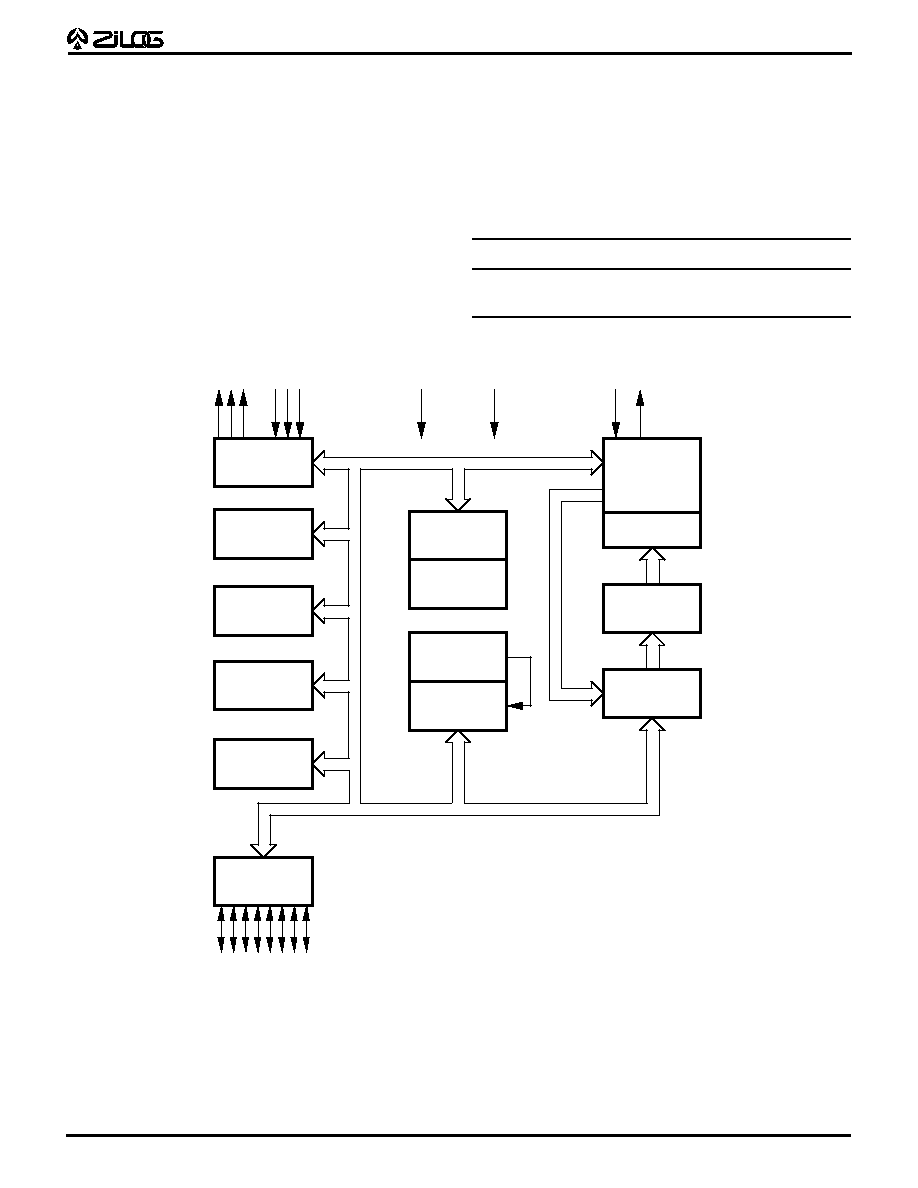
Port 3
1/2
Counter/
Timers
Interrupt
Control
Two Analog
Comparators
Port 2
I/O
(Bit Programmable)
ALU
FLAG
Register
Pointer
Register File
78/145 x 8-
Bit
Vcc
GND
XTAL
Input
Output
Machine
Timing & Inst.
Control
Prg. Memory
512/1K x 8-
Bit
Program
Counter
WDT, POR
Serial *
Peripheral
Interface
* Serial Peripheral Interface for the Z86C06 only.
Z86C03 has one counter/timer.
GENERAL DESCRIPTION
(Continued)
Three basic address spaces are available to support this
wide range of configurations: Program Memory, Register
File, and Expanded Register File. The Register File is
composed of 61/125 bytes of General-Purpose Registers,
two I/O Port registers, and 12/14 Control and Status regis-
ters. The Expanded Register File consists of three control
registers in the Z86C03, and four control registers, a SPI
Receive Buffer, and a SPI compare register in the Z86C06.
With powerful peripheral features such, as on-board com-
parators, counter/timer(s), Watch-Dog Timer (WDT), and
Serial Peripheral Interface (SPI) (C06 only), the Z86C03/
C06 meets the needs of a variety of sophisticated control-
ler applications (Figure 1).
Notes:
All Signals with a preceding front slash, "/", are active Low, e.g.:
B//W (WORD is active Low); /B/W (BYTE is active Low, only).
Power connections follow conventional descriptions below:
Connection
Circuit
Device
Power
V
CC
V
DD
Ground
GND
V
SS
Figure 1. Z86C03/C06 Functional Block Diagram

Z86C03/C06 CMOS Z8
Æ
8-B
IT
CCP
TM
C
ONSUMER
C
ONTROLLER
P
ROCESSORS
DS95DZ80300
3
1
2
9
3
4
5
6
7
8
18
17
16
15
14
13
12
11
10
P23
P22
P33
P21
P20
GND
P36
P35
P34
P24
P25
P32
P26
P27
VCC
XTAL2
XTAL1
P31
Z86C03
and
Z86C06
DIP
1
18
P24
P27
Vcc
XTAL2
XTAL1
P31
P32
P23
P22
P21
P20
GND
P36
P35
P34
P33
Z86C03
and
Z86C06
SOIC
P25
P26
2
3
4
5
6
7
8
9
17
16
15
14
13
12
11
10
PIN DESCRIPTION
Figure 2. 18-Pin DIP Pin Configuration
Table 1. 18-Pin DIP and SOIC Pin Identification
No
Symbol
Function
Direction
1-4
P24-27
Port 2, pins 4, 5, 6, 7
In/Output
5
V
CC
Power Supply
6
XTAL2
Crystal Oscillator Clock Output
7
XTAL1
Crystal Oscillator Clock Input
8-10
P31-33
Port 3, pins 1, 2, 3
Fixed Input
11-13
P34-36
Port 3, pins 4, 5, 6
Fixed Output
1 4
GND
Ground
15-18
P20-23
Port 2, pins 0, 1, 2, 3
In/Output
Figure 3. 18-Pin SOIC Pin Configuration
Z86C03/C06 CMOS Z8
Æ
8-B
IT
CCP
TM
C
ONSUMER
C
ONTROLLER
P
ROCESSORS
DS95DZ80300
4
150 pF
ABSOLUTE MAXIMUM RATINGS
Symbol
Description
Min
Max
Units
V
CC
Supply Voltage*
≠0.3
+7.0
V
V
IHM
Max Input Voltage**
1 2
V
T
STG
Storage Temp
≠65
+150
∞
C
T
A
Oper Ambient Temp
∞
C
Notes:
* Voltage on all pins with respect to GND.
** Applies to Port pins only and must limit current
going into or out of Port pins to 250
µ
A maximum.
See Ordering Information
Stresses greater than those listed under Absolute Maxi-
mum Ratings may cause permanent damage to the de-
vice. This is a stress rating only; operation of the device at
any condition above those indicated in the operational
sections of these specifications is not implied. Exposure to
absolute maximum rating conditions for extended periods
may affect device reliability.
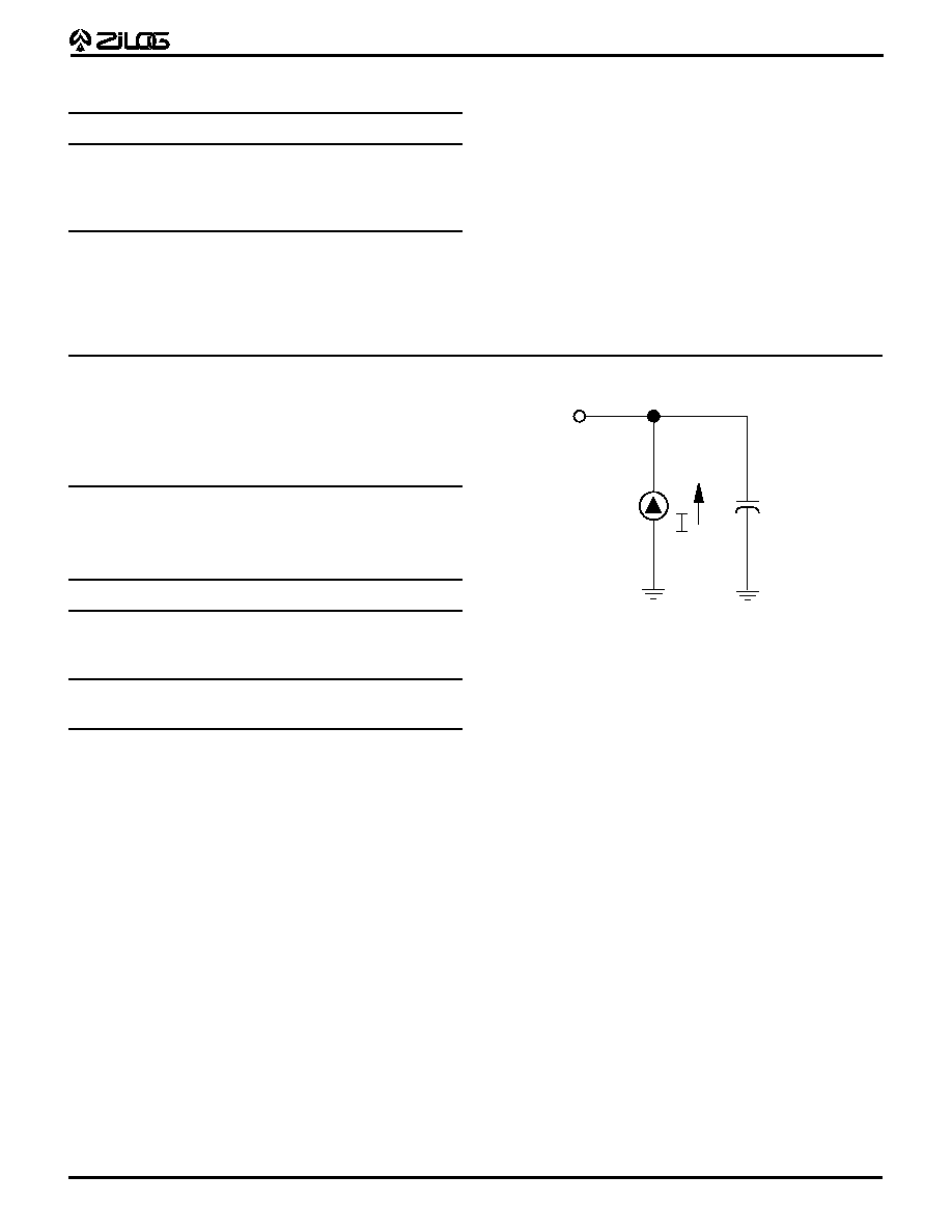
STANDARD TEST CONDITIONS
The characteristics listed below apply for standard test
conditions as noted. All voltages are referenced to Ground.
Positive current flows into the referenced pin.
Figure 4. Test Load Configuration
CAPACITANCE
T
A
= 25
∞
C, V
CC
= GND = 0V, f = 1.0 MHz, unmeasured pins
returned to GND.
Parameter
Min
Max
Input Capacitance
0
12 pF
Output Capacitance
0
20 pF
I/O Capacitance
0
25 pF
V
CC
SPECIFICATION
V
CC
= 3.0V to 5.5V

Z86C03/C06 CMOS Z8
Æ
8-B
IT
CCP
TM
C
ONSUMER
C
ONTROLLER
P
ROCESSORS
DS95DZ80300
5
DC ELECTRICAL CHARACTERISTICS
T
A
= 0
∞
C
V
CC
to +70
∞
C
Typical
Symbol Parameter
Note [3]
Min
Max
@ 25
∞
C Units
Conditions Notes
Max Input Voltage
3.3V
7
V
I
IN
250
µ
A
[7]
5.0V
7
V
I
IN
250
µ
A
[7]
V
CH
Clock Input High
3.3V
0.9 V
CC
V
CC
+0.3
2.4
V
Driven by External
Voltage
Clock Generator
5.0V
0.9 V
CC
V
CC
+0.3
3.9
V
Driven by External
Clock Generator
V
CL
Clock Input Low
3.3V
V
SS
-0.3
0.2 V
CC
1.6
V
Driven by External
Voltage
Clock Generator
5.0V
V
SS
-0.3
0.2 V
CC
2.7
V
Driven by External
Clock Generator
V
IH
Input High Voltage
3.3V
0.7 V
CC
V
CC
+0.3
1.8
V
5.0V
0.7 V
CC
V
CC
+0.3
2.8
V
V
IL
Input Low Voltage
3.3V
V
SS
-0.3
0.2 V
CC
1.0
V
5.0V
V
SS
-0.3
0.2 V
CC
1.5
V
V
OH
Output High Voltage 3.3V
V
CC
-0.4
3.1
V
I
OH
= -500
µ
A
(Low EMI Mode)
5.0V
V
CC
-0.4
4.8
V
I
OH
= -500
µ
A
V
OL
Output Low Voltage 3.3V
0.8
0.35
V
I
OL
=+1.0mA
(Low EMI Mode)
5.0V
0.4
0.18
V
I
OL
=+1.0mA
V
OH1
Output High Voltage 3.3V
V
CC
-0.4
3.1
V
I
OH
= -2.0 mA
[12]
5.0V
V
CC
-0.4
4.8
V
I
OH
= -2.0 mA
[12]
V
OL1
Output Low Voltage 3.3V
0.8
0.2
V
I
OL
= +4.0 mA
[12]
5.0V
0.4
0.1
V
I
OL
= +4.0 mA
[12]
V
OL2
Output Low Voltage 3.3V
1.0
0.4
V
I
OL
= 6 mA,
[12]
3 Pin Max
5.0V
1.0
0.5
V
I
OL
= +12 mA,
[12]
3 Pin Max
V
OFFSET
Comparator Input
3.3V
25
10
mV
Offset Voltage
5.0V
25
10
mV
I
IL
Input Leakage
3.3V
-1.0
1.0
µ
A
V
IN
= OV, V
CC
[8]
(Input bias current
5.0V
-1.0
1.0
µ
A
V
IN
= OV, V
CC
[8]
of comparator)
I
OL
Output Leakage
3.3V
-1.0
1.0
µ
A
V
IN
= OV, V
CC
5.0V
-1.0
1.0
µ
A
V
IN
= OV, V
CC
I
CC
Supply Current
3.3V
6
3.0
mA
@ 8 MHz
[4,5] [9]
5.0V
11.0
6.0
mA
@ 8 MHz
[4,5] [9]
3.3V
8.0
4.5
mA
@ 12 MHz
[4,5] [9]
5.0V
15
9.0
mA
@ 12 MHz
[4,5] [9]
Z86C03/C06 CMOS Z8
Æ
8-B
IT
CCP
TM
C
ONSUMER
C
ONTROLLER
P
ROCESSORS
DS95DZ80300
6
DC ELECTRICAL CHARACTERISTICS
(Continued)
T
A
= 0
∞
C T
A
= ≠40
∞
C
V
CC
to +70
∞
C to +105
∞
C Typical
Symbol Parameter
Note [3]
Min
Max
Min
Max
@ 25
∞
C Units
Conditions
Notes
I
CC1
Standby Current
3.3V
3.0
3.0
0.7
mA
HALT Mode V
IN
= OV, [4, 5] [10]
V
CC
@ 8 MHz
5.0V
5
5
1.5
mA
HALT Mode V
IN
= OV, [4, 5] [10] [1]
V
CC
@ 8 MHz
3.3V
4.5
4.5
1.0
mA
HALT Mode V
IN
= OV, [4, 5] [10]
V
CC
@ 12 MHz
5.0V
7.0
7.0
2.0
mA
HALT Mode V
IN
= OV, [4, 5] [10]
V
CC
@ 12 MHz
3.3V
1.4
1.4
0.6
mA
Clock Divide by 16
[4, 5] [10]
@ 8 MHz
5.0V
3.5
3.5
1.3
mA
Clock Divide by 16
[4, 5] [10]
@ 8 MHz
3.3V
2.0
2.0
0.7
mA
Clock Divide by 16
[4, 5] [10]
@ 12 MHz
5.0V
4.5
4.5
1.5
mA
Clock Divide by 16
[4, 5] [10]
@ 12 MHz
I
CC2
Standby Current
3.3V
10
20
1.0
µ
A
STOP Mode V
IN
= OV, [6] [10]
V
CC
WDT is not Running
5.0V
10
20
3.0
µ
A
STOP Mode V
IN
= OV, [6] [10]
V
CC
WDT is not Running
3.3V
350
360
180
µ
A
STOP Mode V
IN
= OV, [6] [9]
V
CC
WDT is Running
5.0V
865
875
400
µ
A
STOP Mode V
IN
= OV, [6] [9]
V
CC
WDT is Running
I
ALL
Auto Latch Low
3.3V
7.0
14.0
4.0
µ
A
OV < V
IN
< V
CC
Current
5.0V
20.0
30.0
13
µ
A
OV < V
IN
< V
CC
I
ALH
Auto Latch High
3.3V
-4.0
≠8.0
-3
µ
A
OV < V
IN
< V
CC
Current
5.0V
-9.0
≠16.0
-7
µ
A
OV < V
IN
< V
CC
T
POR
Power On Reset
3.3V
7
24
6
25
13
ms
5.0V
3
13
2
14
6.5
ms
V
BO
V
CC
Brown Out
1.50
2.65
1.2
2.95
2.4
V
2 MHz max Int. CLK Freq. [13]
Voltage
V
ICR
Comparator Input
V
CC
-1.5
V
CC
-1.5
V
Common Mode
Voltage Range
Notes:
[1]
I
CC1
Typ
Max
Unit
Freq
Clock Driven
0.3
5.0
mA
8 MHz
Crystal or Ceramic Resonator
3.0
5.0
mA
8 MHz
[2] V
SS
= 0V = GND
[3] 5.0V
±
0.5V, 3.0V
±
0.3V.
[4] All outputs unloaded, I/O pins floating, inputs at rail.
[5] C
L1
= C
L2
= 47 pF
[6] Same as note [4] except inputs at V
CC
.
[7] The input current must be limited to a maximum of 250
µ
A or less.
[8] Input bias current for comparitor inputs P31, P32, P33.
[9] Internal on-board RC is driving WDT.
[10] WDT is not running.
[11] System clock is external XTAL frequency divided by 2.
[12] Standard mode (not Low EMI Mode).
[13] The V
BO
voltage increases as the temperature decreases.

Z86C03/C06 CMOS Z8
Æ
8-B
IT
CCP
TM
C
ONSUMER
C
ONTROLLER
P
ROCESSORS
DS95DZ80300
7
Clock
1
3
4
8
2
2
3
T
IRQ
IN
N
6
5
7
7
11
Clock
Setup
10
9
Source
AC ELECTRICAL CHARACTERISTICS
Figure 5. Additional Timing
AC ELECTRICAL CHARACTERISTICS
No Symbol
Parameter
V
CC
T
A
= 0
∞
C To +70
∞
C
T
A
= -40
∞
C To +105
∞
C
Units Notes
Note[3] 8 MHz
12 MHz
8 MHz
12 MHz
Min
Max
Min
Max
Min
Max
Min
Max
1
TpC
Input Clock Period
3.3V
125
DC
83
DC
125
DC
83
DC
ns
[1]
5.0V
125
DC
83
DC
125
DC
83
DC
ns
[1]
2
TrC,TfC
Clock Input Rise
3.3V
25
15
25
15
ns
[1]
and Fall Times
5.0V
25
15
25
15
ns
[1]
3
TwC
Input Clock Width
3.3V
37
26
37
26
ns
[1]
5.0V
37
26
37
26
ns
[1]
4
TwTinL
Timer Input Low Width
3.3V
100
100
100
100
ns
[1]
5.0V
70
70
70
70
ns
[1]
5
TwTinH
Timer Input High Width 3.3V
5TpC
5TpC
5TpC
5TpC
[1] [7]
5.0V
5TpC
5TpC
5TpC
5TpC
[1] [7]
Z86C03/C06 CMOS Z8
Æ
8-B
IT
CCP
TM
C
ONSUMER
C
ONTROLLER
P
ROCESSORS
DS95DZ80300
8
AC ELECTRICAL CHARACTERISTICS
(Continued)
No Symbol
Parameter
V
CC
T
A
= 0
∞
C To +70
∞
C
T
A
= -40
∞
C To +105
∞
C
Units
Notes
Note[3]
8 MHz
12 MHz
8 MHz
12 MHz
Min
Max
Min
Max
Min
Max
Min
Max
6
TpTin
Timer Input Period
3.3V
8TpC
8TpC
8TpC
8TpC
[1] [7]
5.0V
8TpC
8TpC
8TpC
8TpC
[1] [7]
7
TrTin,
Timer Input Rise
3.3V
100
100
100
100
ns
[1]
TtTin
and Fall Timer
5.0V
100
100
100
100
ns
[1]
8
TwIL
Int. Request Input
3.3V
100
100
100
100
ns
[1,2]
Low Time
5.0V
70
70
70
70
ns
[1,2]
9
TwIH
Int. Request Input
3.3V
5TpC
5TpC
5TpC
5TpC
[1,2] [7]
High Time
5.0V
5TpC
5TpC
5TpC
5TpC
[1,2] [7]
10
Twsm
STOP Mode Recovery
3.3V
12
12
12
12
ns
Width Spec
5.0V
12
12
12
12
ns
11
Tost
Oscillator Startup Time
3.3V
5TpC
5TpC
5TpC
5TpC
Reg.
[4]
5.0V
5TpC
5TpC
5TpC
5TpC
ns
12
Twdt
Watchdog Timer
3.3V
15
15
12
12
[5]
Refresh Time
5.0V
5
5
3
3
ms
D0 = 0 [6]
D1 = 0 [6]
3.3V
30
30
25
25
ms
D0 = 1 [6]
5.0V
16
16
12
12
ms
D1 = 0 [6]
3.3V
60
60
50
50
ms
D0 = 0 [6]
5.0V
30
30
25
25
ms
D1 = 1 [6]
3.3V
250
250
200
200
ms
D0 = 1 [6]
5.0V
120
120
100
100
ms
D1 = 1 [6]
Notes:
[1] Timing Reference uses 0.9 V
CC
for a logic 1 and 0.1 V
CC
for a logic 0.
[2] Interrupt request via Port 3 (P31-P33)
[3] 5.0V
±
0.5V, 3.3V
±
0.3V
[4] SMR-D5 = 0 (Stop mode delay off)
[5] Reg. WDTMR
[6] Internal RC Oscillator only.
[7] System clock is XTAL frequency divided by 2.

Z86C03/C06 CMOS Z8
Æ
8-B
IT
CCP
TM
C
ONSUMER
C
ONTROLLER
P
ROCESSORS
DS95DZ80300
9
© 1996 by Zilog, Inc. All rights reserved. No part of this document
may be copied or reproduced in any form or by any means
without the prior written consent of Zilog, Inc. The information in
this document is subject to change without notice. Devices sold
by Zilog, Inc. are covered by warranty and patent indemnification
provisions appearing in Zilog, Inc. Terms and Conditions of Sale
only. Zilog, Inc. makes no warranty, express, statutory, implied or
by description, regarding the information set forth herein or
regarding the freedom of the described devices from intellectual
property infringement. Zilog, Inc. makes no warranty of mer-
chantability or fitness for any purpose. Zilog, Inc. shall not be
responsible for any errors that may appear in this document.
Zilog, Inc. makes no commitment to update or keep curent the
information contained in this document.
Zilog's products are not authorized for use as critical compo-
nents in life support devices or systems unless a specific written
agreement pertaining to such intended use is executed between
the customer and Zilog prior to use. Life support devices or
systems are those which are intended for surgical implantation
into the body, or which sustains life whose failure to perform,
when properly used in accordance with instructions for use
provided in the labeling, can be reasonably expected to result in
significant injury to the user.
Zilog, Inc. 210 East Hacienda Ave.
Campbell, CA 95008-6600
Telephone (408) 370-8000
FAX 408 370-8056
Internet: http://www.zilog.com