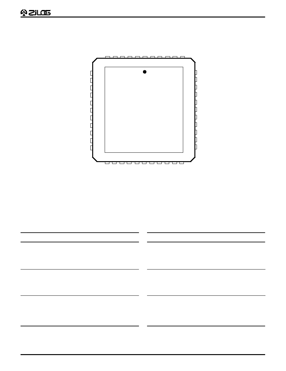
1
Z86C15
CP96KEY0603
FEATURES
ROM
RAM*
I/O
Speed
Pin Count /
(Kbytes)
(Bytes)
Lines
(MHz)
Package
4
236
3 2
5
40 DIP
44 PLCC
44 QFP
* General-Purpose
n
4.5- to 5.5-Volt Operating Range
n
0
�
C to 70
�
C Operating Temperature Range
n
Expanded Register File
n
Low-Power Consumption: 30 mW @ 5 MHz Typical
n
Six Vectored, Priority Interrupts from
Six Different Sources
n
Two Programmable 8-Bit Counter/Timers,
Each with 6-Bit Programmable Prescaler
n
Power-On Reset (POR) Timer, Hardware Watch-Dog
Timer (WDT)
n
Digital Inputs CMOS Levels with
Internal Pull-Up Resistors
n
Four Direct Connect LED Drive Ports
n
On-Chip RC Oscillator, 4 MHz to 5 MHz
GENERAL DESCRIPTION
The Z86C15 Keyboard Controller is a full-featured mem-
ber of the Z8
�
microcontroller family offering a unique
register-to-register architecture that avoids accumulator
bottlenecks and is more code efficient than RISC
processors.
For applications demanding powerful I/O capabilities, the
Z86C15 provides 32 pins dedicated to input and output.
These lines are grouped into four ports, each port consist-
ing of eight lines, and are configurable under software
control to provide timing, status signals, and serial or
parallel I/O ports.
Two on-chip counter/timers, with a large number of user-
selectable modes, are available to relieve the system of
administering real-time tasks, such as counting/timing and
I/O datacommunications.
Six different internal or external interrupt sources are
maskable and prioritized so a vectored address is pro-
vided for efficient interrupt subroutine handling and
multitasking functions.
CP96KEY0603 (3/96)
C
USTOMER
P
ROCUREMENT
S
PECIFICATION
The Z86C15 achieves low-EMI by means of several modi-
fications in the output drivers and clock circuitry of the
device.
By means of an expanded register file, the designer has
access to three additional system control registers that
provide extra peripheral devices, I/O ports, and register
addresses (see Functional Block Diagram).
Notes:
All Signals with a preceding front slash, "/", are active Low, e.g.,
B//W (WORD is active Low); /B/W (BYTE is active Low, only).
Power connections follow conventional descriptions below:
Connection
Circuit
Device
Power
V
CC
V
DD
Ground
GND
V
SS
Z86C15
CMOS Z8
�
8-B
IT
MCU
K
EYBOARD
C
ONTROLLER

2
Z86C15
CP96KEY0603
GENERAL DESCRIPTION
(Continued)
Z86C15 Functional Block Diagram
Port 3
Counter/
Timers (2)
Interrupt
Control
Port 2
I/O
(Bit Programmable)
ALU
Flags
Register
Pointer
Register File
258 x 8-Bit
Machine
Timing & Inst.
Control
Program
Memory
Program
Counter
Vcc
GND
RCIN
CLKOUT
/RESET
Output
Input
Port 0
Port 1
I/O
(Nibble Programmable)
I/O
(Byte Programmable)
4
4
8
WDT
POR
/WDT
OUT

3
Z86C15
CP96KEY0603
40-Pin DIP Pin Configuration
40-Pin DIP Pin Identification
Pin #
Symbol
Function
Direction
1
V
CC
Power Supply
Input
2
CLKOUT
Z8 System Clock
Output
3
RCIN
RC Oscillator Clock
Input
4
P37
Port 3, Pin 7
Output
5
P30
Port 3, Pin 0
Input
6
/RESET
Reset
Input
7
AGND
Analog Ground
*8
NC
Not Connected
9
/WDTOUT
Watch-Dog Timer
Output
1 0
P35
Port 3, Pin 5
Output
Pin #
Symbol
Function
Direction
1 1
GND
Ground
1 2
P32
Port 3, Pin 2
Input
13-20 P00-P07
Port 0, Pins 0,1,2,3,4,5,6,7 In/Output
21-28 P10-P17
Port 1, Pins 0,1,2,3,4,5,6,7 In/Output
2 9
P34
Port 3, Pin 4
Output
3 0
P33
Port 3, Pin 3
Input
31-38 P20-P27
Port 2, Pins 0,1,2,3,4,5,6,7 In/Output
3 9
P31
Port 3, Pin 1
Input
4 0
P36
Port 3, Pin 6
Output
PIN IDENTIFICATION
1
2
3
4
5
6
7
8
9
10
11
12
13
14
15
16
17
18
19
20
VCC
CLKOUT
RCIN
P37
P30
/RESET
AGND
*NC
/WDTOUT
P35
GND
P32
P00
P01
P02
P03
P04
P05
P06
P07
P36
P31
P27
P26
P25
P24
P23
P22
P21
P20
P33
P34
P17
P16
P15
P14
P13
P12
P11
P10
40
39
38
37
36
35
34
33
32
31
30
29
28
27
26
25
24
23
22
21
Z86C15
DIP
*Note: Pin 8 is connected to the chip, although it is
used only for testing. This pin must float.

4
Z86C15
CP96KEY0603
PIN IDENTIFICATION
(Continued)
44-Pin PLCC Pin Assignments
Pin #
Symbol
Function
Direction
14-16
P00-P02
Port 0, Pins 0, 1, 2
In/Output
1 7
N/C
Not Connected
18-22
P03-P07
Port 0, Pins 3, 4, 5, 6, 7
In/Output
23-27
P10-P14
Port 1, Pins 0, 1, 2, 3, 4
In/Output
2 8
N/C
Not Connected
29-31
P15-P17
Port 1, Pins 5, 6, 7
In/Output
3 2
P34
Port 3, Pin 4
Output
3 3
P33
Port 3, Pin 3
Input
34-38
P20-P24
Port 2, Pins 0, 1, 2, 3, 4
In/Output
3 9
N/C
Not Connected
40-42
P25-P27
Port 2, Pins 5, 6, 7
In/Output
4 3
P31
Port 3, Pin 1
Input
4 4
P36
Port 3, Pin 6
Output
Pin #
Symbol
Function
Direction
1
V
CC
Power Supply
Input
2
CLKOUT
Z8 System Clock
Output
3
RCIN
RC Oscillator Clock
Input
4
P37
Port 3, Pin 7
Output
5
P30
Port 3, Pin 0
Input
6
N/C
Not Connected
7
/RESET
Reset
Input
8
AGND
Analog Ground
*9
N/C
Not Connected
1 0
/WDTOUT Watch-Dog Timer
Output
1 1
P35
Port 3, Pin 5
Output
1 2
GND
Ground
1 3
P32
Port 3, Pin 2
Input
44-Pin PLCC Pin Identification
N/C
P30
P37
RCIN
CLKOUT
VCC
P36
P31
P27
P26
P25
P03
P04
P05
P06
P07
P10
P1
1
P12
P13
P14
N/C
N/C
P24
P23
P22
P21
P20
P33
P34
P17
P16
P15
/RESET
AGND
*N/C
/WDTOUT
P35
GND
P32
P00
P01
P02
N/C
7
8
9
10
11
12
13
14
15
16
17
38
37
36
35
34
33
32
31
30
29
39
Z86C15
PLCC
6
5
4
3
2
1
44 43 42 41 40
18 19 20 21 22 23 24 25 26 27 28
*Note: Pin 9 is connected to the chip, although it is used
only for testing. This pin must float.

5
Z86C15
CP96KEY0603
44-Pin QFP Pin Assignments
Pin # Symbol
Function
Direction
1
/RESET
Reset
Input
2
AGND
Analog Ground
*3
N/C
Not Connected
4
/WDTOUT Watch-Dog Timer
Output
5
P35
Port 3, Pin 5
Output
6
GND
Ground
7
P32
Port 3, Pin 2
Input
8-10
P00-P02
Port 0, Pins 0, 1, 2
In/Output
1 1
N/C
Not Connected
Input
12-16 P03-P07
Port 0, Pins 3,4,5,6,7
In/Output
17-21 P10-P14
Port 1, Pins 0,1,2,3,4
In/Output
2 2
N/C
Not Connected
23-25 P15-P17
Port 1, Pins 5, 6,7
In/Output
44-Pin QFP Pin Identification
Pin # Symbol
Function
Direction
2 6
P34
Port 3, Pin 4
Output
2 7
P33
Port 3, Pin 3
Input
28-32 P20-P24
Port 2, Pins 0, 1, 2, 3, 4
In/Output
3 3
N/C
Not Connected
34-36 P25-P27
Port 2, Pins 5, 6, 7
In/Output
3 7
P31
Port 3, Pin 1
Input
3 8
P36
Port 36
Output
3 9
V
CC
Power Supply
4 0
CLKOUT
Z8 System Clock
Output
4 1
RCIN
RC Oscillator Clock
Input
4 2
P37
Port 3, Pin 7
Output
4 3
P30
Port 3, Pin 0
Input
4 4
N/C
Not Connected
1
2
3
4
5
6
7
8
9
10
11
Z86C15
QFP
44 43 42 41 40 39 38 37 36 35 34
12
/RESET
AGND
*N/C
/WDTOUT
P35
GND
P32
P00
P01
P02
N/C
13 14 15 16 17 18 19 20 21 22
33
32
31
30
29
28
27
26
25
24
23
N/C
P24
P23
P22
P21
P20
P33
P34
P17
P16
P15
N/C
P30
P37
RCIN
CLKOUT
VCC
P36
P31
P27
P26
P25
P03
P04
P05
P06
P07
P10
P1
1
P12
P13
P14
N/C
*Note: Pin 3 is connected to the chip, although it is used
only for testing. This pin must float.


