
1
Z86C21 MCU
WITH
8K ROM
P
RODUCT
S
PECIFICA
TION
s
8-Bit CMOS MCU with 8 Kbytes of ROM
s
256 Byte Register File
- 236 Bytes of General-Purpose RAM
- 16 Bytes Control/Status Registers
- 4 Bytes for Ports
s
40-Pin DIP, 44-Pin PLCC or 44-Pin QFP Package
s
4.5V to 5.5V Operating Range
s
Low Power Consumption: 220 mW (max) @ 16 MHz
s
Fast instruction pointer: 1.0
µ
s @ 12 MHz
s
Two Standby Modes: STOP and HALT
s
32 Input/Output Lines
FEATURES
Z86C21
8K ROM Z8
Æ
CMOS
M
ICROCONTROLLER
s
Full-Duplex UART
s
All Digital Inputs are TTL Levels
s
Auto Latches
s
RAM and ROM Protect
s
Two Programmable 8-Bit Counter/Timers each with
6-Bit Programmable Prescaler.
s
Six Vectored, Priority Interrupts from Eight Different
Sources
s
Clock Speeds: 12 and 16 MHz
s
On-Chip Oscillator that Accepts a Crystal, Ceramic
Resonator, LC, or External Clock Drive.
GENERAL DESCRIPTION
The Z86C21 microcontroller is a member of the Z8 single-
chip microcontroller family with 8 Kbytes of ROM and
236 bytes of RAM. The device is packaged in a 40-pin DIP,
44-pin PLCC, or a 44-pin QFP with a ROMless pin option
available on the 44-pin versions only. With the ROM/
ROMless feature selectively, the Z86C21 offers both exter-
nal memory and preprogrammed ROM, making it well-
suited for high-volume applications or where code flexibil-
ity is required.
Zilog's CMOS microcontroller offers fast execution, effi-
cient use of memory, sophisticated interrupts, input/output
bit manipulation capabilities, and easy hardware/software
system expansion along with low cost and low power
consumption.
The Z86C21 architecture is characterized by Zilog's 8-bit
microcontroller core. The device offers a flexible I/O
scheme, an efficient register and address space structure,
multiplexed capabilities between address/data, I/O, and a
number of ancillary features that are useful in many indus-
trial and advanced scientific applications.
For applications demanding powerful I/O capabilities, the
Z86C21 provides 32 pins dedicated to input and output.
These lines are grouped into four ports. Each port consists
of eight lines, and is configurable under software control to
provide timing, status signals, serial or parallel
I/O with or without handshake, and an address/data bus
for interfacing external memory. There are three basic
address spaces available to support this configuration:
Program Memory, Data Memory, and 236 general-pur-
pose registers.
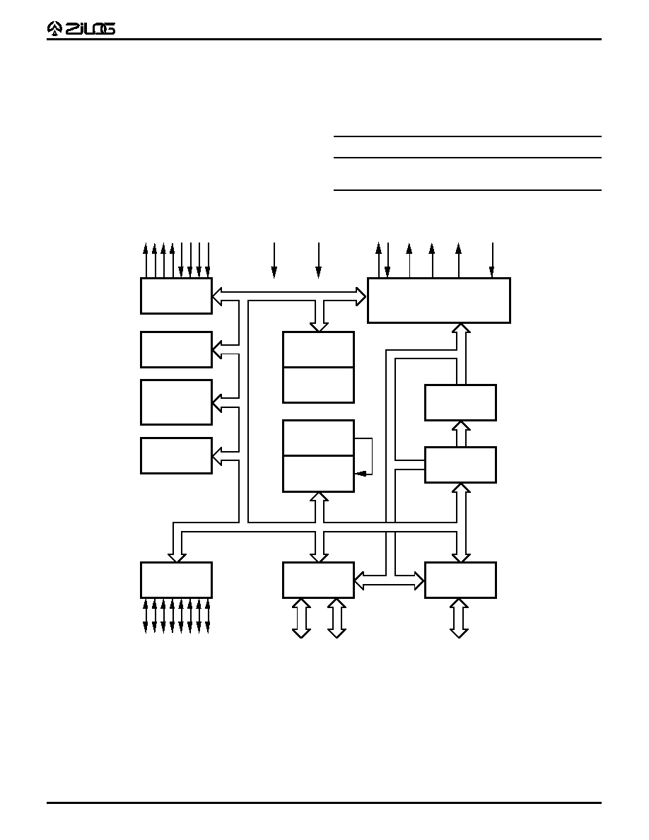
\2
Z86C21 MCU
WITH
8K ROM
GENERAL DESCRIPTION
(Continued)
To unburden the program from coping with the real-time
tasks, such as counting/timing and serial data communi-
cation, the Z86C21 offers two on-chip counter/timers with
a large number of user selectable modes, and an on-board
UART.
Port 3
UART
Counter/
Timers
(2)
Interrupt
Control
Port 2
I/O
(Bit Programmable)
ALU
FLAGS
Register
Pointer
Register File
256 x 8-Bit
Machine Timing and
Instruction Control
Prg. Memory
8192 x 8-Bit
Program
Counter
Vcc
GND
XTAL
4
4
Port 0
Output
Input
Address or I/O
(Nibble Programmable)
8
Port 1
Address/Data or I/O
(Byte Programmable)
/AS /DS R//W /RESET
Figure 1. Z86C21 Functional Block Diagram
Notes:
All Signals with a preceding front slash, "/", are active Low, e.g.,
B//W (WORD is active Low); /B/W (BYTE is active Low, only).
Power connections follow conventional descriptions below:
Connection
Circuit
Device
Power
V
CC
V
DD
Ground
GND
V
SS
3
Z86C21 MCU
WITH
8K ROM
PIN DESCRIPTION
Pin #
Symbol
Function
Direction
1
V
CC
Power Supply
Input
2
XTAL2
Crystal, Oscillator Clock
Output
3
XTAL1
Crystal, Oscillator Clock
Input
4
P37
Port 3, Pin 7
Output
5
P30
Port 3, Pin 0
Input
6
/RESET
Reset
Input
7
R//W
Read/Write
Output
8
/DS
Data Strobe
Output
9
/AS
Address Strobe
Output
10
P35
Port 3, Pin 5
Output
Pin #
Symbol
Function
Direction
11
GND
Ground
Input
12
P32
Port 3, Pin 2
Input
13-20
P00-P07
Port 0, Pins 0,1,2,3,4,5,6,7 In/Output
21-28
P10-P17
Port 1, Pins 0,1,2,3,4,5,6,7 In/Output
29
P34
Port 3, Pin 4
Output
30
P33
Port 3, Pin 3
Input
31-38
P20-P27
Port 2, Pins 0,1,2,3,4,5,6,7 In/Output
39
P31
Port 3, Pin 1
Input
40
P36
Port 3, Pin 6
Output
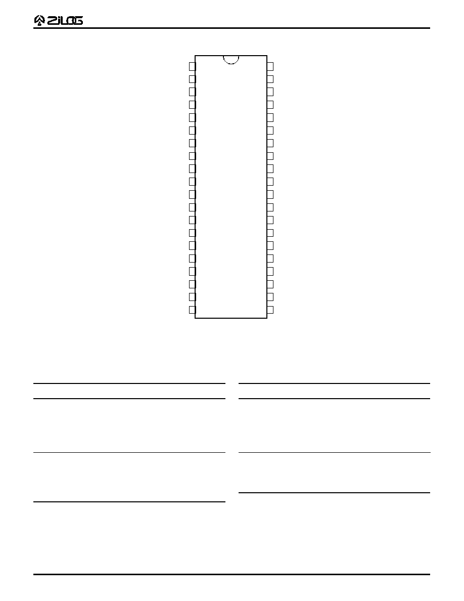
Table 1. 40-Pin DIP Pin Identification
1
2
9
3
4
5
6
7
8
40
39
38
37
36
35
34
33
32
P36
P31
P21
P27
P26
P25
P24
P23
P22
VCC
XTAL2
P37
P30
/RESET
R//W
/DS
31
30
29
28
27
14
10
11
12
13
XTAL1
GND
P32
P00
P01
P20
P33
P34
P17
P16
Z86C21
DIP
15
26
25
24
23
22
21
20
16
17
18
19
/AS
P35
P02
P03
P06
P07
P05
P04
P13
P15
P14
P12
P11
P10
Figure 2. 40-Pin DIP Pin Assignments
\4
Z86C21 MCU
WITH
8K ROM
PIN DESCRIPTION
(Continued)
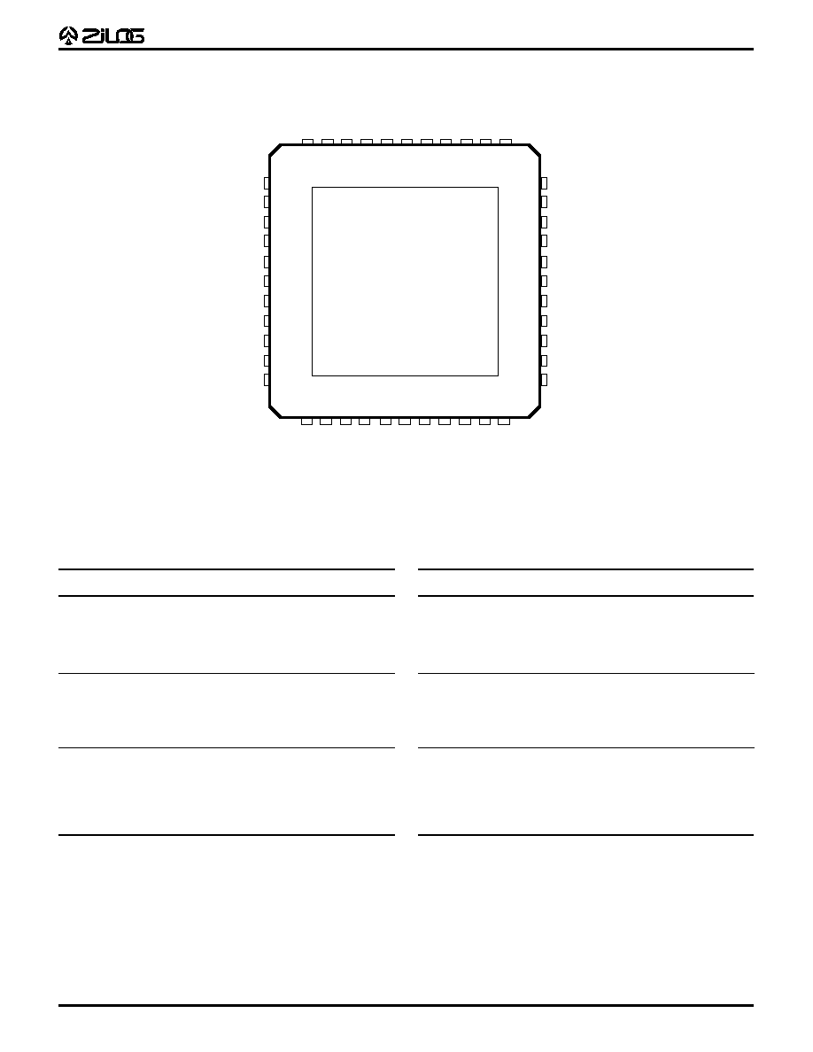
N/C
P30
P37
XTAL1
XTAL2
VCC
P36
P31
P27
P26
P25
P03
P04
P05
P06
P07
P10
P11
P12
P13
P14
N/C
N/C
P24
P23
P22
P21
P20
P33
P34
P17
P16
P15
/RESET
R//W
/DS
/AS
P35
GND
P32
P00
P01
P02
R//RL
7
8
9
10
11
12
13
14
15
16
17
38
37
36
35
34
33
32
31
30
29
39
Z86C21
PLCC
6
5
4
3
2
1
44 43 42 41 40
18 19 20 21 22 23 24 25 26 27 28
Table 2. 44-Pin PLCC Pin Identification
Pin #
Symbol
Function
Direction
14-16
P00-P02
Port 0, Pins 0,1,2
In/Output
17
R//RL
ROM/ROMless control
Input
18-22
P03-P07
Port 0, Pins 3,4,5,6,7
In/Output
23-27
P10-P14
Port 1, Pins 0,1,2,3,4
In/Output
28
N/C
Not Connected
Input
29-31
P15-P17
Port 1, Pins 5,6,7
In/Output
32
P34
Port 3, Pin 4
Output
33
P33
Port 3, Pin 3
Input
34-38
P20-P24
Port 2, Pins 0,1,2,3,4
In/Output
39
N/C
Not Connected
Input
40-42
P25-P27
Port 2, Pins 5,6,7
In/Output
43
P31
Port 3, Pin 1
Input
44
P36
Port 3, Pin 6
Output
Pin #
Symbol
Function
Direction
1
V
CC
Power Supply
Input
2
XTAL2
Crystal, Oscillator Clock
Output
3
XTAL1
Crystal, Oscillator Clock
Input
4
P37
Port 3, Pin 7
Output
5
P30
Port 3, Pin 0
Input
6
N/C
Not Connected
Input
7
/RESET
Reset
Input
8
R//W
Read/Write
Output
9
/DS
Data Strobe
Output
10
/AS
Address Strobe
Output
11
P35
Port 3, Pin 5
Output
12
GND
Ground
Input
13
P32
Port 3, Pin 2
Input
Figure 3. 44-Pin PLCC Pin Assignments
5
Z86C21 MCU
WITH
8K ROM
34
35
36
37
38
39
40
41
42
43
44
21
20
19
18
17
16
15
14
13
12
22
33 32 31 30 29 28 27 26 25 24 23
1
2
3
4
5
6
7
8
9
10
11
GND
P30
P37
XTAL1
XTAL2
VCC
P36
P31
P27
P26
P25
/RESET
R//W
/DS
/AS
P35
GND
P32
P00
P01
P02
R//RL
GND
P24
P23
P22
P21
P20
P33
P34
P17
P16
P15
P03
P04
P05
P06
P07
P10
P11
P12
P13
P14
GND
Z86C21
QFP
Table 3. 44-Pin QFP Pin Identification
Pin #
Symbol
Function
Direction
1-5
P03-P07
Port 0, Pins 3,4,5,6,7
In/Output
6
GND
Ground
Input
7-14
P10-P17
Port 1, Pins 0 through 7
In/Output
15
P34
Port 3, Pin 4
Output
16
P33
Port 3, Pin 3
Input
17-21
P20-P24
Port 2, Pins 0,1,2,3,4
In/Output
22
GND
Ground
Input
23-25
P25-P27
Port 2, Pins 5,6,7
In/Output
26
P31
Port 3, Pin 1
Input
27
P36
Port 3, Pin 6
Output
28
GND
Ground
Input
29
V
CC
Power Supply
Input
30
XTAL2
Crystal, Oscillator Clock
Output
Pin #
Symbol
Function
Direction
31
XTAL1
Crystal, Oscillator Clock
Input
32
P37
Port 3, Pin 7
Output
33
P30
Port 3, Pin 0
Input
34
/RESET
Reset
Input
35
R//W
Read/Write
Output
36
/DS
Data Strobe
Output
37
/AS
Address Strobe
Output
38
P35
Port 3, Pin 5
Output
39
GND
Ground
Input
40
P32
Port 3, Pin 2
Input
41-43
P00-P02
Port 0, Pins 0,1,2
In/Output
44
R//RL
ROM/ROMless control
Input
Figure 4. 44-Pin QFP Pin Assignments